KR850000278B1 - Synchronous detector - Google Patents
Synchronous detector Download PDFInfo
- Publication number
- KR850000278B1 KR850000278B1 KR1019800003707A KR800003707A KR850000278B1 KR 850000278 B1 KR850000278 B1 KR 850000278B1 KR 1019800003707 A KR1019800003707 A KR 1019800003707A KR 800003707 A KR800003707 A KR 800003707A KR 850000278 B1 KR850000278 B1 KR 850000278B1
- Authority
- KR
- South Korea
- Prior art keywords
- carrier
- signal
- register
- vector
- phase
- Prior art date
- Legal status (The legal status is an assumption and is not a legal conclusion. Google has not performed a legal analysis and makes no representation as to the accuracy of the status listed.)
- Expired
Links
Images







Classifications
-
- H—ELECTRICITY
- H04—ELECTRIC COMMUNICATION TECHNIQUE
- H04L—TRANSMISSION OF DIGITAL INFORMATION, e.g. TELEGRAPHIC COMMUNICATION
- H04L27/00—Modulated-carrier systems
- H04L27/18—Phase-modulated carrier systems, i.e. using phase-shift keying
- H04L27/22—Demodulator circuits; Receiver circuits
-
- H—ELECTRICITY
- H04—ELECTRIC COMMUNICATION TECHNIQUE
- H04L—TRANSMISSION OF DIGITAL INFORMATION, e.g. TELEGRAPHIC COMMUNICATION
- H04L27/00—Modulated-carrier systems
- H04L27/18—Phase-modulated carrier systems, i.e. using phase-shift keying
- H04L27/22—Demodulator circuits; Receiver circuits
- H04L27/233—Demodulator circuits; Receiver circuits using non-coherent demodulation
- H04L27/2335—Demodulator circuits; Receiver circuits using non-coherent demodulation using temporal properties of the received signal
- H04L27/2337—Demodulator circuits; Receiver circuits using non-coherent demodulation using temporal properties of the received signal using digital techniques to measure the time between zero-crossings
-
- H—ELECTRICITY
- H03—ELECTRONIC CIRCUITRY
- H03D—DEMODULATION OR TRANSFERENCE OF MODULATION FROM ONE CARRIER TO ANOTHER
- H03D3/00—Demodulation of angle-, frequency- or phase- modulated oscillations
-
- H—ELECTRICITY
- H04—ELECTRIC COMMUNICATION TECHNIQUE
- H04L—TRANSMISSION OF DIGITAL INFORMATION, e.g. TELEGRAPHIC COMMUNICATION
- H04L7/00—Arrangements for synchronising receiver with transmitter
- H04L7/02—Speed or phase control by the received code signals, the signals containing no special synchronisation information
- H04L7/033—Speed or phase control by the received code signals, the signals containing no special synchronisation information using the transitions of the received signal to control the phase of the synchronising-signal-generating means, e.g. using a phase-locked loop
- H04L7/0331—Speed or phase control by the received code signals, the signals containing no special synchronisation information using the transitions of the received signal to control the phase of the synchronising-signal-generating means, e.g. using a phase-locked loop with a digital phase-locked loop [PLL] processing binary samples, e.g. add/subtract logic for correction of receiver clock
-
- H—ELECTRICITY
- H04—ELECTRIC COMMUNICATION TECHNIQUE
- H04L—TRANSMISSION OF DIGITAL INFORMATION, e.g. TELEGRAPHIC COMMUNICATION
- H04L7/00—Arrangements for synchronising receiver with transmitter
- H04L7/04—Speed or phase control by synchronisation signals
- H04L7/041—Speed or phase control by synchronisation signals using special codes as synchronising signal
- H04L7/046—Speed or phase control by synchronisation signals using special codes as synchronising signal using a dotting sequence
Landscapes
- Engineering & Computer Science (AREA)
- Computer Networks & Wireless Communication (AREA)
- Signal Processing (AREA)
- Power Engineering (AREA)
- Digital Transmission Methods That Use Modulated Carrier Waves (AREA)
- Cable Transmission Systems, Equalization Of Radio And Reduction Of Echo (AREA)
- Near-Field Transmission Systems (AREA)
Abstract
내용 없음.No content.
Description
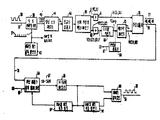
제1도는 본 발명의 동기 검파기를 구비한 통신단국의 블룩도 .1 is a block diagram of a communication end station equipped with a synchronous detector of the present invention.
제2도는 제1도에 도시된 동기검파기의 상세한 기능 블룩도.2 is a detailed functional block diagram of a synchronous detector shown in FIG.
제3도는 2진 베이스 베드 데이터 신호 및 제1도 및 제2도에 도시된 동기 검파기에 의해 수신되어 최초에 처리되는 반송파 중에 제공되는 샘플링 특성을 나타낸 그래프 A,B 및 C를 도시한 도면.FIG. 3 shows graphs A, B, and C showing the binary base bed data signal and the sampling characteristics provided during the first processed carrier received by the sync detectors shown in FIGS. 1 and 2;
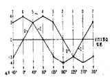
제4도는 제1도 및 제2도에 도시된 동기 검파기의 동작에 따라서 반송파 입력으로부터 도출된 샘플신호를 기억하고 또한 그 결과 얻어지는 위상 코드화된 2진 영상신호를 생성하는 방식을 예시한 그래프.4 is a graph illustrating a method of storing a sample signal derived from a carrier input and generating a resultant phase coded binary image signal according to the operation of the synchronous detector shown in FIGS. 1 and 2;
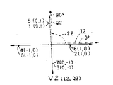
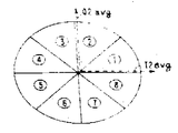
제5a도 및 제5b도는 제2도에 도시된 동기검파기에 기억된 기본 주파수 상대 위상각 벡터들 및 대응하는 1/4 삼성분들의 그래프.5A and 5B are graphs of fundamental frequency relative phase angle vectors stored in the synchronous detector shown in FIG.
제6a도 및 제6b도는 제2도에 도시된 동기검파기에 기억된 제2고조파 상대 위상각 백터들 및 대응하는 1/4 삼성분들의 그래프.6A and 6B are graphs of second harmonic relative phase angle vectors stored in the sync detector shown in FIG.
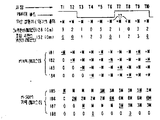
제7도는 제5b도 및 제6b도 중의 8개의 상대 위상각 기준 선과 상호 일치된 샘플계수치들에 관한 8개의 다른 위상 코드화된 2진 영상신호의 논리상태를 도시한 그래프.FIG. 7 is a graph showing the logic states of eight different phase coded binary image signals with respect to the sample coefficient values mutually matched with the eight relative phase angle reference lines in FIGS. 5B and 6B.
제8도는 제2도에 도시된 동기검파기의 동작에 응하여 생성된 기준액터 VR 및 그의 1/4 상성분들의 백터 평면을 도시한 그래프.FIG. 8 is a graph showing a vector plane of the reference actor VR and its quarter phase components generated in response to the operation of the synchronous detector shown in FIG.
제9a도, 제9b도 및 제9c도는 제2도에 다시된 동기검파기의 상세한 블룩도.9a, 9b and 9c are detailed block diagrams of the synchronous detector again in FIG.
제10도는 데이터 비트동기 동작 모드동안 제9c도의 M기억 레지스터 및 M-SUM 기억 레지스터의 동작을 에시하기 위한 시간 그래프.10 is a time graph for illustrating the operation of the M memory register and the M-SUM storage register of FIG. 9c during the data bit synchronous operation mode.
제11(a)및 제11b도는 제각기 V2avge벡터의 성분 I2avg및 Q2avg 및 VR 벡터의 성분 I R및 Q R 의 평면을 도시한 그래프로서, 제2도 및 제9b도에도시된 벡터각제산기의 동작에 따라서 제11a도 평면 중의 벡터를 2로 나누어 제11b도 평면 중의 백터를 생성하는 것을 설명하기 위한 그래프.11 (a) and 11b are graphs showing the planes of the components I2avg and Q2avg and VR vector of components IR2 and QR of the V2avge vector, respectively, according to the operation of the vector angle dividers shown in FIGS. A graph for explaining how to create a vector in the plane of FIG. 11B by dividing the vector in the plane of FIG.
제12도는 제2도와 제9a도, 제9b도 및 제9c도의 블룩도에 따라서 작동되는 동기검파기를 구비하는 시스템의 양호한 일실시예를 도시한 블룩도.FIG. 12 is a block diagram of a preferred embodiment of a system having a synchronous detector operated according to the block diagrams of FIGS. 2, 9a, 9b, and 9c.
본 발명은 2진 위상변조될 반송파를 수선하는 복수개의 통신 단국에서 사용하기 위한 개량된 동기검파기에 관한 것으로, 특히, 반송파의 서볼 떻이터 심볼 세그먼트(subdata symbol segment)를 샘플링하는 것에 의해서 도출되는 위상 코드화된 신호에 응동하여 기본주파수 및 2배 주파수의 위상각벡터 신호들을 발생하는 동기 검파기에 관한 것이다. 각각의 반송과 세그먼트를 나타내는 기본백터 신호들은 다수의 세그멘트를 나타내는 2배 주파수의 벡터 신호들로부터 도출되는 기준 기본위상각 벡터신호들과 비교되어서, 각각의 데이터 심볼에 대해 가산되는 복수개의 상관 신호들이 발생되게끔한다.The present invention relates to an improved synchronous detector for use in a plurality of communication terminals that repair a carrier to be binary phase modulated, and in particular, a phase derived by sampling a subdata symbol segment of a carrier. A synchronization detector for generating phase angle vector signals of a fundamental frequency and a double frequency in response to a coded signal. The fundamental vector signals representing each carrier and segment are compared with reference fundamental phase angle vector signals derived from vector signals of twice frequency representing multiple segments, so that a plurality of correlation signals added for each data symbol are added. Cause it to occur.
일반적으로, 반송통신 방식에 있어서, 반송파는 2진 코드화된 데이터 신호들에 의해 변조되어 전송되는데 변조된 반송파는 이후의 수선시에 반송과 신호가 감쇄, 잡음 및 기타 간섭현상, 또한 심한 산호감쇠를 초래하는 왜곡을 받게된 후에도 데이터 비트 정보가 신속하고도 신뢰성 있음은 물론 정확하게 재생되게금 검파되어야만 한다. 자동 베전형의 전력선 통신방식에 있어서, 반송과 신호는 전력선 배전도체를 통해 송전되는 전력과 더불어 전송되기 때문에 심한 간섭 임펄스 및 광대역 잡음 상태를 특히 갖게 된다. 도한 전력선 통신 시스템이 하나 이상의 송신국, 임의의 신호 중계기들 및 전력 소비요망 위치에 위치되는 극히 다수의 원격단국을 구비하고, 메시지가 코드화된 반송파 신호들은 종종 다수의 원격단국 그룹에서 동시에 수신되거나, 개개의 중계기, 또는, 단국에서 수신되게 교번 어드레싱 모드로 전송되는데, 복수주파수의 반송파 신호가 이용되는 경우, 주파수를 판별하여 신호의 상호간섭을 회피한다는 것은 실제적으로 복잡하며, 단일 주파수의 음성신호 또는 반송과 신호를 이용하는 경우, 복수의 단국 또는 중계기의 제각기에 대한 선택적인 어드레싱을 위해 다수의 메시지가 신간 다중화되기 때문에 수신단국 또는 중계기기 반송파 신호를 신속히 검출하는 것이 중요하다. 동기검파기에 파이롯트 동기신호, 즉, 비변조 동기신호를 이용하거나, 또는 코드화되고 조합된 데이터 및 동기 펄스를 이용하면 전력선 통신장치의 복잡성은 한층 중대된다. 반송파의 동기를 위해서는, 예로서, 50Hz. 또는 60Hz. 의 전력신호를 이용하는 것이 바람직하다고 알려져 있는데, 예로서 다상선로들간의 위상천이로 인해 전력선로에 나타나는 불연속성 때문에, 상기한 바와 같은 전력신호는 이용될수 있을지는 몰라도 항상 신뢰성 있는 외부 동기수단으로서의 역할을 행해지는 못한다.In general, in a carrier communication scheme, a carrier is modulated and transmitted by binary coded data signals, and the modulated carrier may cause attenuation of carriers and signals in subsequent repairs, noise and other interferences, and severe coral attenuation. Even after receiving the resulting distortion, the data bit information must be detected to be reproduced quickly and reliably and accurately. In the automatic power line communication system, the carrier and the signal are transmitted along with the power transmitted through the power line distribution conductor, and thus have particularly severe interference impulse and broadband noise conditions. In addition, the powerline communication system has one or more transmitting stations, arbitrary signal repeaters and an extremely large number of remote stations located at the power consumption location, and the message coded carrier signals are often received simultaneously in multiple groups of remote stations, It is transmitted in the alternating addressing mode to be received by individual repeaters or stations, and when a multi-frequency carrier signal is used, it is practically complicated to discriminate frequencies and avoid mutual interference of signals. When using carriers and signals, it is important to quickly detect the receiving station or repeater carrier signal since multiple messages are newly multiplexed for selective addressing of each of a plurality of stations or repeaters. The complexity of the power line communication device is further increased by using a pilot synchronization signal, i. For synchronization of the carrier, for example, 50 Hz. Or 60 Hz. It is known that it is preferable to use a power signal of. For example, due to the discontinuity in the power line due to the phase shift between the polyphase lines, the power signal as described above may always be used as a reliable external synchronization means. Can't be done.
주파수편이 피변조 반송파 신호에 대해 종종 사용되는 바와 같은 비동기 검파기에 있어서, 반송과 신호의 진폭 포탁선은 종종 메시지의 개시를 호가실하게 알 수 있게 하는데 사용된다. 잡음 임펄스 및 스파이크는 종종 메시지의 오개시 통지원으로 작용하여 수신기에서 좋지 못한 어드레스 해독동작 및 기타의 에매모호만 동작을 야기하여 성능의 저하를 초래한다. 따라서, 전력선 반송통신 방식의 수신단국에 대한 일반적인 검파요건들은 잡음 및 기타의 간섭신호가 존재하는 경우에 반송신호를 최적하에 검파하는 것과, 반송파 신호의 존재여부를 검출하기 위한 근거를 선택하는 것과, 수신기 및 검파기 동작의 이상적인 성능으로 부터의 편차가 거의 없게 하는 것과, 수신기 및 검파기를 반송파 신호에 동기시키는 것과, 코드화된 메시지정보의 각각의 데이터비트와 동기하는 것과, 최초에 전송된 바와 같은 메시지 정보의 데이데 비트들을 최후에 무오차 재생하게금 데이터 비트의 2진 상태와 극성동기하는 것을 포함하는데, 이들 요건을 양보하게 만족하기 위해서, 위상 변조된 복수의 반송파 신호, 즉, 위상 편이 피변조형 또는 동기 위상 피변조형의 반송파 신호는 반송파 위상관계로 포함된 반송 데이터를 재생하는 데 이용되어서, 반송파의 포락선 진폭을 관측할 피료요가 없게끔 한다. 수신된 위상 피변조 반송파신호의 신호처리 조정방법은 광대역에서 잡음 스파이크를 제한하고 클리핑한 후 협대역에서 증폭하고 신호 제한하여, 동기검파기의 입력측에서 재생용 반송파가 광대역의 잡음 임펄스에 덜 민감하게끔 하는 것이다.In an asynchronous detector as is often used for frequency shifted carrier signals, the carrier and amplitude envelope of the signal are often used to make the beginning of the message obscure. Noise impulses and spikes often act as notification sources for misdiagnosis of messages, resulting in poor address resolution and other emphatic operations at the receiver, leading to performance degradation. Accordingly, general detection requirements for a receiving end station of a power line carrier communication method include optimally detecting a carrier signal in the presence of noise and other interference signals, selecting a basis for detecting the presence of a carrier signal, Little deviation from the ideal performance of receiver and detector operation, synchronizing the receiver and detector to carrier signals, synchronizing with each data bit of coded message information, and message information as originally transmitted Polarization synchronization with the binary state of the data bits for the last error free reproduction of the data bits of the data bits, in order to yield these requirements, a plurality of phase modulated carrier signals, i. E. The carrier signal of the synchronous phase modulated type reproduces the carrier data contained in the carrier phase relationship. It is to be used, and not gekkeum piryo yoga to observe the envelope amplitude of the carrier. The signal processing adjustment method of the received phase-modulated carrier signal limits noise spikes in the wideband, clipping, amplifies in the narrowband, and limits the signal so that the reproduction carrier at the input side of the synchronous detector is less sensitive to the wideband noise impulse. will be.
종종 등기 위상 변조신호의 검파에 있어서는 국부적으로 발생되거나 발진하는 신호가 상관관계의 개시전에 도태신호에 동기될 필요가 있다. 수신된 데이터를 검파하기 위한 신호처리전에는 어떤 실제의 시간이 필요하다.Often in the detection of registered phase modulated signals, locally generated or oscillated signals need to be synchronized to the select signal prior to the start of correlation. Some actual time is required before signal processing to detect the received data.
다른 일반적인 위상 검출기술은 소위 차동위상 편이 피변조형 기술을 들 수 있는데, 이 기술에서는 도 래신호가 지연선로에 인가되고, 직전의 데이터 비트와의 비교를 위해 처리되어서 선행하는 데이터 비트와 동일한 극성 도ㅓ는 역극성의 신호가 출력되게 한다. 이같은 형태의 위상 검출기술에 있어서의 결점은 기준기술이 단일의 비트만에 포함된 정보를 사용하며, 처리중의 데이터 비트에 포함되는 것과 동일한 정도의 많은 잡음을 포함하여 성능의 저하를 가져온다는 것이다. 차동위상편이 변조방식은 간혹 저데이러율로 작동되어 한층 정확한 무오차의 작동을 보증하지만, 이에 의하면 소정의 기간중에 전송될 수 있는 데이터량이 제한된다.Another common phase detection technique is a so-called differential phase shift modulated technique, in which the incoming signal is applied to a delay line and processed for comparison with the immediately preceding data bit so that it has the same polarity as the preceding data bit. 되게 causes the signal of reverse polarity to be output. The drawback with this type of phase detection technique is that the reference technique uses information contained in only a single bit and results in performance degradation, including as much noise as is contained in the data bits being processed. . Differential phase shift modulation is sometimes operated at low data rates to ensure more accurate error free operation, but this limits the amount of data that can be transmitted during a given period of time.
따라서, 본 발명의 목적은 독특하게 조합되고 제어되는 최소의 동작을 이용하여, 전력선 통신 방식의 수신용 통신 단국에서의 이용에 특히 적합한 시스템이 제공 되게금 최적한 성능은 물론이거니와 간단하고도 신뢰성 있는 동작을 행하는 동기 검파기를 제공하는데 있다.It is therefore an object of the present invention to provide a system which is particularly suited for use in a receiving communication station of power line communication mode, using a uniquely combined and controlled minimum operation, so as to provide optimum performance as well as simple and reliable operation. To provide a synchronous detector that performs
상기한 목적의 판점에서 본 발명은 전력선 반송통신방식에 이용하는데 특히 적합한 2진 위상 편이 피변조 반송파로부터 도출된 복수의 방형과 펄스신호를 변조하는 데이터 비트 신호에 대한 동기 검파기에 있어서, 상기 방형과 펄스신호를 샘플링하고 방형과 펄스신호의 제1레벨 및 제2레벨에 상당하는 두개의 2진 논리상태중의 어는 것을 갖는 복수의 극성 샘플 비트를 생성하되, 상기 샘플비트로 이루어진 소정의 동등한 복수 그룹이 각각의 데이터 비트기간 중에 주기적으로 생기도록 하기 위한 장치와, 소정의 동등한 복수그룹이 응동하여, 각각의 그룹에 대해 기본 주파수에서의 상대 위상각 표시를 갖는 복수의 제1벡터 성분 신호를 갖는 복수의 기준 벡터 성분신호를 발생하기 위한 장치와, 상기 소정의 동등한 복수 그룹에 응동하여 상기 기본 주파수에서의 상대 위상각 표시를 갖는 복수의 기준 벡터 성분신호를 발생하기 위한 장치와, 상기 복수의 제1 벡터 성분 신호들과 상기 복수의 기준 벡터 성분 신호들의 각각의 위상비교에 응동하여 복수의 상관신호를 발생하기 위한 위상검출기와, 복수의 동등한 데이터 비트기간 중에 생기는 상기 소정의 동등한 복수 그룹의 각각으로부터 발생된 상기 복수의 제1벡터 성분 신호들의 위상 비교에 응동하여 상기 복수의 상관신호를 선택적으로 가산하는 위상 검출기 출력합계 회로를 구비한 것을 특징으로 하는 동기 검파기에 있다.In view of the above object, the present invention provides a synchronization detector for a data bit signal that modulates a plurality of squares and pulse signals derived from a binary phase shift modulated carrier, which is particularly suitable for use in power line carrier communication. Sampling a pulse signal and generating a plurality of polar sample bits having any of two binary logic states corresponding to the square and the first level and the second level of the pulse signal; A device for generating periodically during each data bit period, and a plurality of predetermined equivalent groups of pluralities having a plurality of first vector component signals having relative phase angle indications at the fundamental frequency for each group. An apparatus for generating a reference vector component signal and the basic principal in response to the predetermined equal plurality of groups; A device for generating a plurality of reference vector component signals having a relative phase angle representation in a number, and a plurality of correlations in response to respective phase comparisons of the plurality of first vector component signals and the plurality of reference vector component signals A phase detector for generating a signal, and selectively responding to the phase comparison of the plurality of first vector component signals generated from each of the predetermined equivalent plurality of groups occurring during a plurality of equivalent data bit periods. The synchronous detector is characterized by including a phase detector output summation circuit to add.
본 발명은 또한 동기 위산 편이 피변조 반송데이터 전송을 행하기 위해 전력선 반송통신 방식에 상술한 동기검파기를 제공하는데 상기 전력선 반송통신 방식은 복수의 전력선 도체와 신호 통신 관계로 설비되어 위상변조된 2진 데이터를 갖는 반송파를 전송하기 위한 전력선 결합기와, 전력선 결합기로부터 반송 신호를 수신하는 수신기를 구비하되, 상기 수신기는 반송파와 더불어 복수의 전력선 도체를 통해 전송되는 전력주파 수들을 감쇄하기 위한 고역 필터와 반송파의 소정 주파수와 사실상 동일한 중심 주파수를 갖는 대역필터와, 반송파에 응동하고 2개의 레벨 간에서 변화하는 엄중하게 제한된 복수의 반송파 신호를 발생하기 위한 신호클리핑 증폭장치를 구비한다.The present invention also provides a synchronous detector as described above in the power line carrier communication scheme for performing synchronous counterfeiting shifted carrier data transmission, wherein the power line carrier communication scheme is provided in a signal communication relationship with a plurality of power line conductors and is phase modulated binary. A power line combiner for transmitting a carrier having data, and a receiver for receiving a carrier signal from the power line combiner, the receiver having a carrier and a high pass filter for attenuating power frequencies transmitted through a plurality of power line conductors. And a bandpass filter having a center frequency substantially equal to a predetermined frequency of a signal, and a signal clipping amplifier for generating a plurality of strictly limited carrier signals which cope with the carrier and vary between two levels.
본 발명에 의하면, 복수의 2진 데이터 심볼을 검출하기 위해 동기검파기가 제공되는데, 복수의 2진 데이터 심볼은 반송파의 정상 위상과 동등한 2진수"1" 데이터 비트 및 반송파의 180°위상편이, 즉, 역상과 동등한 2진수"0"데이터 비트에 의해서 진형적인 반송파로 표현된다. 위상변조된 반송파는 위상반전 피변조형 또는 등기위상편이 피변조형의 것으로서, 이 반송파는 수신기에서 엄중하게 제한되어, 위상 코드화된 쌍극 데이터 비트를 갖는 방형의 반송파 신호가 행성되게끔 하는데, 상기 위상 코드화된 쌍극 데이터 비트는 소정의 데이터율을 규정하는 데이터 비트기간, 즉, 데이터 심플기간을 갖으며, 또한 이들 데이터 비트는 발송파 신호의 주파수와 일체로 관련되게끔 발송과 신호와 동기된다. 수신기에서 엄중하게 제한된 방송파 신호들의 상호 대항하는 상태들, 즉, 레벨들은 샘플리율과 발송 주파수의 비가 정수가 아닌 샘플링 펄스 율로 샘플링된다. 동간격의 극성 샘플 신호들로 이루어져 생성되는 소정의 그들은 반송 데이터 비트기간의 동등한 반송과 세그먼트들 동안 반속파의 1사이클의 위상을 나타낸다. 복수의 샘플 신호들로 이루어진 각각의 그룹은 수차적으로 기억되어서, 각각의 데이터 비트 세그먼트 중의 반송파의 위상 영상을 나타내는 2진 위상 코드화된 신호가 형성되게끔 한다. 예로소, 4개의 8피트 위상 코드화된 영상신호는 각각의 데이터 비트기간 중에 발생될 수 있다. 위상 코드화된 영상신호 중의 인접하는 비트들의 2진 상태는 그들이 반송파 신호의 극성 교차를 나타낼 때에 반전되기 때문에, 비트천이 는 영교차 또는 극성천이, 따라서 1개의 반송데이터 비트 세그먼트의 샘플링동안 반송과 신호의 완전한 1 사이클에서의 위상반전을 나타낸다.According to the present invention, a synchronous detector is provided for detecting a plurality of binary data symbols, wherein the plurality of binary data symbols are binary " 1 " data bits equal to the normal phase of the carrier and 180 [deg.] Phase shift of the carrier, i.e. Is represented as a true carrier by the binary "0" data bits, which are equivalent to inverse phase. The phase modulated carrier is a phase inverted or modulated phase shift modulated carrier, which is severely limited at the receiver, causing a rectangular carrier signal with phase coded bipolar data bits to be planetary. Bipolar data bits have a data bit period that defines a predetermined data rate, i. The opposing states of the strictly limited broadcast wave signals at the receiver, i.e. the levels, are sampled at a sampling pulse rate which is not an integer ratio of the sample rate and the sending frequency. Some of them, which are made up of equally spaced polar sample signals, represent the equivalent cycle of the carrier data bit period and the phase of one cycle of half-wave during the segments. Each group of a plurality of sample signals is stored aberrations such that a binary phase coded signal representing the phase image of the carrier in each data bit segment is formed. For example, four eight foot phase coded video signals may be generated during each data bit period. Since the binary states of adjacent bits in the phase coded video signal are inverted when they represent the polarity intersection of the carrier signal, the bit transitions are zero crossings or polarity transitions, and therefore, during the sampling of one carrier data bit segment, Phase inversion in one complete cycle is shown.
영교차 검출기는 위상 코드화된 영상 신호들을 대응하는 샘플계수들과 관련케 하는 것에 의해 영상 신호들 내의 비트천이의 상대 위치 및 방향을 결정한다. 최초로 기억되는 벡터 신호들은 반송 주파수와 동등한 기본 주파수에서 1 사이클의 다른 상대 위상각을 나타내지만, 실제의 수신된 반송 주파수와는 무관하다. 그 다음 기억되는 벡터 신호 는 반송주파수의 2배 주파수, 즉 제2고조파 주파수에서 2사이클의 상대 위상각을 나타내지만 이 또한 실제의 수신된 반송파 주파수와는 무관하다. 검출된 영교차의 샘플계수들은 기억된 기본 벡터신호 및 제2고조파 벡터 신호 중에서 대응적으로 선택된 것들에 의해서 표현되는 대응하는 상대 위상각을 설정한다. 제1벡터신호 및 제2백터신호 각각의 8개의 다른 상대 위상 표시들 중의 1개의 표시는 영교차가 검출될 수 있는 경우2진 영상신호 중의 8개 비트 셀의 각각에 상당한다. 기억된 벡터신호들의 2개의 그룹은 8개의 기본 주파수 벡터 V의 각각을 규정하는 동상 I 성분 및 1/4상 Q 성분의 디지탈 값을 포함하며, 8개의 제2고조파 주파수 벡터 V2의 각각을 규정하는 동상 I2성분 및 1/4상 Q2성분의 디지탈값을 포함한다. 따라서, I, Q, I2및 Q2성분신호들은 1/4상 성분들의 2진표시로서 2개의 벡터 조견표로부터 선택된다. 또한 이들 성분신호들은 개별적으로 가산되어 개개의 반송파 세그먼트를 샘플링 하는 것으로 부터 도출된 각각의 위상 코드화된 영상신호에 대해 기분 주파수 상대 위상각 표시 Vi및 제2고조파 상대위상각표시 V2i가 도출되게 한다.The zero crossing detector determines the relative position and direction of the bit transition in the image signals by associating the phase coded image signals with corresponding sample coefficients. The first stored vector signals exhibit a different relative phase angle of one cycle at the fundamental frequency equivalent to the carrier frequency, but are independent of the actual received carrier frequency. The vector signal to be stored then represents a relative phase angle of two cycles at twice the carrier frequency, ie the second harmonic frequency, but this is also independent of the actual received carrier frequency. The detected zero-crossing sample coefficients set the corresponding relative phase angle represented by correspondingly selected ones of the stored fundamental vector signal and the second harmonic vector signal. One of the eight different relative phase indications of each of the first vector signal and the second vector signal corresponds to each of the eight bit cells of the binary video signal when zero crossings can be detected. The two groups of stored vector signals contain digital values of the in-phase I component and the quarter-phase Q component that define each of the eight fundamental frequency vectors V, and define each of the eight second harmonic frequency vectors V2. Digital values of the in-phase I2 component and the quarter-phase Q2 component. Thus, the I, Q, I2 and Q2 component signals are selected from two vector lookup tables as binary representations of quarter phase components. These component signals are also added individually to cause the mood frequency relative phase angle indication Vi and the second harmonic relative phase angle indication V2i to be derived for each phase coded video signal derived from sampling the individual carrier segments.
제2고조파 벡터 성분의 소정수의 반송파 세그먼트, 즉, 대응하는 위상 영상신호에 걸쳐서 디지탈적으로 적분되어, 제2고조파 벡터 평균신호 V2avg가 발생되게끔 한다. 상기 제2고조파 벡터 평균신호 V2avg는 반송파 검출의 표준으로서 수신된 반송파 중의 강한 제2고조파 에너지 성분을 검출함과 동시에 기준 위상 각 벡터신호 VR을 제공하는데 이용된다. 기준위상각 벡터 신호 VR 은 제2고조파 벡터 평균신호를 나타내는 12avg성분 및 Q2avg성분을 벡터적으로 2로 제산하는 것으로부터 얻어진 동상 IR 성분 및 1/4상 QR성분에 의해 표현된다. 기본 벡터 Vi는 1개의 반송파 세그먼트의 위상 코드화된 각각의 영상신호에 대해 Ii성분 및 Qi성분에 의해서 표현된다. Ii성분 및 Qi성분, 그리고, IR성분 및 QR성분 신호들의 각각은 위상검출기에 인가되고, 검출기의 출력은 반송파 세그먼트들 중의 상호 대항하는 데이터 비트 위상상태들의 어떤 것에 응동하여 검출기 입력의 정 또는 부의 상관 관계가 높을 때 큰 상대 값 및 정극성 또는 부극성을 갖는 상관신호±M이다.A predetermined number of carrier segments of the second harmonic vector component, i.e., the corresponding phase image signal, are digitally integrated to cause the second harmonic vector average signal V2avg to be generated. The second harmonic vector average signal V2avg is used to provide a reference phase angle vector signal VR while detecting a strong second harmonic energy component in the received carrier as a standard for carrier detection. The reference phase-angle vector signal VR is represented by the in-phase IR component and the quarter-phase QR component obtained by dividing the 12avg component and the Q2avg component representing the second harmonic vector average signal by two vectorically. The base vector Vi is represented by Ii component and Qi component for each phase coded video signal of one carrier segment. Each of the Ii component and Qi component, and the IR component and the QR component signals are applied to the phase detector, and the output of the detector responds to any of the mutually opposing data bit phase states in the carrier segments, positive or negative correlation of the detector input. When the relationship is high, it is a correlation signal ± M having a large relative value and positive or negative polarity.
각각의 데이터 비트 기간에 대해서는 4개의 반송파 세그먼트에 상당하는 4개의 위상검출기 출력상관 신호가 존재하기 대문에, 4개의 위상 검출기 출격±M 상관신호 그룹의 총합은 그들이 관련 데이터 비트 기간으로부터 도출된 때에 동기된다. 또한, 4개의 상관총합 신호 M-SUM의 부호극성은 4개 상관신호들의 각각의 총합에 의해서 표현되는 수신된 방송 데이터 비트의 2진 논리상태, 즉, 극성과 상관된다. 반송파에 이해서 수행되는 각각의 데이터 전송 중에 동기 검파기가 절차부의 데이터 비트를 처리하는 것에 의해 동기 검파기와 각각의 발송데이터 비트와의 동기가 제공된다. 접착부는 동기를 위해 사용되는 "1"및 "0"이 교반적으로 출현하는 소정수의 데이터 비트를 포함하는데, 이에 뒤따라"1"이 2개 연속하여 출현하는 데이터 비트는 그의 극성의 모호성이 제기되게끔 하는데 사용된다. ±M상관 신호는 순차적으로 기억되고, 4개의 상관신호로 이루어진 다른 그룹이 가산되며, 가산된 M-SUM값들은 비트의 동기를 결정하기 위해비교된다. 비트의 동기에 뒤따라서, 상관신호의 총합의 부호를 각각의 반송데이터 비트의 2진 논리상태인 "I" 또는 "0"과 상관시키는 별도의 동작이 필요하다. 전치부 중의 연속하는 2개의 극성표시용 비트를 수신할 때, 그들의 기지상태는 4개의 ±M상관신호의 연속하는 2개의 총합(M-SUM)의 부호와 비교된다. 데이러 비트 부호상관기는 상관총합값의 부호를 수신된 데이터 비트의 2진 논리상태와 상관시켜, 수신된 반송파 데이터 비트 논리상태에 일치하는 데이터 비트 논리상태가 동기 검파기 출력선토에 생기게 한다. 따라서, 동기 검파기 출력선토는 수신된 반송파를 위상변조하는 각각의 데이터 비트에 대해 재생된 데이터 비트를 생성한다.Since there are four phase detector output correlation signals corresponding to four carrier segments for each data bit period, the sum of the four phase detector sigma ± M correlation signal groups is synchronized when they are derived from the relevant data bit period. do. In addition, the code polarity of the four correlation sum signals M-SUM is correlated with the binary logic state, i.e., polarity, of the received broadcast data bits represented by each sum of the four correlation signals. Synchronization between the synchronization detector and each sent data bit is provided by the synchronization detector processing the data bits of the procedural part during each data transmission performed following the carrier. The gluing part contains a predetermined number of data bits in which "1" and "0" appear asynchronously, which are used for synchronization, followed by two consecutive data bits of "1" resulting in the ambiguity of their polarity. Used to make it work. The ± M correlation signal is stored sequentially, another group of four correlation signals is added, and the added M-SUM values are compared to determine the synchronization of the bits. Following bit synchronization, a separate operation is needed to correlate the sign of the sum of the correlation signals with " I " or " 0 ", which is the binary logic state of each carrier data bit. Upon receiving two consecutive polarity indicating bits in the anterior portion, their known state is compared with the sign of two consecutive sums of four ± M correlation signals (M-SUM). The data bit code correlator correlates the sign of the correlation sum value with the binary logic state of the received data bits, causing a data bit logic state in the synchronous detector output line that matches the received carrier data bit logic state. Thus, the synchronous detector output line produces a reproduced data bit for each data bit that phase modulates the received carrier.
따라서, 본 발명의 특징은 전력 계통의 복수의 전력선 도체를 통해서 동기 위상편이 피변조 반송파를 전송하는 통신 방식의 동기 검파기에 있다. 반송 데이터 비트기간의 복수 세그먼트의 제각기로부터 상대 위상 각 벡터 신호를 도출하고, 선행하는 소정수의반송파 세그먼트의 가산된 벡터 값을 나타내는 평균된 상대위상각 벡터 신호에 의해 제공되는 기준 벡터 신호의 단일 세그먼트 벡터 신호를 상관시키고, 그후 수신된 각각의 반송 데이터 비트기간과 소전의 동기관계를 상관신호들을 가산하는 것에 의해 동기검파가 제공된다. 본 발명의 또다른 특징은 복수의 샘플링기간(이들 각각은 수신된 반송파의 복수 세그먼트에 상당함)으로부터 도출된 대응하는 벡터신호들을 발생하는 것에 의해서 수신중인 반송파의 고정위상각 표시를 제공하는데 있다. 상기 반송파 세그먼트들은 반송 주파수에 배수적으로 관련되지 않는 율을 가진 동일 수의 극성 샘플링 펄스에 의해서 샘플링된다. 동기검파를 행하기 위해 샘플링펄스 주파수를 변경하지 않고 또한 시간을 소비하는 국부발진기의 주파수 제어에 의해 생성되는 어떤 기준 위상각 신호들을 발생하지도 않으면서, 소정수의 반송파 세그먼트의 제2고조파 벡터 신호의 총집합의 평균 표시를 계산하는 것으로부터 도출되는 기준위상각 벡터 신호를 제공하는 것도 본 발명의 또 다른 특징이다.Accordingly, a feature of the present invention resides in a synchronous detector of a communication method for transmitting a synchronous phase shift modulated carrier through a plurality of power line conductors of a power system. A single segment vector of the reference vector signal provided by the averaged relative phase angle vector signal deriving the relative phase angle vector signal from each of the plurality of segments of the carrier data bit period and representing the added vector value of the preceding predetermined number of carrier segments. Correlation detection is provided by correlating the signals and then adding the correlation signals to each carrier data bit period received and a previously synchronized relationship. Another feature of the present invention is to provide a fixed phase angle indication of a receiving carrier by generating corresponding vector signals derived from a plurality of sampling periods, each of which corresponds to a plurality of segments of the received carrier. The carrier segments are sampled by an equal number of polarity sampling pulses with a rate that is not fold multiples related to the carrier frequency. Of the second harmonic vector signal of a predetermined number of carrier segments without generating any reference phase angle signals generated by the frequency control of the local oscillator, which does not change the sampling pulse frequency and also takes time to perform synchronous detection. It is another feature of the invention to provide a reference phase angle vector signal derived from calculating an average representation of the total set.
이외에도, 본 발명의 또 다른 특징에 의하면, 기본 주파수 및 2배 주파수(이들 제각기는 각각의 데이터 비트기간 내의 1개의 반송파 세그먼트의 위상 코드화된 2진 영상 신호중에서 검출되는 영교차에 상당하는 8개의 상대 위상각 표시중의 1개를 규정함)에서 상대 위상각을 나타내는 기억된 성분 신호값을 갖게 되는 동기검파기가 제공된다. 2배 주파수 벡터 성분의 신호값은 디지탈 적분기에 인가되면서 수개의 데이터 기간에 걸쳐 그들의 값들이 총합되게함과 동시에 제2고조파 벡터신호의 평균표시들이 도출되게 해서, 반송파의 존재 여부가 검출되게 함과 동시에 항상 코드화된 각각의 2진 영상시호를 나타내는 벡터신호들과의 상관을 위해 과거에 발생한 수개의 데이터 비트들로부터 생기는 평균된 기준 벡터 신호가 발생되게끔 한다. 한펴, 또 다른 특징에 의하면, 샘플링펄스율, 즉, 샘플링 펄스 주파수를 변하게 하지 않으면서도, 위상 변조된 반송데이터 비트기간의 비트 동기를 제공하는 것에 있다. 이를 위해서, 복수 반송파 세그먼트의 이격된 사이클들의 45°편위된 위상각들에서 일어나는 극성 샘플 비트신호의 복수 그룹을 순차 기억하여 기준된 위상각 벡터에 대응하는 각각의 그룹의 샘플신호의 상대 위상각 벡터 표시를 위상 검출하고, 그후 복수 상관 신호의 절대값의 총합을 기억하고 상관신호의 최대 절대값 총합을 순차적으로 검출하여서, 수신된 반송 데이터 비트기간과 동기되는 상관 신호의 그룹화된 시퀀스가 지시되게끔 한다. 반송 데이터 전송의 전치부 중에 수신된2개의 연속하는 극성 표시용 데이터 비트에 의해서 생성되는 상관 신호종합의 동일 부호를 검출하는 것에 의해 데이터 비트의 극성의 모호성이 제기될 수 있게끔 데이터 비트의 동기는 최초에 설정된다.In addition, according to still another aspect of the present invention, the base frequency and the double frequency (each of which corresponds to eight relatives corresponding to zero crossings detected in a phase coded binary image signal of one carrier segment within each data bit period) A synchronous detector having a stored component signal value representing a relative phase angle in the phase angle display) is provided. The signal values of the double frequency vector components are applied to the digital integrator and their values are summed over several data periods and at the same time the average representations of the second harmonic vector signal are derived, thereby allowing the presence or absence of a carrier to be detected. At the same time, an averaged reference vector signal resulting from several data bits occurring in the past is generated for correlation with the vector signals representing each coded binary image signal. In still another aspect, the present invention provides a bit synchronization of a phase-modulated carrier data bit period without changing the sampling pulse rate, that is, the sampling pulse frequency. To this end, the relative phase angle vector of the sample signal of each group corresponding to the reference phase angle vector by sequentially storing a plurality of groups of polar sample bit signals occurring at 45 ° biased phase angles of spaced cycles of the multicarrier segment. Phase-detect the indication, then store the sum of the absolute values of the multiple correlation signals and sequentially detect the maximum absolute value sum of the correlation signals, so that a grouped sequence of correlation signals synchronized with the received carrier data bit period is indicated. do. The synchronization of the data bits is initially performed so that the ambiguity of the polarity of the data bits can be raised by detecting the same sign of the correlation signal combination generated by the two consecutive polarity indication data bits received during the preposition of the carrier data transmission. Is set.
제1도는 전력선 반송 입력선토(13)와 본 발명의 동기검파기(14)간에 설치된 수신기(12)를 구비한 통진단국(10)을 도시한 것이다. 입력선토(15)를 갖는 동기검파기 (14)에 대해 설명하기에 앞서, 수신기(12)및 동기 검파기(14)에서 처리되는 통신신호의 특성에 대한 설명을 통해 본 발명에 대한 이해를 도모하겠다. 통신단국(10)은 양호한 일 실시예에 있어서, 결합기(16)에 접속되는데, 이 결합기(16)는 전력선 도체(18)들 중의 적어도 하나와 신호통신 상태에 있게끔 설비된다. 전력선 도체(18)는 전형적으로 통신단국(10)이 설치되는 전력소비 요망위치에 60Hz의 전력을 공급하기 위해 전력회사에 의해 이용된다. 결합기(16)는 전력선 도체(18)를 통해 전송되어 수신기(12)에서 수신될 전력선 반송파(20)에 응동한다. 반송파(20)는 본 발명의 동기검파기(14)에 의해 재생될 위조 변조되고 전송될 데이터 정보를 포함한다. 이미 잘 알려진 바와같이, 전력선통신 방식에서 전송파(20)를 전송하며 반송파 및 60HZ의 전력외에도 각종 주파수의 간섭잡음 및 외래신호도 함께 전송된다. 배전변압기 및 전력보정 캐패시터와 같은 관련 배전기기 때문에 전력선 도체(18)를 구비하는 배전 계통에서는 문제의 반송 주파수에서 각종의 무작위적인 감쇄특성 및 임피던스 특성도 나타나게 된다.1 shows an
동기검파기(14)는 단일의 정현적인 반송파주파수 또는 신호음의 2진 데이터변조 위상반전이 행해지는 동기위상 편이 피변조 반송과 통신방식에서 작동케 한다. 제1도에 예시부호(22)로 표시된 반송파 파형은 통신단국(10)에서 수신될 데이터 전송중에 포함된 쌍극성 2진 데이터 비트 메시지 심볼로 변조된 위상 반전이 므로, 전력선도체(18)상에 있는 반송파(20)의 사실상의 이상적인 재현 형태이다. 각각의 데이터 비트는 영 또는 공칭반송 주파수나 반송 주파수의 180°위상반전으로 되게끔 코드화되면 이들 데이터 비트는 반송 주파수에 동기된다. 따라서, 소정의 데이터 속도가 규정되게끔 반송파의 동일수의 사이클을 포함하는 동일한 반송파 데이터 비트기간들이 제공된다. 데이터 비트 속도는 반송파에 동기되지만, 이 데이터 비트속도나 반송주파수는 그 어느것도 본 발명에 의한 동기검파기(14)의 작동을 위해 전력주파수 또는 다른 동기용 주파수나 신호원에 동기될 필요는 없으며, 또한 어떤 소정의 고주파수 또는 준고조주파수 관계를 가질 필요도 없다. 일예로서, 반송주파수의 양호한 범위는 9KHz.내지 15KHz로서, 여기에서 이용되는 반송신호 주파수의 일예는 1KHz.이다. 반송주파수 및 데이터비트 속도가 동기검파기(14)에서 알려지면, 후술될 바와같이 동기검파기에 대해 독특한 장치가 제공된다.The
수신기(12) 및 동기검파기(14)의 일반적인 요건은 전력선 도체(18)상에 있는 반송파(20)중의 반송파 파형 (22)의 존재를 검출하는 것과, 소정의 기준위상에 관해 반송파의 위상을 측정하는 것과, 각 메시지 심볼 또는 그의 데이터 비트기간의 개시 및 종료의 동기를 제공하는 것과, 각각의 반송파 데이터 비트의 전송된 극성 또는 2진 논리상태를 상관시키는 것이다. 상술한 요건을 충족하기 위해, 수신기(12)는 60Hz전력의 전송과 관련된 대표적인 잡음및 전력선 도체(18)의 외부유도잡음이 존재할 때의 반송파파형(22)의 주파수를 판별하게끔 적용된다. 고역필터(24)는 60Hz전력주파수를 최초로 제거하고 문제의 중심 주파수를 통과시키게끔 제공된다. 신호조정처리기(26)는 수신신호를 여파하고 조정처리하여 증폭해서, 위상변조 코드화된 2진데이터 정보를 갖는 사실상 단일주파수의 반송파파형(22)이 발생되게 한다. 신호조정처리기(26)는 전형적으로 반송주파수보다 조금 높은 고주파수를 제거하기 위한 저역필터와 심한 잡음임펄스를 제거하기 위한 다이오드 클리퍼를 구비한다. 또한 신호조정처리기(26)가 구비하는 대역필터는 양호한 실시예에서 약 400Hz의 대역폭 및 12.5KHz의 중심주파수를 갖는다. 따라서, 신호조정처리기(26)의 출력은 저잡음의 존재시에 전력선 도체(18)에 최초로 전송되거나 주입되는 바와 같은 정현적인 반송파이다. 영기준 축 (27)은 정현적인 반송파 파형(22)의 정반 사이클 및 부반 사이클을 나타낸다. 재현된 반송파 파형(22)은 하드(hard)리미터(28)에 인가되어, 여기서 증폭됨과 동시에 약5V(직류)와 접지전위 사이에 엄중하게 제한되어서 방형의 반송파신호(30)로서 발생하여 동기검파기(14)의 입력선로(15)에 인가된다. 반송파 신호(30)의 순시고 레벨상태 및 순서저레벨 상태는 반송파파형(22)의 제각기의 정반사이클 및 부반 사이클에 상당한다. 반송파신호(30)에서는 반송파 신호주파수 및 반송파의 위상특성을 최초에 변조하는 위상반전 피변조 데이터 정보의 전체가 연출된다. 고전압레벨과 저전압레벨, 측, 열전압레벨 간에서의 반송파신호(30)의 천이는 정반사이클(정의 위상)과 부반사이클(부의 위상)간에서의 반송파파형(22)의 통과, 즉, 영기준축(27)에서의 교차에 상당한다.General requirements for
동기검파기(14)는 반송파신호(30)를 예정된 및 개의 세그먼트로 구획하여처리하는데, 이들 세그먼트(제3도)는 동기검파기(14)의 작동에 의해 샘플링되어 2진 영상신호 Si들을 발생한다. 이들 세그먼트로부터는 위상각 특성의 처리를 위해서 위상영상, 즉, 위상재현이 도출된다. 동기동작을 위한 동기검파기(14)의 동기를 넓은 의미에서 보면, 각각의 반송파 세그먼트의 극성 샘플들은 반송파의 기본주파수와 2배 주파수에서 벡터 신호들에 의해 표현되는 상대위상각들로 변환된다. 2배 주파수의 벡터신호는 수개의 반송파 세그먼트에 대해 평균화되어, 단일 세그먼트를 나타내는 벡터신호의 위상검출에 대한 기준이 제공되게함과 동시에, 반송파검출을 위한 반송파 제2고조파의 존재여부에 관한 표준으로서의 사용에 대한 기준이 제공되게 한다.The
후술되는 위상검출기로부터 도출되는 상관신호들은 가산되고 비교되며 처리되어, 반송파의 동기, 데이터비트의 동기 및 데이터 비트의 극성 모호성 해결이 달성되게 해서, 동기검파기(14)의 출력선로(33)에 재현되는 2진 데이터 신호(32)가 발생되게 한다. 2진 데이터 신호(32)의 2진수"I"및"0"은 전송된 반송정보중에 포함된 것과 같은 2진 데이터 정보를 나타낸다. 2진 데이터 신호(32) 의 2진수"I" 및 "0"은 전송된 반송정보중에 포함된 것과 같은 2진 데이터정보를 나타낸다. 2지 데이터 신호(32)는 의도된 용도로 논리회로(34)및 (35)에 인가된다. 이들 논리회로(34) 및 (35)는 미합중국 특허 제4130874호에 일반적으로 기술된 바와같은 기능들을 갖는 것으로서 통신단국(10)이 전 소비 요망 위치에서의 원격검침 및 원격부하 제어를 위해 이용되는 부하 통제국 형의 것일 때 전력선 통신방식에 대한 선택가능한 복수의 어드레스 포멧을 부하 통제국용의 것이다.The correlated signals derived from the phase detectors described later are added, compared and processed, so that synchronization of carriers, synchronization of data bits, and resolution of polarity ambiguities of data bits are achieved, and reproduced on the output line 33 of the
제2도는 동기검파기(14)의 상세한 기능 블록도를 도시한 것으로, 이는 제3도 내지 제8도, 제11a도 및 제11b도에 도시된 신호 및 벡터를 처리하는 동작에 관련하여 설명된다. 제3도의 그래프 A는 반송파파형(22)중에 나타난 바와 같은 변조전의 2진 베이스밴드 데이터 신호(36)의 논리상태의 사간 그래프이다. 각각의 반송파의 전송개시부분은 시점 TO와 T2간에서 보여지며 11개의 데이터 비트로 이루어진 전치부를 포함한다. 이들 11개의 데이터비트는 "0"과"I"교번적으로 나타나서 동기용 비트를 제공하는 9개의 데이터 비트 및 이들에 뒤따라 "1"이 연속적으로 2개 나타나서 극성 표시용 데이터 비트를 제공하는 2개의 데이터 비트를 포함한다. 전치부의 종료시의 시점 T2에 있어서, 데이터 전송의 메시지 부분이 개시된다. 메시지 부분의 전장은 그의 전형적인 예에서 50개 내지 60개 정도의 데이터 비트로 이루어진다. 2진 베이스 벤드데이터 신호(36)는 송신기(도시안됨)에서 발생되며, 공칭반송주파수를 위상전하여 위상변조된 반송파가 발생되게 하는데 사용된다.FIG. 2 shows a detailed functional block diagram of the
제3도의 그래프 B는 반송파신호(30)중의 시점 TO로부터 T1까지의 1개의 반송 데이터 비트기간을 예시한 것이다. 각각의 동일한 반송데이터 기간은 데이터 비트의 2진상태, 즉, 논리상태가 선행하는 데이터 비트의 논리상태로부터 변하면 위상반전이 일어나는 점에서 개시 및 종료된다. 전치부의 초기부분은 이하의 설명으로부터 명백해질 바와 같이, 동기검파기(14)에서 동기를 설정하기 위해 극성이 교번적으로 변하는 데이터 비트를 포함한다. 상술한 4개의 반송파 세그먼트는 시점 TO, TTO-1, TO-2, TO-3 및 T1으로 구분되는 바와같은 각각의 데이터 비트기간 중에 포함된다. 반송파 세그먼트는 실제로는 극성 샘플링동작이 행해지고, 소정수의 극성 샘플이 동기검파기(14)내에 축적된 후에 형성된다. 샘플링된 반송파 세그먼트는 데이터 비트기간의 개시와 보통 일치하지 않지만, 반송파 세그먼트 및 데이터 비트기간(이는 4개의 반송파 세그먼트와 동일)의 설명 및 관계를 간단히 하기 위해 일치하게끔 도시된다. 제3도의 그래프 C는 그래프 B중의 1개의 반송파 세그먼트를 나타낸다. 이것은 제2도에 도시된 동기검파기(14)중에 공급된 샘플링 펄스(37)에 의해서 발생된 8개의 샘플에 의해서 규정된다. 샘플링 펄스(37)의 주파수(fs)는 반송주파수(fc)보다 실제 낮으며, 양호한 일 실시예에 있어서는 8/(8N ±1)의 fs/fc비에 의해서 결정된다. (여기서, N은 정수임). 비 fs/fc는 8개 샘플의 각각의 그룹이 반송파의 의미있는 사이클 기간을 점차적으로 샘플링하게 끔 어떤 정수는 아니지만 꼭 정수 ±1/8일 필요는 없는 것이 중요하다. N=5일때, 샘플링율은 반송파 신호(30)의 5.1/8 사이클 마다에 생겨, 반송파 신호의 완전한 1사이클, 즉, 360°의 45°마다 효과적으로 샘플링되게하게 하되, 낮은 샘플율, 즉, fs가 2,439Hz인 샘플링율로 샘플링되게 한다. 데이터 비트기간당 4개의 반송파 세그먼트의 경우, 각각의 데이터 비트에 대해 샘플링 펄스가 32개 존재하는데 이는 1초당 76.2개의 비트인 데이터 비트율과 동등하다. 상술한 샘플링율은 체3도의 그룹중에 보여진 각각의 데이터 비트기간 중에 생기는 16개의 반송파 사이클 및 각각의 서브데이터 비트 세그먼트 중에 생기는 41개의 반송파 시이클로 일어난다. 반송파 신호(30)의 샘플들은 반송파 파형(22)의 영교차를 나타내는데 사용되는데, 이는 그의 위상각, 따라서, 위상변조된 데이터 정보의 표준을 규정한다.Graph B in FIG. 3 illustrates one carrier data bit period from the time point TO to T1 in the
동기검파기(14)의 입력선로(15)에 인가되는 반송파신호(30)의 일반적인 특성에 대한 설명은, 제2도를 참조하여 행해진다. 제2도에는 반송파신호(30)를 수신하기 위한 극성 샘플링회로(38)가 도시되어 있다. 반송파신호(30)의 극성 샘플링은 샘플링 펄스클록발진기(40)로부터 공급되는 샘플링 펄스(37)에 의해서 제어된다. 샘플링 펄스(37)는 동기검파기의 타이및 및 동기제어를 위해 동기 검파기의 다른 부분에도 공급된다.A description of the general characteristics of the
반송과 신호(30)의 고레벨 및 저레벨은 샘플링 펄스(37)의 각각의 발생으로 샘플되어, 일련의 2진 극성표시 샘플신호(43)가 발생되게 하다. 반송파의 정극성 및 부극성은 제각기"1"비트 또는"0"비트의 비트류로서 샘플신호(43)중에 표현된다. 샘플신호(43)의 비트들은 제2도에 영상신호 메모리(44)로서 도시된 8단, 즉, 8비트 셀의 기억 테지스터의 순차적으로 기억된다. 8비트 샘플신호(43)의 그룹이 기억되면 위상 코드화된 1개의 2진 신호가 발생되고 설정되는데, 이 2진 신호는 1개의 반송파 세그먼트의 샘플링 중에 발생되어서 반송파의 1사이클의 실효 샘플링이 완료되게 한다. 샘플비트"1"과 샘플비트"0"간의 어떤 비트천이는 샘플시간들 간의 반송파파형(22)의 영교차를 나타낸다. 위상 코드화된 2진 신호는 Si로 표시되는데, 이는 반송파 세그먼트의 일시적으로 고정된, 정지위상 영상이다. 따라서, 인정하는 비트들이 2진 영상신호 Si를 규정하는 데이터어 중에서 다를때, 영교차 또는 위상반전이 표시되는데, 이는 2진 영상신호 Si를 규정하는 데이터어 레지스터 내의 비트천이의 비트셀 위치에 의해서 표시된다. 2진 영상신호 Si내의 샘플비트 위치의 각각은 2진 레지스터의 최상위 비트(MSB)로부터 최하위비트 (LSB)까지에 상당하는 7로부터 0까지 샘플링펄스(37) 또는 비트셀수의 동일한 8계수에 의해서 표시된다. 2진 영상신호 Si 의 샘플비트들은 샘플링펄스의 8계수를 검출하며 또한 천이가 정인지 부인지를, 즉"0"으로부터"1"인지, "1"로부"0"인지를 검출하는 영교차 검출기(46)에 의해서 인접하는 비트천이들의 결정을 위해 비교된다.The high and low levels of the conveyance and the
제4도는 상술한 샘플링 프로세서 나타낸 것으로, 제2도에 도시한 바와 같은 동기검파기(14)의 잔여부분을 설명하기에 앞서 본 발명의 이후의 부분에 대한 이해 도모를 위해 먼저 설명된다. 제4도에 도시된 신호(48)는 제각기의 반송파 세그먼트의 8개의 샘플링 펄스동안 샘플링되는 반송파신호(30)의 1사이클의 가상파형, 즉, 예시파형이다. 상술한 바와 같이, 41의 반송파 시이클은 8개의 샘플시간, 즉, 가상파형(48)의 상방에 점차 작아지는 숫자로 도시된 계수7내지 0의 기간동안 발생하다. 최초의 극성 샘플은 계수7에서 보여지는데, 이는부(-)이며 위상 코드화된 예시적인 영상신호(Si : 50)비트 셀 b7에 비트"0"으로서 기억된다.4 illustrates the sampling processor described above, and is first described for understanding the later parts of the present invention prior to explaining the remainder of the
순차적으로 발생하는 -,-,+,+.+,+,-, 신호 극성상태는 8개의 샘플링 펄스(37)에 의해서 발생하며, 영상신호(Si : 50)를 기억하는 비트셀 b7내지 비트셀 b0의 위치에 비트00111100으로서 기억된다. 영상신호(Si : 50)및 8개 샘플계수들의 8개의 비트위치는 숫자, 7, 6,5,4,3,2,1,0에 의해 동일시된다. 제4도에 도시된 계수6과 5간의 천이 및 계수2와 1간의 천이는 그들이 후술하는 영교차검출기(46)의 출력이므로 검출된다. 영교차 검출기(46)의 출력의 일예는 제4도에 도시되는데, +5는 계수5에서의 정천이를, -1은 계수 1에서의 부천이를 나타낸다. 제7도의 그래프 II에서의 예시신호는 표시된 영교차 샘플계수의 검지시 영교차 검출기(46)의 출력에(+5,-1),을 갖는 영상신호(Si : 50)의 코드화된 동일표시이다. 제7도의 그래프 VII는 그래프 III에 도시된 것과 역극성의 예시적인 2진 상보신호를 나타내는데, 이 경우에 대응하는 Si 신호(도시안됨)는 +,+,-,-,-,-,+,+ 극성 샘플신호를 나타내고 계수5에서 부천이를, 계수1에서 정천이를 갖는다. 이상적인 무오차 상태에서는, 제7도 그래프 III및 VIII의 예시신호는 동일 반송파의 전송시역으로 코드화된 데이터 비트의 반송과 시그먼트 중에서 생길수 있다. 방금 설명한 동기검파기(14)에 있어서의 샘플링프로세스는 연속적인 것이어서 영상신호(Si)들의 영고파 표시들은 중단없이 연속적으로 처리된다. 수신된 반송파 세그먼트의 정지위상 표시는 상술한 샘플링 및 영교차 검출에 의해 효과적으로 달성된다.-,-, +, +. +, +,-, Signal polarity states that are sequentially generated are generated by eight
다시 제2도로 돌아가면, 도시된 상대위상각 벡터 메모리(60)는 영교파검출기(46)의 출력을 받는다. 상대위상각 벡터 메모리(60)는 수신된 반송파의 주파수와 같은 기본 주파수를 갖는 8개의 8각 벡터 V와 수신된 반송파의 2배의 주파수를 갖는 2배 주파수, 즉, 제2고조파 벡터 V2와의 동상성분 I및 1/4상 성분 Q를 사실상 포함한다. 영교파검출기(46)의 출력은 상대위상각 벡터 메모리(60)에 인가되어, 기억된 벡터의 대응하는 동상성분 및 1/4상성분에 의해서 표시되는 V 벡터 및 V2벡터의 디지탈 신호가 발생되게 한다. 상대 위상각 벡터 메모리(60)의 출력에 의해 달성될 하나의 결과는 2진 영상신호 Si에 의해 표현되는 바와 같이, 반송파 세그먼트의 각각의 영교차의 상대위상각을 나타내거나 상당하는 위상각 벡터신호가 제공공되게 하는 것과, 2진 영상신호 Si의 모든 영교차들로부터 위상각 벡터신호 Vi 및 V2i가 확립되게 하는 것이다. 따라서, 위상각 벡터신호 Vi 및 V2i는 이하에도 설명되는 바와 같이, 동기검파기(14)에서의 또다른 신호처리를 위해 각각의 반송파 세그먼트에 대해 기본 주파수 및 제2고조파주파수에서의 상대위상각을 나타낸다. 여기에서 위상각으로 호칭되는 각종의 위상각은 극좌표계에서 어떤 크기 및 각도를 갖는 1개의 벡터에 의해, 또는 여기에서 동상성분 및 1/4상 성분으로 호칭된 직각좌표계에서의 2개의 벡터 성분으로서 표현된다. 본 발명에서 특히 중요한 것은 상술한 벡터로 표현된 위상 각 정보에 있으메 유의해야만 한다.Returning to FIG. 2 again, the illustrated relative phase angle vector memory 60 receives the output of the zero-wave detector 46. The relative phase angle vector memory 60 is in phase with eight octagonal vectors V having a fundamental frequency equal to the frequency of the received carrier and a double frequency having a frequency twice that of the received carrier, that is, the second harmonic vector V2. Includes component I and quarter phase component Q substantially. The output of the zero-wave detector 46 is applied to the relative phase angle vector memory 60 to generate digital signals of the V vector and the V2 vector represented by the corresponding in-phase and quarter-phase components of the stored vector. do. One result to be achieved by the output of the relative phase angle vector memory 60 is a phase angle vector signal that represents or corresponds to the relative phase angle of each zero crossing of the carrier segment, as represented by the binary image signal Si. And the phase angle vector signals Vi and V2i are established from all zero crossings of the binary image signal Si. Thus, the phase angle vector signals Vi and V2i represent the relative phase angles at the fundamental frequency and the second harmonic frequency for each carrier segment for further signal processing in the
벡터 V 및 V2의 기억된 값은 그들 벡터가 반송파의 기본 주파수 및 제2고조파주파수와 관련되는 바와 같이 설명될지라도, 수신된 발송주파수의어떤 주파수 값 fc에 대해 동등하다. 샘플링 주파수 fs가 일예로서 상술한 12.5KHz.의 반송주파수와 일치하는 한 그들 벡터들은 동기동작에 대해 유효하다. 각각의 반송파 세그먼트에 대해 얻어진 위상각 벡터신호 Vi는 8개 샘플링 펄스의 그룹들이 반송파신호(30)의 완전한 1사이클을 실제 정확하게 반복적으로 샘플링하는 한, 시종일관된 상대위상가기준 표시를 제공할 것이다. 샘플링프로세스의 시작은 알려지지 않고 반송파 신호(30)의 어떤 순간 또는 위상각에서 임의로 개시되기 때문에 벡터 V및 V2는 "상대" 위상각에 관계하는 것으로 언급된다. 따라서 8비트 극성 샘플신호(43)의 순환그룹은 기억된 벡터값들의 총합인 어떤 위상각 벡터 신호 Vi 및 V2i에 의해서 표현되는 대응된 상대위상각으로 변환되어, 임의의 위상각기준 표시가 제공되게끔 한다. 양 벡터들의 특정한 위상각 값은 중요하지 않은 것으로 오히려, 완전하게 같거나 또는 대체적으로 같은 양 벡터가 1개의 반송 데이터비트 극성의 반송파 세그먼트에 대해 생성되는 것 또는 180°편이된 사실상 같거나 또는 대체로 같은 양벡터는 역의 반송데이터 비트 극성의 반송파 세그먼트에 대해 생성되는 것이 중요하다. 여기에서의 설명은 사실상 무오차의 동작에 관계되지만, 동기검파기(14)의 기능에 포함되는 근사법, 비교기술, 측정된 평균화 및 가산동작은 전력선 반송통신 방식에서 전형적으로 볼 수 있던 바와 같은 이상적인 신호상태로부터 오차 및 편차에 적응하는 한, 발송 데이터비트 및 그의 극성의 정확한 재현을 최적하게 행할 것임에 주목된다.The memorized values of vectors V and V2 are equivalent for any frequency value fc of the received sending frequency, even though those vectors are described as related to the fundamental frequency and the second harmonic frequency of the carrier. As long as the sampling frequency fs matches the carrier frequency of 12.5 KHz. Described above as an example, those vectors are valid for the synchronous operation. The phase angle vector signal Vi obtained for each carrier segment will provide a consistent relative phase reference indication as long as the groups of eight sampling pulses actually accurately and repeatedly sample a complete cycle of the
공칭반송주파수의 위상이 "1"과"0"의 데이터 비트의 반전위상 코드화로 인해 반전될 때 제2고조파의 위상이 변하지 않기 때문에, 2배 주파수 즉, 제2고조파의 벡터 V2는 이전부터 발생되는 극히 다수의 반송파 세그먼트에 대해서 기준 벡터 VR의 생성에 이용된다. 제2고조파 벡터 V2 는 벡터 V가 1사이클 회전하면 2사이클 회전하여, 그 결과 V2의 360°위상이 V의 180°위상에서 발생하되 V의0°위상에서 발생되는 것과 같게 되게 한다. 이상의 설명은 제5a도, 제5b도, 제6a도에 및 제6B도에 예시된다. 제 2고조파 벡터 V2는 반송파검출기능을 행하는 데 이용된다. 반송파의 검출은 동기검파기(14)에 의한 처리를 위해 반송파를 재현하는 대역 필터내에 분포된 스펙트럼 에너지 밀도를 측정하는 것에 의해서 행해진다. 스펙트럼 에너지 밀도의 검출은 입력반송파의 주파수를 사실상 2배로 하는 제2고조파 벡터 V2에 의해서 행해지며, 동기검파기는 에기된 반송주파수에 극히 근접하는 제2고조파의 성분을 측정하게끔 여파한다.Since the phase of the second harmonic does not change when the phase of the nominal carrier frequency is inverted due to the inverse phase encoding of the data bits of "1" and "0", the double frequency, that is, the vector V2 of the second harmonic, has occurred before. It is used to generate a reference vector VR for a very large number of carrier segments. The second harmonic vector V2 rotates two cycles when the vector V rotates one cycle, such that the 360 ° phase of V2 is generated in the 180 ° phase of V but equal to the 0 ° phase of V. The above description is illustrated in FIGS. 5A, 5B, 6A and 6B. The second harmonic vector V2 is used to perform the carrier detection function. Carrier detection is performed by measuring the spectral energy density distributed in the band pass filter which reproduces the carrier for processing by the
따라서, 반송과 세그먼트 중의 검출되는 위상각을 나타내는 대응된 기본 벡터신호 및 제2고조파 벡터신호를 이용하면 도래하는 데이터 신호의 총수를 처리하는 것에 회피됨과 동시에, 종래의 많은 동기검파기에 보통 이용되고 고조파가 국부적으로 발생되는 기준신호원을 갖게 되는 것이 회피된다.Thus, the use of the corresponding fundamental vector signal and the second harmonic vector signal indicative of the detected phase angle in the carrier and segment avoids processing the total number of data signals to come, while being commonly used in many conventional synchronous detectors and harmonics. It is avoided to have a locally generated reference signal source.
제5a도 및 제5b도의 그래프에 대한 참조는 상술한 바의 부가적인 설명으로서, 이들 그래프는 제2도에 도시된 상대위상각 벡터 메모리(60)에 기억되는 기본 벡터 V의 동상성분 I및 1/4상성분 Q의 대표적인 값을 나타낸다. 이들 벡터가 동기검파기(14)를 설명하는 것으로 여기에서 참조되는 한, 이들은 길이 및 각도를 갖는 바와 같은 것으로 벡터를 표현하는 것이 회피되게끔 제각기 0°및 90°의 I기준축, Q기준축에 따르는 그들의 길이에 대응하는 가중된 값들을 가진 2개의 90°성분들에 의해서 표현된다. 후술하는 바와 같이 어떤 벡터에 상당하는 성분들이 규정되게끔 근사치가 또한 이용된다. 제5a도의 0°축에서 시작하여 숫자0내지7에 의해 표시되는 8개의 8각 벡터로 각도 θ만큼 반시계 방향으로 회전되는 벡터 V는 제5b도의 대응 그래프에서의 동상성분 I및 1/4상성분 Q에 대해 -4, -3, -, +3및 +4의 가중된 값들 중의 하나에 의해 상응적으로 규정된다. I와 Q값을 서로 연결하면 의사정현파 및 의사여현파가 생성된다. 이경우, I는 의사 Vcosθ와 동등하고, Q는 의사 Vsinθ와 동등한 것으로 이들은 사실상 극좌표계로부터 직각 좌표계로의 변환이다. 상술한 2개의 의사정현파는 V의 7내지 0까지로 보여진 8개의 벡터 축선에 관련하고, 45°이격된 상대 위상각으로서 제5b도에 도시된다. 제5b도의 벡터축선 7내지 0은 제각기 0°, 90°의 I기준축, Q기준축에 대해 보여진다. 따라서, 벡터 7는 I가 +3이고, Q가 -3인 I및 Q성분들에 의해서 규정될 수 있다. 벡터 7은 제5a도의 제4의 1/4상한에서 -45°로 연장하는 바와 같이 도시된다. 이에 응하여, 벡터 6은 I=+4 그리고 Q=0 인 때의 동상성분 I및 1/4상성분 Q에 의해서 규정된다. 벡터6은 0°의 I기준축과 일치하게 도시된다. 제5a도에 벡터들의 괄호내의 두 개의 숫자들은 제5b도에 도시되 두개의 의사정현파의 그래프로부터 취해진 관련 벡터들의 I및 Q성분의 가중된 값들이다. 따라서, (3, -3)은 벡터7을 그리고, (4,0)는 벡터6을 나타낸다. 이들 값은 진짜 정현파의 근사치들이지만, 이들은 만족할만한 것으로 벡터들의 기억을 간략화한다. 제5a도의 각각의 벡터의 괄호내에 명기된 벡터 성분 값들은 기본 벡터 V의 45°마다 발생하는 8개의 8각 벡터의 각각에 대해 I및 Q의 디지탈 신호를 공급하기 위해서 상대위상각 벡터 메모리(60)에 기억된다. 따라서, 벡터 7,6,5,4,3,2,1,0의 괄호 내에는 동상성분 I의 제각기의 가중된 값들 3,4,3,0,-3,-4,-3및 0과 1/4상성분 Q의 제각기의 가중된 값들 -3,0,3,4,3,0,-3이 명기된다.References to the graphs of FIGS. 5A and 5B are additional descriptions as described above, which are in-phase components I and 1 of the base vector V stored in the relative phase angle vector memory 60 shown in FIG. Typical values of the / 4-phase component Q are shown. As long as these vectors are referred to herein as describing the
제6a도 및 제6b도는 제5b도에 도시된 I및 Q의 단일기준주파수 사이클과 비교되는 2배 주파수의 사이클들을 가진 2개의 의사정현파 I2및 Q2에 의해서 표현되는 바와 같은 상대위상각의 2배 주파수 벡터, 즉, 제2고조파 벡터 V2를 도시한다. 대응하는 벡터 V2의 7내지 0은 제5b도와 제6b도에서 동일한 수직축의 기준선들을 따라 도시되는데, 이들 수직축의 기준선들은 제6b도에서 90°, 즉, 2θ를 나타낸다. 제6b도의 I2및 QW의 관련값들은 다음과 같이 단일 의 2θ 사이클회전된 V2의 의사여현 및 정현성분으로서 고려된다. I2는 의사 V2sinθ와 같고 Q2는 의사 V2cosθ 와 같으며, 이들도 또한 극좌표계로부터 직각좌표계로의 변환을 규정한다. 대응하는 제2고조파 벡터 V2 는 제각기 0°및 90°의 동상성분 I2축, 1/4상성분 Q2축을 갖고서 제6a도에 도시된다. 제2고조파 벡터 V2의 벡터 7,6,5,4,3,2,1,0는 동상성분 I2의 제각기의 가중된 값들 0,1,0,-1,0,1,0,-1을 그리고 1/4상성분 Q2의 제각기의 가중된 값들 -1,0,1,0,-1,1,0를 갖는다. 제2고조파 벡터 V2는 제5a도 및 제5b도에 도시된 기본 벡터의 360°마다 720°진행한다.6a and 6b show twice the relative phase angle as represented by two pseudo sinusoids I 2 and
제2도에 도시된 영교차 검출기 (46)는 상술한 제각기의 I및 Q,그리고 I2및 Q2의 가중된 값들을 표함하는 제1및 제2의 조견표를 구비한 상대위상각 벡터 메모리 (60)에 인가되는 출력을 갖는다. 극성비트의 천이들은 기본벡터 V및 제2고조파 벡터 V2의 제각기 대응하는 동상성분 I또는 I2및 1/4상성분 Q도는 Q2를 생성할 위상코드화된 2진 영상신호 Si중의 대응하는 8개의 샘플계수에 의해서 제7도에 도시된다.The zero-crossing detector 46 shown in FIG. 2 is a relative phase angle vector memory 60 having first and second look-up tables representing the weighted values of I and Q and
따라서, 제4도에 도시된 예에 있어서는, +5 및 -1의 천이는 +3및 -3의 두개의 I성분 및 +3및 -3의 두개의 I성분 및 +3및 -3의 두개의 Q성분을 갖는 4개의 벡터 성분값들의 2개조를 생성할 것이다. 동상성분 I값과 1/4상성분 Q값의 합은 I성분값들을 서로 가산하고 Q 성분값들을 서로 가산하는 것에 의해서, 그리고 부방향성 천이에 대해 각각의 I성분값 및 Q성분값의 부정을 취하는 것에 의해 1개의 반송과 세그먼트를 나타내는 위상코드화된 각각의 신호에 대해서 얻어진다. 따라서, 제4도의 계수 5및 계수1에서 천이를 갖는 예시적인 영상신호(Si : 50)의 Ii성분은 +3-3(-3)=+6과 동등하며, Qi성분은 +3(-3)=+6과 동등하다. Ii성분및 Qi성분은 Ii의 0°기준축과 Qi 의 90°기준축(이들은 도시되지 않았지만, 제5도에 도시된 벡터 값의 2배와 같음)간의 +45°에 있는 값(6,6)을 갖는 합성 벡터 Vi(Ii,Qi)의 양성분을 제공한다. 제7도에 관한 부가의 설명은 영교차를 대응하는 개개의 I, Q, I2및 Q2성분 값으로 변환하는 방법은 이하에 나타낸다.Thus, in the example shown in FIG. 4, the transitions of +5 and -1 are two I components of +3 and -3 and two I components of +3 and -3 and two of +3 and -3. We will generate two sets of four vector component values with Q components. The sum of the in-phase component I value and the quarter-phase component Q value is obtained by adding the I component values to each other and the Q component values to each other, and negating the respective I component values and Q component values with respect to the negative transition. This is obtained for each phase coded signal representing one carrier and segment. Thus, the Ii component of the exemplary video signal Si: 50 having a transition in
각각의 영교차에 대해 대응하는 I2성분값 및 Q2성분값을 취하고, 2진 영상신호 Si중에 어떤 천이를 갖는 비트의 샘플계수로부터 대응하는 벡터를 찾아내는 것에 의해, 제2고조파 벡터 V2는 또한 영교차검출기 (46)의 출력들로부터 결정된다. 따라서, 제4도의 예에서, 계수 5및 계수1에서의 비트 샘플천이로부터의 2개의 I2값은 각각 0과 동등하므로, 그들의 합은 가산회로 (62)에서 얻어지는 데 그 결과의 I 2i값은 0과 동등하게 된다. 두 개의 Q2값은 2진 영상신호 Si의 Q2i에 대해 가산된다. Q2의 계수 5및 계수 1은 각각 +1 이므로 Q2i는 +2와 동등하다. 합성 벡터 V2i는 제6a도에 도시되지 않았지만 제6a도에 도시된 벡터 5와 일치한다. 따라서, 합성 벡터 V2i의 이상적인 I2i성분 및 Q2i성분은 제6a도에 도시된 성분의 2백이다. 제2고조 벡터의 위상각 벡터신호 V2i(I2i, Q2i)는 디지탈 적분기(64)에 인가된다. 디지탈 적분기(64)는 양호한 일 실시예에 있어서, 4개의 데이터 비트기간, 즉, 16개의 반송파 세그먼트와 동등한 소정의 시정수를 갖는 저역여파 작용을 행한다. 새로운 각각의 2진 영생신호 Si의 위상각 벡터신호 V2i에 대한 I2i성분값 및 Q2i성분값은 수신된 반송파의 제2고조파에서 또는 근방에서 가증된 값들의 합의 평균이 전개되게끔 선행하는 15개의 V2i(I2i, Q2i)값에서 유효하게 적분된다. 따라서, 디자탈 적분기(64)는 저역, 파 작용을 행하여 평활된 출력값들을 공급하는 소위 "누적성분기"형의 것이다. 적어도 4개의 반송파 세그먼트가 처리된 후, 기본 벡터 V및 Vi의 극성은 데이터 전송 전치부의 동기데이터 비트들동안 반전하는 것에 주목된다. 역으로, I2성분값 및 Q2성분값은 상술한 바와 같이 동일 극성을 가진 것이므로, 동일 부호의 값들은 디지탈 적분기(64)의 가중된 합의 평균 출력들에 연속적으로 기여하게될 것이다. 제4도에 대해, 상술한 예시적인 반송파 세그먼트에 대하여, I2i = 0및 Q2i=+2의 V2i값은 무오차 동작에 의해 Iavg=0및 Qavg=+32의 이상적인 V2avg가중된 합의 평균 값쪽으로 상향적분된다. 이것을 제11도의 90°기준축을 따라 V2avg를 생성한다. 디지탈 적분기(64)의 출력은 16개의 2진 영상신호Si)이것은 4개의 데이터 비트기간과 동등함)의 변화하는 전체에 걸쳐 도출된괸 가중화된 합의 평균치를 갖는 I2avg성분 및 Q2avg성분이다.By taking the corresponding I2 component value and Q2 component value for each zero crossing, and finding the corresponding vector from the sample coefficients of bits having some transition in the binary image signal Si, the second harmonic vector V2 is also zero crossing. Is determined from the outputs of the detector 46. Thus, in the example of FIG. 4, since the two I2 values from the bit sample transitions in
V2avg의 8개의 벡터 7내지 0에대한 I2avg 및 Q2avg성분의 값들은 제2고조파 벡터 V2i에 상당하는 I2i성분및 Q2i성분값(이것은 제6도에 보여진 값들의 2배임)이 16배일 것이므로, 이론적으로 무오차의 동작에 대해서는 I2avg 의 값들이 제각기 0, +32, 0,+32,-32,0,-32,0+31,0,-32이며, Q2avg의 값들이 제각기 -32,0,+32,-,=32,0,+32,0이 된다. 상술한 수치는 상대위상각 벡터 표시의 제공을 위한 가중된 합의 평균값이고, 동기검파기(14)는 대응하는 가중된 값을 갖는 다른 값을 사용할 수도 있음에 주목된다. 또한, 실제의 동작에서, 상술한 이론값은 생성되지 않고, 실제의 V2avg벡터신호는 제11a도에 도시된 평면 또는 제6도의 관련 평면 내에서 발생하되, ±0°의 I2avg 기준축 및 ±90°의 Q2avg기준축의 어느 것에도 일치하지 않는다.Since the values of the I2avg and Q2avg components for the eight
반송파검출기 (66)는 디지탈 적분기(64)에 의해서 발생된 I2avg값 및 Q 2avg값으로부터 V2avg벡터의 RMS값 또는 벡터의 크기를 계산하기 위한 수단을 구비한다. 반송파검출기 (66)는 양호한 일 실시예에 있어서, 실질직으로 잡음에 두관한 동작에 관하여 확립되는 소정의 임계값에 또한 응동하기 때문에, Vavg벡터의 RMS값이 계산되어 소정의 임계치를 넘을때, 반송파검출논리신호 CD 는 반송파 검출기 (66)의 출력선로(67)에 공급되게된다.The carrier detector 66 includes means for calculating the RMS value of the V2avg vector or the magnitude of the vector from the I2avg value and Q2avg value generated by the digital integrator 64. Since the carrier detector 66, in one preferred embodiment, also responds to a predetermined threshold that is established with respect to operation that is substantially noise-neutral, when the RMS value of the Vavg vector is calculated and crosses the predetermined threshold, The carrier detection logic signal CD is supplied to the output line 67 of the carrier detector 66.
반송파를 검출하기 위해 I2avg 성분 및 Q2avg 성분을 이용하면, 가중된 합의 평균 벡터성분을 벡터각 계산기(70)에서 기준 위상각벡터 VR(IR성분 및 QR성분을 갖는)로 변환하는 것이 필요하다. 설명의 용도상, 상술한 I2avg 성분 및 Q2avg성분에 대한 이론값은 제6a도에 V2의 I2성분 및 Q2성분으로서 도시된 바와같은 대응하는 제2고조파벡터 V2i각을 갖는다. 대략 절반의 각으로 나누어진 벡터값 Vvg는 제11a도 및 '11B도에 관해 후술할 바와 같이 VR이 생성되게끔 계산되는데, 여기서 실제 V2avg벡터는 제11a도의 360°의 평면중에 있다. I2i 및 Q2i의 이론적인 예에서, 대응하는 기준벡터 VR의 IR성분 및 QR성분의 값은 제8도에 도시된다. 1R성분은 V2avg벡터의 값 I2avg벡터의 성분값 I2avg및 Q2avg로부터 절반의 벡터각 값을 계산함에 있어 항상 정으로 설정되고, IR성분 및 QR성분은 도시된 바와같이 0°축을 따라 취해진 IR기준축으로 제8도 및 제11도에도 도시된 제1상한 및 제4상한에서 발생하게끔 선정된다. 90°의 1/4상기준축 QR은 0°의 기준축 IR로부터 +90°에서 도시된다. 제8도의 이론적인 VR벡터 7,6,5,4,3,2,1 및 0의 IR성분 및 QR성분에 대한 이론적인 값들은 상술한 바와 같은 제6a도의 동일 벡터수축에 따르는 이론적인 I2avg 및 Q2avg성분으로부터 계산된 것으로서 도시된다. 따라서, 이론적인 VR벡터 7내지 0, 제각기 +32,+32.+32.0,+32,+32,+32,0의 IR 성분값을 그리고 베각기 -32,0,+32,+32,-32,0,+32,+32의 QR성분값을 생성한다. 벡터의 반각제산에서 일어날 수 있는 도호성 때문에, 대응하는 QR성분이 ±90°사이에서 변동될 수 있는 경우 Q2avg성분이 180°를 통과할 때 보정이 행해지는데, 이러한 모호성에 대한 보정은 제9b도 및 제11b도의 설명과 관련하여 후술된다. 본 발명의 중요한 특색은 IR성분값이 항상 정이라는 것이다.Using the I2avg component and the Q2avg component to detect the carrier, it is necessary to convert the weighted sum mean vector component into the reference phase angle vector VR (with IR component and QR component) in the
벡터각제산기(70)은 그의 출력측에 기준 위상각벡터 VR을 생성하는데, 이 기준위상각벡터 VR은 IR성분 및 QR성분의 값에의해 표현되고, 이들 IR및 QR성분의 값은 V2i벡터 성분의 선행하는 16개의 값들중에 상술한 가중된 합의 평균값들에 기초를 두고 만들어진다. 위상검출기(76)는 1개의 반송파세그먼트의 단일 2진 영상신호 Si에 대한 합성벡터 Vi의 Ii성분값 및 Qi 성분값을 받으며, 또한, 기준벡터 VR의 IR성분값 및 QR성분값을 받는다. 양입력의 각각의 성분을 개별적으로 승산하면 출력선로(78)에 (Ii X IR) +(Qi X QR)이 생성된다. 즉, 위상검출기 (76)의 출력신로(78)에는 위상각벡터 Vi(Ii, Qi)와 기준위상각벡터 VR(IR, QR)의 상관관계가 생성된다. 출력선로(78)에 있어서의 ±M상관신호(77), +M또는 -M으로 표시되고, 이들 각각은 위상각벡터 Vi(Ii,Qi)의 상대위상각표시가 기준위상각 벡터 VR(IR, QR)의 기준위상각 표시와 동상이거나, 또는 역상인가에 의해서 동일극성 또는 역극성의 표준을 제공한다.The
상관신호(77)는 작은 오차 동작시 커다란 수치및 +또는 -부호를 부로를 가져, 위상각벡터 Vi 및 VR, 즉, 위상검출기 입력들의 정 및 부의 상관도의 성분표시들이 정확하게 동상의 위상관계에 있고 완전하게 이상의 위상관계에 있는지가 명백히 제공되게 한다.The correlation signal 77 has a large numerical value and a + or-sign as a negative value during a small error operation so that the component representations of the phase angle vectors Vi and VR, i.e., the positive and negative correlations of the phase detector inputs are precisely in phase relation in phase. It is clearly provided that it is in a completely out of phase relationship.
제7도는 8개의 다른 위상관계를 갖는 8개의 위상코드화된 이상적인 영상신호 Si(이들 각각은 다른 2개의 영교차를 갖음)의 그래프이다. 제7도의 그래프 III및 제4도에 도시된 에에 있어서, 이상적인 상관신호(77)는 후술하는 바와같이 위성검출기(76)에서 계산된다. Ii 성분값 및 Qi성분값은 상술한 바와같이 2개의 벡터성분값의 합에 의해 생성된 바와같은 +6및 +6이다. Ii X IR은 (6 X 32) =192이다. Qi X QR은 (6 X 32)=192, 그리고 M상관신호값은 +142이다. 제7도의 그래프 I,II,III, IV, V, VII, VIII중의 영상신호들 Si에 대한 유사한 형태의 계산은 ±M 상관신호(77)의 값 +384, +256,+384,+256,-384 및-256을 제각기 생성할 것이다. 이들 값은 상술한 벡터 성분값들에 대한 가중된 값들의 개개의 선택에 의해 변할 수 있는 임의의 가중된 값들인 것으로서도 주목된다. 양호한 일실시예에 있어서, 위상검출기 (76)의 출력인 상관신호(77)는 2의 보수에서 8비트 신호로 이루어지는 2진수에 의해 형성된 데이터어이다. 따라서, 상관신호의 데이터어신호의 최상위비트(MSB)b7은 ±M상관신호(77)의 부(-)신호 및 정(+)신호에 대해 논리"1" 또 "0"이다.7 is a graph of eight phase coded ideal image signals Si, each having two different zero crossings, with eight different phase relationships. In the graphs III and 7 of FIG. 7, the ideal correlation signal 77 is calculated by the satellite detector 76 as described below. The Ii component value and the Qi component value are +6 and +6 as produced by the sum of the two vector component values as described above. Ii X IR is (6 X 32) = 192. Qi X QR is (6 X 32) = 192, and the M-correlation signal value is +142. A similar form of calculation for the image signals Si in the graphs I, II, III, IV, V, VII, and VIII of FIG. Will generate -384 and -256 respectively. These values are also noted as being any weighted values that can be varied by individual selection of weighted values for the above-described vector component values. In one preferred embodiment, the correlation signal 77, which is the output of the phase detector 76, is a data word formed by a binary number consisting of an 8-bit signal at two's complement. Therefore, the most significant bit (MSB) b7 of the data word signal of the correlation signal is logic "1" or "0" with respect to the negative and positive signals of the ± M correlation signal 77.
이하의 설명은 제2고조파 벡터신호 V2i(I2i, Q2i)의 16개의 가중된 합의 평균으로부터 도출된 기준벡터 VR(IR, QR)에 대해 각각의 반송파세그먼트로부터 도출된 위상각벡터 Vi(Ii,Qi)에 대한 각각의 2진 영상신호 Si 의 분송파검출 및 위상검출을 행하는 방식을 포함한다. 따라서, 그들의 값은 실제로는 새로움 각각의 벡터신호 V2i (I2i, Q2i)와 다불어 미소하게 변한다. 위성검출기(76)의 상관신호(77)는 처리중의 반송데이터 비트기간중에 포함되는 샘플링된 반송파세그먼트에 상당하는 4개의 상관신호(77)의 총합이 제공되게끔 위상검출기 출력합계회로(84)에 의해 조합되어야만 한다. 데이터 비트동기회로(86)의 동작은 4개 상관신호(77)들의 적정그룹들을 발생하여 이들이 상관신호(77)들의 조합된 신퀀스를 형성하게한다. 위상검출기 출력합계회로(84)는 4개 상관신호(77)의 적정그룹에 대해 대수합, 즉 적분되고 가중된 합의 값인 상관총합(±M-SUM)신호 (87)를 생성한다. 또한, 올바른 시퀀스의 4개의 상관신호(77)가 반송데이터 비트기간과 동기될 때, 데이터 비트논리상태는 상관총합신호(87)의 부호와 상관되어서, 동기 검파기(14)내의 검파된 데이터비트의 부호가 반송파로 전송된 데이터비트의 2진 논리상태 "1"및"0"에 상당하게끔 해야만 한다.The following description is based on the phase angle vectors Vi (Ii, Qi) derived from the respective carrier segments for the reference vectors VR (IR, QR) derived from the 16 weighted sums of the sums of the second harmonic vector signals V2i (I2i, Q2i). And a method of performing a carrier wave detection and a phase detection of each binary video signal Si for. Therefore, their values actually vary slightly with each new vector signal V2i (I2i, Q2i). The correlation signal 77 of the satellite detector 76 is supplied to the phase detector output summation circuit 84 such that a total of four correlation signals 77 corresponding to the sampled carrier segments included in the carrier data bit period during processing is provided. Must be combined. Operation of the data bit
데이터 전송 전치부의 끝에 있는 이중국성 표시용 데이터 비트는 후술하는 데이터 비트부호상관기(92)의 동작을 위해 사용된다. 각각의 상관신호(77)는 고리형상으로 접속된 4개의 기억레지스터를 가진 위상검출기 출력합계회로(84)에 인가된다. 위상검출기 출력합계회로(84)는 반송파 검출신호 CD 를 받은 후, 그의 기억 레지스터에 상관신호(77)가 순착적으로 기억되게 한다. 각각의 상관신호(77)가 기억레지스터에 인가되면, 그의 상관신호(77)는 선행하는 3개의 상관신호(77)들과 대수적으로 가산되고, 그결과의 ±M-SUM 신호(87)는 M-SUM 메모리(88)에 기억된다. M-SUM 메모리(88)도 고리형상으로 접속된 4개의 기억 레지스터를 갖는데, 이들 레지스터는 위상검출기 출력합계회로(84)에서 발생된 4개의 ±M-SUM 상관총합 신호(87)의 절대값 즉, 무부호값을 받아 축적된다. M-SUM 메모리 중의 4개의 기억레지스터는 최대값에 이르면, 데이터비트 동기회로(86)중의 카운터 제어기에 대한 리젯트동작을 개시한다. M-SUM 메모리(88) 내의 M-SUM 신호가 선행하는 M-SUM 신호보다 높을 때마다 리셋트동작을 개시한다. M-SUM 메모리(88)내의 M-SUM 신호가 선행하는 M-SUM신호보다 높은 때마다 리셋트동작이 행해져, 그결과 수개의 상관총합신호(87)의 수신후에 4개의 상관신호(87)로 이루어지는 복수개의 그룹이 검출된다. 이들 그룹은 서로 가산되는 때에 최대값들을 생성한다. 그리고 비트동기는 후술하는 바와같이 M-SUM 메모리(88)내의 서퀸스 카운터에 의해 설정되어 보존된다. 상관총합신호(87)의 절대총합의 최대값이 소정의 임계치에 이르게된후, 비트동기프로세스가 종료된다. 이같은 비트동기동작은 반송파검출후 4내지 5개의 전치부데이터비트들내에서 행해진다.The binary data display data bits at the ends of the data transmission prepositions are used for the operation of the data bit
데이터비트기간에 상당하는 M-SUM 신호(87)의 부호가 데이터비트 부호상관기(92)중에 위치하는 것은 그 것이 가가각의 관련수신데이터 비트기간과 동기되기 때문이다. 전치부의 2개의 극성표시용 데이터비트가 수신되는 때, 2개의 대응하는 M-SUM신호(87)들의 부호는 비교되고, 만일 M-SUM신호들의 부호가 모두 정이면 데이터비트 부호상관기(92)는 M-SUM메모리(88)내에 기억된 M-SUM 출력을 반전시켜 데이터 출력회로(96)에 보낸다. 2개의 M-SU 신호의 극성이 모두부(-)일 경우, 데이터비트 부호상관기(92)는 M-SUM메모리 (88)로부터 데이터출력회로로(96)의 출력을 반전시키지 않는다. 일례로서, 2개의 극성표시용 데이터 비트가 발생하고 이들 각각이 "1"일때에 2개의 M-SUM 신호(87)는 -192 및 -19의 이론 신호값을 갖게끔 선정된다. 따라서, 데이터 비트 부호상관기 (92)는 후속의 모든 M-SUM 신호들의 부호가 반전되어, 데이터 출력회로(96)가 2진 데이터 출력신호(32)를 발생하게끔한다. 2진 데이터 출력신호(32)는 데이터출력회로(96)에서 +M-SUM 신호 및 -M-SUM신호가 발생할 대 제각기 "1" 및 "0"이다. 따라서, 동기검파기(14)의 데이터 출력신호(32)는 수신된 반송파중의 베이스밴드2진 코드화도니 데이터비트에 상단한다. 전형적인 예에서, 데이터 출력신호(32)는 전치부가 종료(이는 파전송메시지의 정보전달부분의 개시를 나타냄) 될 때 까지 발생되지 않는다.The code of the M-SUM signal 87 corresponding to the data bit period is located in the data bit
제9a도, 제9b도 및 제9c도는 제2도의 블록도에서 총괄적으로 도시된 동기검파기(14)의 상세블록도들로서, 제12도에 도시된 마이크로프로세서 베이스방식을 사용하는 것에 의해 구성되는 본 발명의 일실시예에 상당한다. 제12도의 마이크로프로세서베이스 방식은 모토로라 반도체 제조회사로부터 시판되고 있는 6,800 시리즈형의 마이크로컴퓨터 시스템 108을 구비한다. 이러한 마이크로 컴퓨터시스템 108의 사용법 및 설명은 1976년 11월 발행된 모토로라사의 M6,800 마이크로프로세서 응용취급서 및 M6,800프로그래밍 기준취급서(,68PRMD)에 기재된다. 제12도에서 CPU (110)는 미합중국 특허 제4, 145,761호에 총괄적으로 도시된 바와 같은 구조를 갖으며, 후술하는 바와같이 반송파 동기검파의 신호처리를 행하기 위새 상술한 간행물의 내용에 따라 동작할 수 있다. ROM(112)은 프로그램 메모리를 구비하는데, 프로그램 메모리에는 여기서 설명하는 동작을 행하기 위해 미리프로그램도니 순서의조작용명령이 기억된다. RAM(114)은 독출/서입용의 복수개의 8비트(비트 b7내지 b0)어드레스 메모리 레지스터를 구비하는데, 이들 어드레스 메모리 레지스터는 동기검파기(14)의 신규한 동작을 행하기 위한 신호처리에 이용되는 2진 데이터기억기를 제공한다. 수정제어식 발진용 타이머모뮬(116)은 프로그램더블 제산기를 가지며, 이 프로그램더블 제산기는 클록발진기(40)를 제공하는데, 이 클록발진기(40)로부터 발생되는 주파수 fs의 소정주파수의 샘플링 펄스(37)는 상술한 바와같이 반송주파수 fc와 동기 관계로서 내부적으로 관련된다. 샘플링펄스(37)는 복수개의 데이터 I/O포트(118)를 통해서 CPU(110)의 NMI입력선로(120)에 선택적으로 인가된다. 타이머 모듈(116)은 CPU(110)의 동작에 대한 타이밍을 위해 타이밍 제어신호도 제공한다.9A, 9B and 9C are detailed block diagrams of the
복수의 반송파신호(30)는 CPU(110)내의 복수개의 데이터 I/O 포트(118)들중의 하나에 수신기(12)로부터 일가된다. 본 발명은 ROM(112)의 복수의 피프로그램명령에서 이용되는 바와같은 특정순서의 프로그램연산들보다는 여기에서 상세히 설명하는 바와같은 방법 및 결과 그리고 신규한 연산기능에 의존한다. 제1도 및 제2도에 관해 적술한 설명에 따르는 제9a도, 제9b도 및 제9c도의 설명중에 기술된 바와같은 복수의 연신과정 및 연산의 각각은 당업자에 의해서 잘 이해되는 바와같은 개별논리회로 부품으로 형성될 수 있다.The plurality of carrier signals 30 are integrated from the
어떤 종류의 기억매지스터들은 제9a도, 제9b도 및 제9b도에 관한 설명중에서 인용되는데, 이들 기억레지스터들은 RAM(114)중에 설치괼 것으로 후술하는 바로 명백하다. 후술하는 어드레스 선택가능한 데이터 어레스터들은 제9a도 내지 제9c도에 대한 이하의 설명시 동기검파기를 동작시키는데 이용되는 바와같은 데이터값 및 신호값을 갖는다.Some types of memory registers are cited in the descriptions of FIGS. 9A, 9B, and 9B, and these memory registers are immediately apparent to be described below as being installed in the RAM 114. The address selectable data arresters described below have data values and signal values as used to operate the synchronous detector in the following description of FIGS. 9A-9C.
샘플링펄스 카운터 레지스터(126: 제9a도)는 각각, 샘플링펄스(37)발생시, 계수7로부터 계수0으로 감수되는 것에 의해서 모듈로 -8링카운터의 방식으로 8개의 샘플링 펄스를 계수한다. 샘플링펄스카운터 레지스터(12)의 계수가 0까지 감소되며, 출력 CP가 나와서 반송파신호(30)의 8개의 극성샘플이 완료되었음을 나타낸다.The sampling pulse counter register 126 (FIG. 9A) respectively counts eight sampling pulses in the manner of modulo -8 ring counter by subtracting from the
2진 영상신호 Si카운터 레지스터(128 : 제9a도)는 계수 3으로부터 계수 0까지 감소되는 것에 의해서 모듈로 -4카운터의 방식으로 위상코드화된 4개의 2진 영상신호 Si 로 이루어진 각각의 그룹을 계수한다. 샘플링펄스 카운터 레지스터(126)가 계수 0에도달하며, Si 카운터 레지스터(128)의 계수내용은 1계수만큼 감소된다. Si카운터 레지스터 (128)가 계수 0에 도달하면, 4개의 2진 영상신호 Si가 검출되어 1개의 데이터 비트기간과 같은 4개의 반송파세그먼트가 샘플링 되었음을 출력 Cis가 나타낸다.The binary video signal Si counter register 128 (Fig. 9a) counts each group of four binary video signals Si phase-coded in the manner of modulo -4 counters by decreasing from
데이터 비트카운터 레지스터(130: 제9a도)는 반송파를 검출하여 최대 계수 5로 된 후에 전치부중의 복수의 데이터비트를 계수한다. 계수5는 계1까지 감소되어서, 데이터 비트부호 상관동작을 개시하기 전에 반송데이터 비특기간과의 비트동기를 결정하기 위한 지연이 행해지게 끔 한다. 데이터 비트부호 상관 동작은 열번째 및 열한번째의 2개의 "I" 데이터 비트가 전치부중의 상술한 극성표시를 제공하기 전에 출력 Cdbl에 의해 개시된다. 데이터 비트부호상관 동작의 완료시, 데이터 비트카운터 레지스터(130)는 부의값을 가질 때 감소되어서, 비트동기 및 데이터비트부호 상관동작이 완료되었음을 나타낸다.The data bit counter register 130 (Fig. 9A) detects a carrier wave and counts a plurality of data bits in the preload section after the carrier coefficient reaches a maximum coefficient of five. The
종합시퀸스 카운터 레지스터 (132 : 제9a도)는 도뮬로-4카운터의 방식으로 계수 0부터 계수3까지 계수하고, 또한 Si 카운터레지스터 (128)가 1계수 감소하나 오프셋트계수에 있게 될 때 각각의 계수를 증가한다.The composite sequence counter register (132: Fig. 9a) counts from
레지스터(128)는 4개의 상관값 M의 어떤 것이 데이터비트의 개시이며, 제2도 및 제9c도에 예시기호(88)로 도시되고 후술하는 비트동작중에 M-SUM 값과 가산될 것인가를 나타낸다.The
현재의 위상코드화도니 2진 영상신호 Si 레지스터(제9a도)는 현재 축적중의 시프트 레지스터로서 작동하여 복수의 극성표시 샘플신호(43) 되게끔하는데, 이는 샘플신호(43)들이 반송파신호(30)의 샘플링 펄스시간의 각각과 동시에 발생하기 때문이다. 8개의 샘플비트를 레지스터에 로오드(load)하는 것은 반송데이터 비트기간의 1/4세그먼트의 위상표시인 2진 영상신호 Si가 규정하게끔 한다.The current phase coded binary image signal Si register (FIG. 9a) acts as a shift register currently accumulating to cause a plurality of polarity indication sample signals 43, which cause the sample signals 43 to be
최후의 Si 레지스터(136)는 현재의 Si레지스터(134)에 로오드된 최후의 8개 샘플비트의 일시적인 기억이다. 최후의 Si 레지스터(136)내의 비트셀 위치는 비트의 논리천이 및 반송파신호의 영교차, 샘플계수를 나타내기 위해 대응하는 샘플계수에 상당한다.The last Si register 136 is a temporary memory of the last eight sample bits loaded into the
선행하는 최후의 Si레지스터(138 : 제9a도)는 최후의 Si레지스터(136)에 현재 기억되어 있는 2진 영상신호 Si보다도 앞서는 2진 영상신호의 일시적인 기억이다. 석행하는 최후 Si 레지스터(138) 내의 최하위비트 b0위치는 SI레지스트(136)내의 최상위비트 b7위치에서 발생하는 비트천이의 검출을 위해 최상위비트 b7위치와 비교된다.The preceding last Si register 138 (Fig. 9A) is a temporary storage of the binary video signal preceding the binary video signal Si currently stored in the last Si register 136. The least significant bit b0 position in the last Si register 138 that executes is compared with the most significant bit b7 position for detection of bit transitions occurring at the most significant bit b7 position in the SI resist 136.
기본벡터 V(I,Q)조견표 레지스터(60-1: 제9a도는 제5a도 및 제5b도에 도시된 근사가중된 근사가중된 값에 상당하는 각각의 I성분 및 Q성분에 대한 8까지의 2진값을 기억한다.Basic vector V (I, Q) lookup table registers 60-1: FIG. Remember the binary value.
제2고조파벡터 V2(I2, Q2)조건표 레지스터(60-2: 제9a도)는 제7a도 및 제6b도에 도시된 근사가중된 값에 상당하는 I2 성분 및 Q2성분에 대한 8개의 2진값을 기억한다.The second harmonic vector V2 (I2, Q2) conditional table register 60-2 (Fig. 9A) has eight binary values for the I2 component and the Q2 component corresponding to the approximated weighted values shown in Figs. 7A and 6B. Remember.
Ii레지스터(140) 및 Qi 레지스터(142:제9a도)는 각각의 반송파세그먼트에 대해 발생된 각각의 2진 영상신호 Si의 영교차를 검출하는 것으로부터 도출된 I 성분값 및 Q성분 값들의 총합을 기억한다.The
I2i레지스터(144) 및 Q2i 레지스터(146:제9a도)는 반송파 세그먼트들에 대해 발생된 2, 영상신호들 Si의 영교차를 검출하는 것으로부터 도출괸 I2성분값 및 Q2성분 값들의 총합을 기억한다.The
I2avg레즈스터 (148) 및 Q2avg레지스터(150)(제9b도)는 디지탈 적분연산으로부터 초래되는 정확한 2개의 2진 수들에서 I2avg 및 Q2avg의 가중된 총합 평균벡터 성분값을 기억하는 것에 의해, 16개 2진 영상신호 Si 의 시정수에 걸쳐서 I2i성분 및 Q2i 값들 각각의 15/16를 합하고, 이들을 제각기 현재의 I2i 및 Q2i 벡터 성분 값에 가산하다.The I2avg register 148 and the Q2avg register 150 (FIG. 9B) store 16 weighted summed vector component values of I2avg and Q2avg at the exact two binary numbers resulting from the digital integration. 15/16 of each of the I2i component and Q2i values are summed over the time constant of the binary image signal Si and added to the current I2i and Q2i vector component values, respectively.
I2avg레지스터(148) 및 Q2avg레지스터(150)의 값들은 동기검파기(14)의 실제동작중에 서서히 변하여, 그결과, I2i및 Q2i의 급작스런 변화들이 수신된 반송파의 제2고조파 성분의 측정값의 선행하는 가중된 총합 평균값 돌연히 변화시키지 못한다.The values of the I2avg register 148 and the Q2avg register 150 change slowly during the actual operation of the
Q2avg레지스터(156:제9b도)는Q2avg의 선행하는 고차바이트의 2진수를 기억하여 Q2avg 의 현재의 선행하는 고차 바이트의 2진수와 비교하는 것에 의해, 벡터각 제산시의 도호성이 제거되게끔 -180°기준축에서 Q2avg 가 변화되는지 측정되도록 하는데 이용된다.The Q2avg register (156: Fig. 9b) stores the binary of the higher order byte of Q2avg and compares it with the binary number of the current higher order byte of Q2avg to remove the ambiguity at the time of vector division. It is used to measure whether the Q2avg changes in the -180 ° reference axis.
IR 레지스터(158)및 QR레지스터(160) (제9b도)는 벡터각제산에 의해 생긴 기준벡터 VR의 IR성분및 QR성분의 2진값을 기억한다.The IR register 158 and the QR register 160 (Fig. 9B) store the binary values of the IR component and the QR component of the reference vector VR generated by the vector angle division.
V(I,Q) 조견표 레지스터(60-1:제9a도)는 제5a도 및 제5b도에 도시된 바와같은 I2성분 및 Q2성분의 각각에 대한 8개의 가중된 값을 갖는다.The V (I, Q) lookup register (60-1: FIG. 9A) has eight weighted values for each of the I2 component and Q2 component as shown in FIGS. 5A and 5B.
V2(I2, Q2)조견표 레지스터(60-2:제9a도)는 제6a도 및 제6b도에 도시된 바와 같은 I2 성분 및 Q2 성분의 각각에 대한 8개의 가중된 값을 갖는다.The V2 (I2, Q2) lookup register (60-2: Figure 9a) has eight weighted values for each of the I2 component and the Q2 component as shown in Figures 6a and 6b.
플립플롭 1레지스터(162) 는 플래그 레지스터로서, 벡터각 제산중에 -180°기준축을 횡단하는 복수의 변화에 대한 Q2avg벡터 성분의 부호 변화를 조정하기 위해 "1" 또는 "0"을 기억한다. 플립플롭 1레지스터(162)의 논리상태는 위상검출기(76)의 상관신호의 부호를 반전하는 것에 의해서, 벡터각제산의 모호성에 대해 벡터 계산이 보정되게끔 한다.The flip-flop one register 162 is a flag register, and stores "1" or "0" to adjust the sign change of the Q2avg vector component for a plurality of changes crossing the -180 ° reference axis during the vector angle division. The logic state of the flip-flop one register 162 causes the vector calculation to be corrected for the ambiguity of the vector angle division by inverting the sign of the correlation signal of the phase detector 76.
임계값레지스터(163: 제9b도)는 반송파 검출동작에 대한 어떤 임계값을 기억한다. 임계값은 반송파 검출신호 CD를 개시하기 위해 V2avg의 실효값과 비교되는 소정레벨로서 설정된다.Threshold register 163 (Fig. 9B) stores a certain threshold for the carrier detection operation. The threshold value is set as a predetermined level which is compared with the effective value of V2avg to start the carrier detection signal CD.
위상검출기출력(M)기억레지스터(164: 제9b도)는 위상검출기(76)로부터 출력된 상관신호(77)를 기억한다. 이것은 각각의 2진 영상신호 Si에 대한 I × IR + Q× QR의 부호가 붙은 4상한 승산의 총합에 의해 결정되는 벡터 Vi 및 VR의 상관관계이다. 위상검출기 출력기억레지스터(164)중의 ㄱ밧은 2의보수에서 부호가 붙은 2진수로서, 정과부의 상관관계를 표시하는 부호 및 크기가 제공되게끔한다.The phase detector output M storage register 164 (Fig. 9B) stores the correlation signal 77 output from the phase detector 76. This is the correlation of the vectors Vi and VR determined by the sum of the four quadrant multiplications with the sign of I x IR + Q x QR for each binary video signal Si. Abat in the phase detector output memory register 164 is a signed binary number in two's complement, so that a sign and a magnitude indicating the correlation between positive and negative are provided.
현재의 M-SUM레지스터(172: 제9c도)는 현재의 M-SUM 신호(87)를 기억하는데, 현재의 M-SUM 신호(87)는 위상검출기 (76)로부터의 4개 상관신호(77)의 총합의 2진값의 부호 및 크기를 갖는다.The current M-SUM register 172 (FIG. 9C) stores the current M-SUM signal 87, which is the four correlation signals 77 from the phase detector 76. Sign and magnitude of the binary value of the sum of
최후의 M-SUM 레지스터(174)에 기억된 최후의 M-SUM 값의 부호 및 크기를 기억하는데, 이는 데이터비트 부호상관동작에 이용되는 현재의 M-SUM 레지스터(172)및 최후의 M-SUM 레지스터(174)의 최상위비트 b7, 즉, 부회비트이 비교를 위한 것이다.The sign and magnitude of the last M-SUM value stored in the last M-SUM register 174 are stored, which is the current M-SUM register 172 and the last M-SUM used for the data bit code correlation operation. The most significant bit b7, ie, the minor bit, of the register 174 is for comparison.
M-SUM 기억레지스터(176: 제9c도)는 4개의 기억레지스터(181 내지 184)로 도출된 현재의 상관총합신호(87)의 부호 및 크기값을 기억한다. 비트동기동작중, 4개의 연속된 상관신호(77)들 각각의 총합값은 비교될 절대값으로 변환되어, 그결과 M-SUM 같이 비트동기의 확립을 위해 반송파데이터 비트기간과 동기 되게끔한다.The M-SUM memory register 176 (FIG. 9C) stores the sign and magnitude values of the current correlation sum signal 87 derived from the four memory registers 181 to 184. FIG. During bit synchronization operation, the sum of each of the four successive correlation signals 77 is converted into an absolute value to be compared, resulting in synchronization with the carrier data bit period for the establishment of bit synchronization, such as M-SUM.
플립플롭 2레지스터(178: 제9c도)는 플래그레지스터로서, 4개의 상관신호(77: 전치부의 열번째 및 열한번째의 데이터 비트에서는 동일부호의 M-SUM신호(87)를 갖음)의 연속하는 2개 그룹의 정(+)부호 및 부(-)부호의 M-SUM신호(87)를 가진 피전송 전치부의 2개의 극성표시 데이터 비트의 공지된 "1"에 상당하게끔 "1" 또는 "0"을 기억한다.The flip-flop second register 178 (Fig. 9C) is a flag register, which is a continuous two of four correlation signals 77 (the M-SUM signal 87 having the same sign in the tenth and eleventh data bits of the preposition). "1" or "0" to correspond to the known "1" of the two polarity indication data bits of the transmitted prefix with the positive and negative M-SUM signals 87 of the two groups. Remember.
M기억 1레지스터(181), M기억 2레지스터(182), M기억 3레지스터(183)및 M기억 4레지스터(184) (제9c도)는 최후의 4개 상관신호(77)의 값들이 위상검출기출력 기억레지스터(164)중에서 순차적으로 생기기 때문에 그들의 값을 순차적으로 기억하기 위한 기억레지스터들이다. 이들 4개 기억레지스터 값들의 총합은 비트동기후 M-SUM 신호(87)의 적당한 값을 제공한다.The
M-SUM 기억/레지스터(185), M-SUM 기억 2레지스터(186). M-SUM 기억 3레지스터(187), M-SUM 기억 4레지스터(188)는 4개의 기억레지스터(181,182,183및 184)로부터의 연속하는 M-SUM 신호 (87)들이 순차적으로 로오드되는 기억레지스터들이다. 기억레지스터(185 내지 188)중의 2진 값은 부호가 붙은 값이기 보다는 절대값이다. 기억레지스터(185 내지 188)중에서 최대의 M-SUM신호값을 갖는 기억레지스터는 복수의 상관신호(77)로 이루어진 대응된 M-SUM신호 그룹을 나타내기 위해 검출된다. 복수의 상관신호(77)는 데이터비트동기동작중에 검출되는 바와같은 데이터 비트기간에 상당한다.M-SUM memory /
최대M-SUM기억 레지스터 (190: 제9c도)는 4개의 연속적인 상관신호(77)를 합계할때 현출되는 축적된 최대절대 M-SUM 값의 합계값을 기억한다. 최대 M-SUM 값은 기억레지스터(185 내지 188)중의 1개의 기억레지스터중의 최대값에 상당한다. 이 최대값은 상술한 1개의 기억레지스터중에 연속적으로 축적될 최고값을 갖는다. 최대M-SUM 기억레지스터(190)중에서 소정의 임계값에 이르게되면 데이터 비트동기동작이 정지된다.The maximum M-SUM memory register 190 (Fig. 9C) stores the total value of the accumulated maximum absolute M-SUM values that appear when the four consecutive correlation signals 77 are summed. The maximum M-SUM value corresponds to the maximum value in one memory register among the memory registers 185 to 188. This maximum value has the highest value to be continuously accumulated in one memory register described above. When the predetermined threshold is reached among the maximum M-SUM memory registers 190, the data bit synchronization operation is stopped.
동기검파기(14)의 동기동작이 도시된 제9a도 및 제12도를 참조하면, 이들 동기동작은 제3도내지 제8도에 도시된 위상각 벡터성분 및 반송파신호의 상술한 관계 및 특성에 관해서의 총괄적인 설명을 포함한다. 이 때문에 후술하는 RAM(114)를 이용함과 동시에 ROM(112)중에 기억된 프로그램 명령 데이터에 의해서 제어되는 바와같은 일련의 동작을 갖는다. 따라서, 반송파 신호(30)는 극성샘플링회로(38)에 인가되는 것으로서 제9a도에 도시된다. 샘플링펄스(37)는 상술한 바와같이 클록발진기(40)로부터 인가되어서, 동기검파기(14)에 대한 수신입력의 극성샘플링동작이 제공되게끔 한다. 샘플링동작은 반송파가 수신되는지의 여부에 관계없이 연속된다. 제12도에 있어서, 복수의 반송파신호(30)는 마이크로컴퓨터 시스템(108)의 최상위비트 b7데이터 I/O포트(118)에 인가된다. 샘플링펄스(37)는 발진용타이머(116)에 의해서 프로그램된 주과수 fs에서 발생되어 NMI입력선로에 인가된다. 데이터 I/O포트(118)의 비트 b7에서의전압레벨이 검지되게끔 CPU(110)는 NMI루틴을 개시한다.Referring to FIGS. 9A and 12, in which the synchronous operation of the
CPU(110)의 프로그램조작 시퀀스는 주조작시퀀스를 개시하는데, 여기서 I/O비트 b7입력선로에 인가된 신호는 각각의 샘플링펄스 시가에서 검지된다. 고전압상태 및 저전압상태는 제각기 대응하는 "I" 또는 "0"의 샘플신호(43)를 발생한다. 복수의 비트 샘플은 제4도에 도시된 바와같이 구성되는 제9a도 중의 현재의 Si 레지스터(134)의 제1단 즉, 최하위비트 b0위치에 셋트된다. 샘플링펄스 카운터 레지스터(126)는 1만큼 감소되고, 주조각시퀀스는 다른 샘플링펄스(37)에 대한 대기상태를 종료하는 것에 의해 CPU(110)의 NMI입력선로에 인가되는 다른 입력이 유효케한다. 상술한 조작시퀀스는 샘플링펄스카운터 레지스터(126)를 감소하는 샘플링펄스의 각각에 의해 반복된다. 샘플링 펄스 카운터 레지스터(126)가 계수 0에 도달하면, 조작시퀀스는 현재의 Si 레지스터(134)중의 2진 데이터를 최후의 Si레지스터(136)에 직렬로 전송한다. Si카운터레지스터(128)의 계수는 감소되어 되는 것에 의해, 그 결과 1개의 2진 영상신호 Si가 완전하게 수신되고 선행된 최후의 Si레지스터 (138)중에 기억되었음이 표시되게 된다. 이같은 시점에서, 선행된 최후의 신호 Si는 선행된 최후의 Si레지스터(138)에 기억된 최후의 신호 Si, 최후의 Si레지스터(136)에 기억된 최후의 신호 Si에 대한 다음의 신호로 되고, 현재의 Si레지스터(134)는 다음의 8개의 샘플비트로부터 새로운 신호 Si를 도출하기 위해 복수의 샘플비트를 축절할 것이다.The program operation sequence of the
상술한 샘플링동작은 제1도에 도시된 반송파 파형(22)가 수신중에 있던지 그렇지 않던가에 상관없이 행해진다. 잡음 및 다른 선로진동은 입력선로(15)에 무작위적인 순서로 고레벨과 저레벨의 신호가 발생되게한다. 이는 샘플링신호(43)에 있어 무작위적으로 "1"과"0"이 발생되게 한다. 이들은 영교차들에 대해 비교될것이고, 이들에 대응하는 I, Q, I2및 Q2상대위상각벡터 성분값들은 발생되고 가산되어서, 8개의샘플비크의 각각의 그룹에 대한 Ii, Qi, I2i 및 Q2i 이 생성되게 할 것이다. 동기검파기(14)가 반송파검출상태에 이르지 못하게 될 것인데, 이는 디지탈 적분기(64-1) 및 (64-2) (제9B)가 무작위적으로 정및 부의 I2avg및 Q2avg의 가중된 합평균값을 제공하는 것에 따라, 그결과로서, V2avg 벡터 RMS 값이 반송파검출신호 CD를 개시하기 위해 반송파검출 임계값에 임계값 레지스터(163)에서 이르지 못하게끔 될 것이기 때문이다. 따라서, 제9a도, 제9b도 및 제11도에 대한 이하의 설명은 동기검파기(14)에 관해서, 수신된 반송파를 위상변조하여 반송파신호(30)를 발생하기 위새 상술한 데이터 전송전치부를 최초로 수신하는 것이다.The sampling operation described above is performed regardless of whether or not the carrier waveform 22 shown in FIG. 1 is being received. Noise and other line vibrations cause the input lines 15 to generate high and low level signals in a random order. This causes "1" and "0" to be randomly generated in the sampling signal 43. These will be compared for zero crossings and the corresponding I, Q, I2 and Q2 relative phase angle vector component values are generated and added, so that Ii, Qi, I2i and Q2i for each group of eight sample bees. Will be generated. The
V2avg의 계산된 RMS값이 반송파 검출임계값보다 낮은한, 동기검파기(14)의 레지스터들은 초기설정상태로 복원되는데, 이는 예로서, Ii, Qi, I2i 및 Q2i 레지스터(140, 142, 144 및 146)를 리셋트 즉, 영으로 셋트함과 동시에, 카운터 레지스터(126, 128, 130 및 132)를 초기계수로 셋트하는 것에의해 행해진다. 영교차 검출기 (46)의 동작은 비트천이 비교계수회로(200: 제9a도)에 의해서 행해지고, 또한 선행된 최후의 Si 레지스터(138)의 내용을 CPU(110)의 어큐듈레이터 A에 로오드하는 것에 의해 시작된다.As long as the calculated RMS value of V2avg is lower than the carrier detection threshold, the registers of the
V(I, Q)조견표 레지스터(60-1)중의 I 및 Q에 대한 조견표중의 RAN(114)의 제1레지스터의 어드레스와 V2(I2, Q2)조견표 레지스터(60-2)중의 I2 및 Q2에 대한 조견표중의 RAN(114)의 제 1레지스터의 어드레스를 결정하는 +7의 오프셋트 계수가 지표레지스터에 로오드된다. I, Q, I2 및 Q2 에 대한 RAM 레지스터에 기억된 8개의 가중된 제5a도, 제5b도 제6a도 및 제6b도의 설명과 관련하여 설명된 바이다. V(I, Q)조견표레지스터(60-1) 및 V2(I2, Q2)조견표레지스터(60-2)의 제1어드레스는 제5a도 및 제5b도중의 7과 동등한 샘플계수에 상당한다. 최후의 Si레지스터(136)는 설명목적상 제3도에 도시된 바와 같은 2진 값을 기억할 수 있다. 최후의 Si레지스터(136)중의 인접하는 "1" 과 "0"을 비교하기 위해, 샘플계수7에 상당하는 최상위비트 b7는 그의 "1" 또는 "0"이 선행된 최후의 Si레지스터(138)의 최하위비트와 같은지가 비교되게끔 검사된다. 최후의 Si레지스터(136)의 내용은 RAM(114)의 일시적 레지스터에 로오드되고, 그후 최후의 Si레지스터(136)는 1비트 시프트되어 최후의 Si레지스터(136)에 최초로 기억된 바와같은 인접하는 비트들이 개별적으로 비교되게끔 한다. 두레지스터의 최상위비트 b7를 조건하는 베타적 OR명령에 의해서 비교가 행해져서 배타적 OR 의결과는 인접하는 비트들이 다름을 또는 같음을 나타내는 "0" 또는 "1"로 된다. 만일 신호 Si중의 샘플비트의 극성이 동일하며, 최후의 Si 레지스터 (136)는 좌회전동작으로 좌로 순차 시프트되고, 최후의 Si레지스터(136)의 선행된 내용은 일시레지스터에 로오드되어서 2개의 인접하는 샘플비트들의 극성이 제차 순차적으로 검사되게 된다. 레지스터의 2개의 인접샘플비트가 동등할 때마다, 지표 레지스터는 다음의 인접샘플비트들이 달라 영교차를 표시하는 경우에 I, Q, I2및 Q2의 조견표가 어드레스되어서 다음의 샘플계수에 상당하는 백터성분값이 출력되게금 감소된다. 상술한 영교차 겸출동작은 CPU(110) 의 머신(machine)클록주파수에서 제어되고, 샘플링펄스(37)들의 갬플링시간들간에서 극히 급속하게발생한다. 지표가 붙은 어드레싱 모드는 I, Q I2및 Q2의 RAM어드레스를 지정하고 지표레지스터를 감소하는데 활용되는데, 지표어드레스의 감소는 배타적 OR 의 8비트의 각각이 각각의 신호 Si에 대해 검사를 행하고 카운터로서 지표레지스터를 이용하여서 각각의 신호 Si 중의 비트샘플들의 샘플계수들이 대응하는 I, Q, I2 및Q2벡터표 값들과 정합되게된 후에 행해진다.The address of the first register of the RAN 114 in the lookup table for I and Q in the V (I, Q) lookup register 60-1 and I2 and Q2 in the lookup register 60-2 of the V2 (I2, Q2). An offset coefficient of +7, which determines the address of the first register of the RAN 114 in the lookup table for, is loaded into the index register. 8 weighted 5a, 5b and 6a and 6b are stored in the RAM registers for I, Q, I2 and Q2. The first addresses of the V (I, Q) lookup registers 60-1 and V2 (I2, Q2) lookup registers 60-2 correspond to a sample coefficient equivalent to 7 in FIGS. 5A and 5B. The last Si register 136 may store a binary value as shown in FIG. 3 for illustrative purposes. In order to compare adjacent "1" and "0" in the last Si register 136, the most significant bit b7 corresponding to the
상술한 일예로서, 최후의 Si 레지스터(136)의 인접비트들의 극성이 제4도의 샘플계수 5와 1의 위치에서와 같이 다를 때, 벡터성분값들으 조견표 레저스터(60-1)및 (60-2)로부터 선택된다. I2 및 Q2벡터성분을 독출하기 위해서, 조견표 레지스터(60-2)의 어드레스는 조견표레지스터(60-1)의 어드레스에 오프셋트 비트 10및 11을 더하는 것에 의해서 결정되는데, 이는 I 및 Q 그리고 I2 및 Q2가 생성되게끔 한다. 샘플비트의 각각의 천이결정 후, 극성이 부이고, 부의 비트샘플천이가 존재하는지를 결정하기 위해, 비교되는 샘플비트의 극성은 정인지 부인지 검사된다. 만일 부의비트 천이이면, I 및 Q에 대한 조견표값들은 부정되는데 이는 부호반전기(204)및 (제9a도)에서 표시된다. I및 Q의 값들은 제각기 Ii 레지스터(140)및 Qi레지스터 (142)에 인가되어서 제2도의 가산회로(61)에 의해 가산된다. I2 및 Q2의값들은 제각기 I2i레지스터 (144)및 Q2i레지스터(146)에 직접 축적된다. 따라서, 상술한 동작에 의해, 영교차 검출동작출력은 기능적으로는 두개의 출격을 생성하는데, 이들중의 하나는 2진 영상신호 Si중의 비트천이의 샘플계수로서, 대응되는 V(I, Q) 및 V2(I2, Q2)조견표값을 생성하기 위해 동일계수와 상관된 극성을 나타내는 것에 의해 천이 방향도 나타낸다.As an example described above, when the polarities of adjacent bits of the last Si register 136 are different as in the positions of
상술한 바와같이, 각각의 배타적 OR샘플 비트비교 동작들후에 CPU(110)의 지표레지스터는 감소되는데, 만일 이것이 0이 아니라면 상술한 프로세스는 반복된다. 만일 지표레지스터가 조견표의 I 및 Q레지스터 어드레스-1과 동등하다면, 각각의 2진 영상신호 Si 의 8개의 샘플비트에 대한 영교차 검출동작은 종료되고, 최후의 Si 레지스터(136)내의 값은 Si레지스터에 전송된다. 이때 8개의 샘플비트로부터 도출된 2진 영상신호 Si에 대한 I 및 Q의 총합은 Ii레지스터(140)및 Qi레지스터(142)에 기얻된다. 마찬가지로, 상술한 동작시퀀스에 의하면, 제2고조파벡터 성분 조견표로부터 선택된 바와같은 I2 및 Q2의 총합은 I2i성분 및 Q2i성분을 갖는 I2i레지스터(144) 및 Q2i 레지스터 (146)에 축적된다.As described above, after each exclusive OR sample bit comparison operations, the index register of the
상술한 신호처리가 전치부를 포함하는 초기반송 데이터전송에 의해 발생될 제9b도를 참조하면, 반송파를 검출하기 위해 I2i 및 Q2i벡터성분은 디지탈 적분기(64-1)및(64-2)에 인가된다. 이들 디지탈 적분기는 상술한 바와같은 저역여과동작 및 누설적분동작을 행하여 61의 반송파세그먼트 시정수에 걸쳐 확립된 가중된 합평균 제2고조파벡터 V2avg(I2avg, Q2avg)를 생성한다. 디지탈 적분기(64-1)및 (64-2)의 결과는 상술한 I2avg레지스터(148)및 Q2avg레지스터(150)에 기얻된다. 16의 신호 Si에 대한 정확한 Ii및 양의 적분은 I2avg및 Q2avg의 현재값이 I2i 및 Q2i의 현재 값과 선행된 I2avg및 Q2avg성분 값의 15/16을 더한 것에 의해 치환되는 근사법에 의해서 계산된다. 디지탈 적분기에 인가되는 I2i Q2i 성분값은 통상적으로, 무잡음 반송파 입력을 갖는 +2,-2 또는 0과 같은 동일한 가중된 수의 부호가 붙은 8비트 2진 데이터값의 기다란 열로 이루어진다. 따라서, 이상적인 상태에서 디지탈적분기(64-1) 및 (64-2)에 의해서 측정된 I2avg및 Q2avg가중된 합 평균값은 상술한 I2avg및 Q2avg의 가중된 성분값에 대해 0, +32 또는 -32의 순서를 갖는다.Referring to FIG. 9B where the above-mentioned signal processing will be generated by the initial carrier data transmission including the preposition, the I2i and Q2i vector components are applied to the digital integrators 64-1 and 64-2 to detect the carrier. do. These digital integrators perform the low filtration and leakage integration operations described above to produce a weighted sum average second harmonic vector V2avg (I2avg, Q2avg) established over 61 carrier segment time constants. The results of the digital integrators 64-1 and 64-2 are obtained from the I2avg register 148 and the Q2avg register 150 described above. The exact Ii and positive integration for the signal Si of 16 is calculated by an approximation where the current values of I2avg and Q2avg are replaced by the current values of I2i and Q2i plus 15/16 of the preceding I2avg and Q2avg component values. The I2i Q2i component value applied to the digital integrator typically consists of an elongated column of signed eight-bit binary data values of the same weighted number, such as + 2, -2 or 0, with a noiseless carrier input. Thus, in the ideal state, the I2avg and Q2avg weighted sum average values measured by the digital integrators 64-1 and 64-2 are 0, +32 or -32 for the weighted component values of I2avg and Q2avg described above. Has an order.
1개의 동작모드에 있어서, 디지탈 적분기(64-1)및(64-2)의 동작은 소위 시정수동작 시퀀스에 의해서 CPU(110)중에서 행해진다. 시정수 동작시퀀스에의하면, 새로운 I2의 값은 RAM(114)의 제1 일시레지스터에 놓이고, I2avg의 고차바이트 및 저차바이트 의 내용은 CPU의 제각기의 어큐듈레이터 A 및 B에 놓인다. 이들 어큐뮬레이터 A 및 B내의 값은 4개의연속하는 산술시프트 연산에 의해서 2로 나누어져 원래값의 1/16과 같은 값이 생성되게 한다.In one operation mode, the operations of the digital integrators 64-1 and 64-2 are performed in the
CPU의 지표레지스터는 그것을 계수4에 셋팅하는 것에 의해서 카운터로서 사용되고, 어큐뮬레이터 A 및 B의 내용은 제1및 제2일시레지스터에 로오드된다. 어큐뮬레이터 A및 B의 두개의 정확한 수의 내용은 각각의 산술시프트연산에 의해서 2로나누어지고, 지표레지스터는 그의 계수가 0에 이를 때까지 1계수만큼 감소된다. 따라서, 어큐뮬레이터 A및 B 에 남아있는 내용은 그럿에 로오드된 원래의 I2avg값의 1/16로 된다. 고차바이트는 I2avg의 열여섯번째 값으로 나누어진 (I2avg/16) 새로운 근사값으로서 기억되고, 저차바이트는 16에 의한 제산의 나머지로서 기억된다. 어큐뮬레이터 A 및 B의 내용은 제1및 제2일시레지스터의 내용으로부터 감산된다. 이들 일시레지스터는 선행된 및 I2avg값의 15/16값을 생성하기 위해, I2avg성분값의 고차바이트 및 저차바이트의값을 포함한다. RAM(114)내의 제3일시레지스터의 새로운 I2i성분값은 최후에 설명된 동작에더하여져서, I2i성분값과 최후의 I2avg값의 15/16을 보탠것과 거의같은 새로운 고차바이트 및 저차바이트의 데이터어중에 새로운 I2avg성분값이 생성되게끔 한다. 어큐뮬레이터 A 및 B내의 새로운 값은 I2avg레지스터(148) 의 두개의 RAM 레지스터에 로오드되고, 고차바이트는 동기검파기(14)에 또한 사용되는 I2avg성분을 제공한다. 상술한 동작은 적절한 Q2avg성분값을 도출하기 위해 반복되어 서, 그의 새로운 각각의 값이 새로운 Q2i값에 최후의 Q2avg값의 15/16을 보탠것과 동고하되 I2avgRK I2avg레지스터 (148)에 기억되는 식으로 Q2avg레지스터(150)에 기 되게끔한다.The index register of the CPU is used as a counter by setting it to the
상술한 바와같이, 벡터각 제산중에 모호성이 생기기 때문에, 새로운 Q2avg의 부호는 벡터제산에 의한 모호성이 회피되게끔 검사되어야만 한다.As described above, since ambiguity occurs during vector angle division, the sign of the new Q2avg must be checked to avoid ambiguity due to vector division.
Q2avg성분값은 ±180°기준축을 사실상 통과한다. 따라서, 상술한 동작시퀀스은 새로운 Q2avg성분값에 대한 후속의 계산을 계속하여, I2avg가 0보다 더 큰지 즉, 부호비교기(210: 제9b도)에서 정의 수인지 결정되게 하는데, 말일 정이면 새로운 Q2avg는 기억되고, 만일 부이면 Q2avg레지스터(156)의 내용중의 선행된 Q2avg성분값은 재차 기억된다. 만일 선핸된 Q2avg성분값과 현재의 Q2avg성분값의 부호의 극성이 다른면 두개의 기준위상각벡터 VR(IR, QR)에 의해 제산된 결과가 벡터각 제산기(70: 제9b도)에서 현재의 I2avg 및 Q2avg의 값으로부터 도출되는 때, 부호비교기(210:제9b도)로부터의 출력선로(212)에서 표시되는 바와같이, 플래그비트는 플립플롭 1레지스터(162)의 2진 상태가 보수화되게끔 셋트된다.The Q2avg component value actually passes through the ± 180 ° reference axis. Thus, the sequence of operations described above continues the subsequent calculation of the new Q2avg component value, allowing the determination of whether I2avg is greater than zero, i.e., a positive number in the code comparator 210 (FIG. 9b), whereby the new Q2avg If negative, the preceding Q2avg component value in the contents of the Q2avg register 156 is stored again. If the polarity of the sign of the selected Q2avg component value and the current Q2avg component value is different, the result divided by the two reference phase angle vectors VR (IR, QR) is present in the vector angle divider 70 (Fig. 9B). As derived from the
디지탈 적분기(64-1) 및 (64-2)의 동작결과를 지금까지 설명하였지만, 이하에서는 제2도에 도시된 반송파검출기(66)의 동작을 설명한다. 반송파검출기(66)는 제9b도에 도시된 바와같이 V2avg벡터 계산회로 (220)및 임계값 비교기(224)를 구비한다. 반송파검출동작은 I2avg및 Q2avg의 성분값에 의해 표현된 벡터의 유효 RMS값 또는 벡터의 크기를 계산하는 것에 의해서 성취된다. 계산된 V2avg값은 I2avg 및 Q2avg의 절대값의 제곱의 합평방근값의 근사값으로, V2avg벡터의 측정값이 유효하게 측정되게끔 한다. 이같은 근사계산은 I2avg 및 Q2avg 성분값들중에서 큰것의 절대값을 취하고 작은것의 절대값의 절반을 더하는 것에 의해 행해진다. 상술한 동작은 Q2avg 및 I2avg성분값들을 어큐뮬레이터 A 및B에 로오드 하는 것에 의해 행해진다. 어큐뮬레이터 A및 B의 내용의 절대값은 그들의 내용이 부라고 판단되면 그들의 내용을 부정하는 것에 의해서 수행된다. 어큐뮬레이터 B의 내용은 어큐뮬레이터 A의 내용과 비교되어 더 큰지의 여부가 판단되게금 하는데, 만일 더 크다면, 어큐뮬레이터 A의 내용들은 2로 나누어지고, 만일 크지 않다고 판단되면 어큐뮬레이터 B의 내용들이 2로 나누어진다. 이런후, 어큐뮬레이터 A 와 B의 내용들은 서로 가산된다. 이같은 동작에 있어서는 I2avg및 Q2avg성분값들의 고차바이트만이 처리되어서 V2avg의 근사값이 생기게 되는 것에 주목할 필요가 있다.Although the operation results of the digital integrators 64-1 and 64-2 have been described so far, the operation of the carrier detector 66 shown in FIG. 2 will be described below. The carrier detector 66 includes a V2avg vector calculation circuit 220 and a
V2avg벡터 계산회로(220)로부터의 계산된 V2avg값은 임계값 레지스터(163)의 내용값과 비교된다. 이값 약 9 또는 10의 베이스 10에 대한 수치와 동등한 4비트의 2진수이다. 임계값은 상술한 디지탈 직분동작에 의해서 이상적으로 도달되는 32의 이론적인 근사최대값의 약 1/3이다. 만일 근사 VI2avg벡터값이 임계값 비교기(224)에서의 임계값보다 낮으면 반송파검출 상태에 도달되지 못한다. 복수개의 비트 동기카운터 레지스터 및 기억레지스터는 현재는 M-SUM 기억레지스터(172)를 0에 셋트하고, 데이터 비트카운터 레지스터(130)를 4에 셋트하고, 최대 M-SUM 기억레지스터(190)를 0에 셋트하고, M기억레지스터(181 내지 184)및 M-SUM 기억레지스터(185 내지 188)를 0에 셋트하고, 반송파검출신호 CD를 발생하는 레지스터를 0으로클리어 하는 것에 의해서 재차초기설정된다. 단일 계산된 V2avg벡터값이 임계값 비교기(224)에서의 임계값보다 더 크면, 반송파검출신호 CD는 셋트되어서 복수의 반송파신호(30)의 수신에 대한 반송검출의 논리표시를 제공한다. 반송파 검출신호 CD MDL "1" 은 또한 후술하는 비트동기동작을 상술한 레지스터들이 행하게 한다.The calculated V2avg value from the V2avg vector calculation circuit 220 is compared with the content value of the
제9b도의 벡터각제산기(70)를 참조하면, 기준위상각벡터 VR의 IR성분 및 QR성분은 벡터각 제산기에의해 표현된 반각제산 동작으로 계산된다. 제8도의 설명과 관련하여 상술된 바와같이 IR및 QR의 성분값들은 I2avg및 Q2avg벡터성분값들로부터 계산된다. 이경우, V2avg(I2avg , Q2avg )벡터의 위상각은 -180°와 +180°간의 범위 또는 제11a도의 숫자에 의해 표현되는 실제의 1개의 반송과 세그먼트에 놓일 것이고, VR(IR, QR)벡터는 제1상한 및 제4상한과, 제11b도의 숫자에 의해 표현되는 8개의 45°세그먼트에 있게끔 미리 선정된다. 45°세그먼트는 제11b도의 동등부호의 8등분 세그먼트에 상당하는 반각세그먼트이다. V2avg(I2avg , Q2avg )벡터는 절반으로 되어서 I2avg 및 Q2avg 성분으로 부터 VR(IR, QR)벡터의 대등하는 각이 현출되게끔 하며, 결과의 성분값들의 I2avg 및 Q2avg 성분값들의 계산된 각 및 크기정보로부터 찾아지는 바와같은 IR및 QR성분값을 제공한다. 또한 후술하는 바와같이, IR 및 QR값들은 0내지 32의 범위에 있다. 다라서, 기준벡터 VR(IR, QR)은 제8도의 및 제11b도의 -180°평명 및 +180°평면내에 있다.Referring to the
CPU 110의 벡터제산동작 시퀀스는 제11a도에 도시된 8등분 세그먼트로 나누어진 원형상의 평면내에 위치하는 V2avg ( I2avg, Q2avg)벡터의 절반의 주파수 또는 절반의 각을 계산하고 제11b도의 반각평면의 대응하는 피제산 벡터를 생성하는 근사법을 제공한다. 벡터각제산기(70)의 계산순서 I2avg성분 및 Q2avg 성분을 취하고, 대응하는 V2avg벡터를 사실상 정하는 것에 의해서 개시되어, 그후 그것이 제11a도의 어떤 8등분 세그먼트에 존재하는지를 결정한다. I2avg 및 Q2avg의 성분값들은 I2avg 레지스터(148), Q2avg레지스터(150)로부터 제각기 어큐뮬레이터 A및 B에 로오드된다. 동작시퀀스중의 제1결정단계는 어큐뮬레이터 B내의 Q2avg값이 어큐뮬레이터 A 내의 I2avg의 내용보다 큰지의 여부를 비교하는 것으로, 이경우 만일 크지않다면 각 V2avg 는 제11a도의 8등분 세그먼트 ①,⑧,⑦및⑥으로 이루어지는 반원평면내에 있고, 만일 크다면 각 V2avg 는 나머지의 반원평면내에 있다. Q2avg가 I2avg보다 크면 어큐뮬레이터 B의 내용이 부정되고, 어큐뮬레이터 B의 새로이 부정된 내용은 어큐뮬레이터 A의 것보다 더큰지 판단하기 위해 별도의 결정을 행하여서, 벡터 V2avg가 8등분 세그먼트 ⑥및 ⑦ 또는 ①및 ⑧에 있는지가 결정되게끔 하는데, 이경우, 만일 그렇다면 IR성분은 어큐뮬레이터 A의 내용과 동등하고, QR성분은 어큐뮬레이터 B의 부정된 값의 절반과 동등하다. 따라서, 제11a도의 8등분 세그먼트 ①및 ⑧에서 V2avg벡터를 규정하는 I2avg성분의 근사반각은 제11a도의 세그먼트 ①및 ⑧에서 VR멕터를 규정하는 근사 IR 및 QR성분으로 변환된다. 만일 어큐뮬레이터 B및 A 의 후자의 비교에 의해 어큐뮬레이터 B의 부정된 Q2vag성분값이 어큐뮬레이터 A의 I2avg내용보다 크다고 판단되면, 어큐뮬레이터 A의 내용은 2로 나누어지고, IR 성분은 어큐뮬레이터 A의 내용과 어큐뮬레이터 B의 내용의 합과 동등하며, QR성분은 어큐뮬레이터 A의 내용으로부터 어큐뮬레이터 B의 내용을 뺀값과 동등하다. 따라서, 벡터 V2avg(I2avg, Q2avg)는 제11a도, 8등분 세그먼트⑥및 ⑦내에 있으며, 제11b도의 세그먼트 ⑥ 및⑦에서 VR벡터를 규정하는 근사 IR및 QR성분으로 변환된다.The vector division operation sequence of the
어큐뮬레이터 B 의 Q2avg값의 내용이 어큐뮬레이터 A의 I2avg내용보다 크다는 것이 원래의 비교에 의해 판단되면, V2avg벡터는 제11a도의 세그먼트 ②,③,④ 및 ⑤를 포함하는 반운평면에 있다. 어큐뮬레이터 A의 I2avg성분값은 부정되고, 어큐뮬레이터 B의 Q2avg값의 내용은 그것이 어큐뮬레이터 A의 새로이 부정된 I2avg값 내용보다 큰지의 결정을 위해 비교된다. 만일 Q2avg값이 더크면, 8등분 세그먼트 ②및③ 내의 Q2avg및 어큐뮬레이터 A의 I2avg값 내용의 각은 어큐뮬레이터 A의 내용이 -1/2과 동등하게 되고, IR성분은 어큐뮬레이터 B의 내용과 어큐뮬레이터 A의 내용의 합과 동등하게 세트되어, QR성분은 어큐뮬레이터 B의 내용으로부터 어큐뮬레이터 A의 내용을 뺀 것과 같다. 따라서, 대응하는 VR벡터의 근사 IR 및 QR성분값은 제11b도의 세그먼트 ②및③에서 규정된다. 만일 최후의 비교의 결과들이 어큐뮬레이터 B의 Q2avg성분의 내용이 어큐뮬레이터 A의 I2avg성분내용보다 크다는 것으로 판단되면, V2avg의 각은 세그먼트 ④및 ⑤(+90°축 및 -90°축에 인접하는)내에 있고, 어큐뮬레이터 B의 Q2avg성분 내용이 0보다 큰지의 결정이 행해지는데, 만일 그렇다면, QR성분은 어큐뮬레이터 A의 내용과 같고, IR 성분은 어큐뮬레이터 B의 내용이 0보다 ㅡ지않다는 것이 최후의 비교에 의해 판단되면, 어큐뮬레이터 ADML SODYD ALC 어큐뮬레이터 B의 내용은 부정되고, QR성분은 어큐뮬레이터 A의 내용과 같게 세그먼트⑤에서 근사 IR 및 QR성분을 규정한다. IR성분 및 QR성분에 대해 상술한 바와같이 결정된 갓은 어큐뮬레이터 A또는 B로부터 제9b도에 도시된 IR레지스터(158) 및 QR레지스터(160)에 전송된다.If it is judged by the original comparison that the content of the Q2avg value of the accumulator B is larger than the content of the I2avg of the accumulator A, the V2avg vector is in the plane of
제9b도에 관해 상술한 설명으로부터 명백하듯이, 위상각벡터 Vi(Ii, Qi)는 단일의 2진 영상신호 Si로부터 도출되고, 기준벡터 VR(IR, QR)은 16개의 2진 영상신호 Si의 가중된 합평균에 응답한다. Ii성분 및 IR성분은 승산기(216)에 인가되고, Qi 성분 및 QR성분은 승산기(218)에 인가되는데, 이들 승산기는 상술한 위상검출기(76)내에 있다. 4상한 승산은 어큐뮬레이터 A에 Ii레지스터(140)의 내용을 로오드하고 어큐뮬레이터 B에 IR 레지스터(158)의 내용을 로오드하여, 이들 어큐뮬레이터 들의 내용들을 승산하는 것에 의해 Ii성분과 IR성분이 승산되게금 CPU(110)에서 행해진다. 승산의 경과는 RAM의 일시레지스터에 로오드된다. 마찬가지로, 어큐뮬레이터 A및B에는 제각기 Qi 레지스터(142)및 QR레지스터(160)의 내용이 로오드되고, 승산되며, 그 결과는 어큐뮬레이터 A및 B중의 어느 하나에 기억되고, Ii X IR승산의 적은 일시레지스터로부터 나머지의 승산기에 전송된다. 두 어큐뮬레이터 A, B의 합은 두승산기의 내용을 가산회로(248)에서 가산하는 것에 의해 얻어진다. 가산회로(248)에 의한 가산결과의 내용은 플립플롭 1레지스터(162)의 제어하에서 동일부호의 경우 부호반전기(244)에 의해 통과시키거나 또는 반전시켜서 상관신호(77)가 발생되게금 한다. 상관신후(77)는 위상검출기출력 기억레지스터(164)에 기억된다. 출력선로(250)에 있어서의 +M 또는 -M의 상관신호(77)는 벡터 Vi (Ii, Qi)가 상술한 바와같이 기준벡터 VR(IR, QR)과 동상 또는 역상 (180°)일때, 비교적 큰 수치를 갖는 상술한 부호를 가진 2비트 데이터어 신호이다.As is apparent from the above description with respect to FIG. 9B, the phase angle vectors Vi (I, Qi) are derived from a single binary image signal Si, and the reference vectors VR (IR, QR) are 16 binary image signals Si. Answer the weighted sum of The Ii component and the IR component are applied to the multiplier 216, and the Qi component and the QR component are applied to the multiplier 218, which are in the phase detector 76 described above. The quadrant multiplication multiplies the contents of the Ii register 140 by accumulator A and the contents of the IR register 158 by accumulator B to multiply the contents of these accumulators so that the Ii component and the IR component are multiplied. This is done in the
단일의 반송과 세그먼트로 이루어지는 2진 영상신호 Si가 위상변조된 반송데이터 비트의 부분적 측정값을 나타내는 상대위상각벡터 Vi(Ii, Qi)로 어떻게 변환되고, 4개의 반송데이터비트의 반송파 세그먼트를 나타내는 위상각을 유효하게 평환 여파하는 것에 의해 도출되는 기준벡터 VR신호와 Vi 신호가 어떻게 상관되는가에 대해 전술하였다. 동기검파기(14)의 잔여부분은 제9c도에 도시되는데, 이는 데이터비트의동기화가 결정되게끔 각각의 반송파세그먼트에 대해 위상검출기 (76)로부터의출력인 상관신호(77:±M)들을 적정히 그룹화하고, 그후 데이터 비트부호의 모호성을 해결하고 상관시켜 데이터 비트신호의 논리상태가 재생되게 하는 동작을 보인 것이다. 동기검파기(14)의 초기동작은 반송파를 이미 검출한 것을 가정하고, 반송파 검출논리신호 CD는 데이터비트의 동기화전에 이미 개시된 것을 가정한다. 제9a도의 데이터 비트 카운터 레지스터(130) 는 반송파검출놀리 신호 CD를 뒤따르는 시간중에 계수5로부터 계수를 시작하고, 반송파 데이터비트중에 포함된 32개의 샘플링펄스마다 1계수만큼 감세된다. 따라서, 제9c도의 출력선로(250)상에 도시된 상술한 상관신호(77)는 2의보수에서 부호가 붙은 2진수데이터로서, 그이 크기는 CPU(110)내에서의 적절한 취급에 대해 배율 조절되며, 설명목적상 상술한 이상값과 관계되게 된다. 제9c도의 동작설명을 행하기 위해, 위상검출기(76)로부터 출력된 복수의 상관신호(77) 각각의 상술한 바와같이 신호 M의 앞에 붙은 + 또는 -의 부호에 의해 표현된다. 복수의 상관신호(±M)는 M기억레지스터(181내지 184)에 순차적으로 로오드 된다. 이들 M레지스터 내용은 위상검출기(76)로부터 출력되는 새로운 각각의 상관신호(77)과 가산되고, 결과의 M-SUM은 M-SUM레지스터(176)에 기억된다. 4개의 M기억레지스터 (181-184)의 내용을 가산할 때, CPU(110)내의 지표레지스터는 M기억레지스터(181내지 184)의 RAM 어드레스에 대한 카운터 및 포인터로서 사용된다. 어큐뮬레이터 A에는 M기억1레지스터(181)로 부터의 제1±M상관신호(7)의 값이 로오드되고, 어큐뮬레이터A의 내용값은 다음의 ±M상관신호(77)의 값과 가산된다. 모든 M기억레지스터(181 내지 184)의 어드레스가 결정되고, 그들의 합이 M-SUM 레지스터(176)에 기억될 때가지 각각의 가산연산은 지표카운터를 감소한다.How a binary image signal Si consisting of a single carrier and segment is transformed into a relative phase angle vector Vi (Ii, Qi) representing a partial measurement of the phase-modulated carrier data bits, representing a carrier segment of four carrier data bits The above-described method correlates how the reference vector VR signal and the Vi signal are derived by effectively filtering the phase angle. The remainder of the
M-SUM 레지스터(176)의 내용은 어큐뮬레이터A에 로오드 되고 M-SUM 의 절대값은 M-SUM 절대값회로(256)에 의해 얻어진다. M-SUM 의 절대값은 M-SUM 기억레지스터(185 내지 188) 중의 하나에 로오드된다. 이들 M-SUM 기억레지스터(185 내지 188) 에는 제각기 새로운 M-SUM 신호(8)의 값이 로오드되어서, 제1그룹의 4개의 ±M상관신호(77)후에서, 각각의 상관신호가 M기억레지스터 (181 내지 184) 중의 하나에 기억되고, 절대값의 총합이 선행하는 절대값 총합에 가산된 후 M-SUM 값이 증대하는 바와같이 4개의 M-SUM 기억레지스터 (185 내지 188)에 기억될 수 있게끔 한다. CPU(110)에서 지표레지스터 어드레스싱모드를 또한 사용하여, M-SUM 기억레지스터(185 내지 188)중에서 최대값을 갖는 1개의 M-SUM기억레지스터는 최대 M-SUM 비교기(190)에 의해, 제9a도에 도시된 총합시퀀스 카운터 레지스터(132)는 계수 0에 초기 선정되고, 그후 새로운 2진 영상신호 Si들에 관한 새로운 계수로 1계수씩 증가되어, 계수0에 도달할 때 1개의 반송데이터 비트의 종료를 나타낸다. 총합 시퀀스 카운터 레지스터 (132)를 0에 셋트하는 동작은 리셋트 논리게이트(266)를 통해 총합 시퀀스 카운터 레지스터 (132)의 리셋트 입력선로에 논리신호를 보내는 최대 M-SUM 비교기(190)에 의해서 보여진다.The contents of the M-SUM register 176 are loaded into the accumulator A and the absolute value of the M-SUM is obtained by the M-SUM
리셋트 논리게이트 (266)는 입체값 비교기(268)의 출력에 의해 인에이블이 된다. 상술한 바와같이, 입체값 비교기(268)는 입체값 레지스터(270)의 소정의 임계값에 도달된 후에서 총합 시스퀀카운터 레지스터(132)의 리셋링이 디스에이블 되게 한다. 따라서, 발송파 검출후의 수개의 데이터비트 기간은 데이터 비트동기를 위애 이용가능하다.The reset logic gate 266 is enabled by the output of the
총합시퀀스 카운터 레지스터 (132)는 동기계수 사이클에 있고, 4개의 ±M상관신호(77)로 이루어지는 각각의 그룹에 대해 계수 0으로부터 계수3까지 게속적을 증가된다. 이를 계수 0내지 3은 Si 카운터 레지스터(128)의 4개의 계수로 부터 오프셋트된다.The sum
제10도는 데이터 비트의 동기동작에 대한 또 한편의 이온도모를 위한 도면으로서 제10도에 있어서, ±M상관신호(77)의 시간그래프는 M기억레지스터(181 내지 184) 에 기억될 수도 있는 것으로서 표시되며, M-SUM 신호(87)의 대응하는 절대값은 M-SUM 기억 레지스터(185 내지 188) 에 기억된다. 그 이유는 시점 T1 내지 T10에서 발생하는 제10도의 위로부터 3행에 시도된 위상검출기출력으로 부터의 일련의 +M, -M상관관신호(77)의 값을 처리하기 때문이다. 제10도의 시간그래프에는 반송데이터 비트의 "1", "0"및 "1"도 도시되는데, 이것은 동기검파기(14)의 어떤 예시적인 동작모드에 있어서 대응하는 시점에서 +M, 또는 -M 의 신호값을 이상으로 제공한다.제10도에는 Si 카운터 레지스터(128)의 계수 (Cis)및 종합시퀸스 카운터레지스터(132)의 계수 (Css)의 대응하는 시간그래프가 또한 도시된다.FIG. 10 is a diagram for another ionization of the synchronous operation of data bits. In FIG. 10, the time graph of the ± M correlation signal 77 may be stored in the M memory registers 181 to 184. The corresponding absolute value of the M-SUM signal 87 is stored in the M-SUM storage registers 185-188. This is because it processes a series of values of the + M and -M correlation signals 77 from the phase detector output attempted in
M기억레지스터 (181내지 184) 및 M-SUM 기억레지스터(185 내지 188)의 각각은 제10도에서 밑줄이 그어진 초기값을 받고, 그후 레지스터의 기억값의 후속하는 3개의 시간중에 동일한 값으로 계속된다. 시점 T1 에서 관련된 +M값은 M기억레지스터(181)에 로오드된다. 선행하는 3개의 레지스터 값들의 합은 제1도의 M-SUM 값 M 이 M-SUM 기억레지스터(185)에 로오드되게끔 0일 것이다. 이것은 제1 최대값이기 때문에 그것은 최대 M-SUM 비교기(190)에 로오드되고, 총합시퀀스 카운터 레지스터(132)는 리셋트된다. 다른시점 T6에서는 시점 T2에서 로오드된 +M값 대신에 +M값 대신에 -M값이 기억레지스터(182)에 로오드된다. 시점 T6에서의 M-SUM 값은 시점 T6, T5, T4 및 T3에서 발생하는 ±M의 부호가 붙은 절대합으로 4M을 갖는데 이는 기억레지스터 (186)에 기억되어 있는 2M의 합값과 가산되어서, 새로운 6M의 최대 M-SUM 이시점 T6,에서 제공되게끔 한다. 따라서, 총합시퀀스 카운터 레지스터 (132)는 리셋트 되어 있지 않으면 시점 T6에서 리셋트될 것이고, 최대 M-SUM 기억레지스터(260)의 값은 기억레지스터 (186)의 값과 동일할 것이다. 총합시퀀스 카운터 레지스터(132)의 계수 0과제10도의 위로부터 2행 및 3행을 비교하는 것으로 부터 명백한 바와같이, 4개의 동일부호 +M 또는 -M의 상관신호(77)는 1개의 반송데이터 비트기간으로서 그룹화되고, 종합시퀀스 카운터 레지스터(132)의 계수 0에서 발생된 M-SUM 값은 ㅂ개의데이터 비트에 대해서 ±M-SUM 상관총합신호(87)이며, 계수0은 데이터비트 기간의 종료를 나타낸다. 따라서, 총합시퀀스 레지스터(132)로 부터의 신호 Css의 계수 0이 시작될 때마다 M-SUM 신호는 기억레지스터(186)에 들어가게 한다. 제10도의 +M및 -M의 단위값에 대한 ±1 상대값은 실제로는 근사값인데, 이는 복수의 M-SUM 값을 예시하는 경우, 그들의 각각의 커다란 정의 수치 또는 부의 수치이기 때문이다. 기억레지스터(186)가 다른 3개의 기억레지스터(185), (187) 및 (188)보다 급속히 증가하는 크기는 갖음을 볼 수 있다. 이상의 동작은 최대 M-SUM 이 임계값 비교기(268)에서 도시된 바와같은 소정의 임계값에 도달할 때까지 게속한다. 이것은 데이터 비트의 동기를 종료시키는데, 이는 극성표시용으로서 처리되는 열번재 및 열한번째의 반송파 전치부의 데이터 비트에 앞서 발생한다.Each of the M memory registers 181 to 184 and the M-SUM memory registers 185 to 188 receives an initial value underlined in FIG. 10, and then continues with the same value for the next three times of the stored value of the register. do. The associated + M value at time point T1 is loaded into the M memory register 181. The sum of the preceding three register values will be zero such that the M-SUM value M of FIG. 1 is loaded into the M-
상술한 바와같이, 데이터 비트 카운터 레지스터(130)는 계수1가지 감소되는데, 이 기간 중에 데이터 비트의 동기동작은 달성되며, 현재의 Si 레지스터(134)는 데이터 비트의 동기를 확립하기 위해 고정되고, 4개의 ± M 상관신호(77)로 이루어지는 적당한 각각의 그룹은 가신되어서 1개의 데이터비트 중에 포함된 상관종합신호(87)의 ± M-SUM 값이 규정되게끔 한다.As described above, the data bit
데이터 비트부호상고나기(92)의 동작을 제9c도에 대해 설명하겠다. 상술한 바와같이 CPU(110)중의 프로그램 동작 시퀀스의 개시 부분에서는 Si 카운터 레지스터(128)에 뒤따라 결정범에도달하는 것에 의해서 데이터비트 카운터레지스터(130)의 계수가 0에 이르렀는지의 여부가 결정되는데, 단일 게수가 0에 도달하지 못하였다고 판단되면, 상술한 동작시퀀스는 반송파의 검출에 뒤따르는 전치부의 선행하는 5개의 데이터 비트들중에 행해져서, 2진 영상신호 Si 의 생성에 의해서 반송파의 동기되게끔하며 또한 상술한 바와같이 데이터비트의 동기가 확립되게끔 한다. 만일 데니터 비트 카운터 레지스터(130)의 계수가 Cdbl에 의해서 표시되는 계수 1을 통하혀 계수0에 이르게 되면, 현재의 M-SUM 레지스터 (172) 내용의 부호와 최후의 M-SUM 레지스터 (174)내용의 부호와 최후의 M-SUM 레지스터 (172) 내용의 부호를 비교하기 위한 비교동작의시퀀스가 인에이블된다. 이들 M-SUM 레지스터 (172) 및 (174)는수신된 최후의 2개의 데이터 비트의 M-SUM 을 기억한다. 이들 M-SUM 은 부호가 붙은 2진수이므로, M-SUM 레지스터(172)및(174) 각각의 최상위비트(MSB)b7은 그들의 동일여부가 결정되게끔 비교되어 전치부의 2개의 2중 극성표 시용 데이터비트인 열번째의 데이터 비트 및 열한번째의 데이터 비트에 이르렀음을 나타낸다. 만일 양쪽의 부호가 동일하면, 그들은 플립플톱2레지스터(178)를 동작시키는데 유효하다. 논리게이트(274-1)는 데이터 비트카운터 레지스터(130)가 계수1에 도달하는 때에 개시되는 게이트 인에이블신호 Cdcl에 응답하여 M-SUM 레지스터(172)및 (174)의 2개의 비트 7부호 비트값의 게이팅을 나타낸다. 2개의 공통부호비트가 M-SUM 레지스터(172)및 (174)에 기억되는데 플립플롭 2레지스터(178)는 공통 부호비트의 논리상태와 같은 상태로 셋트된다. 데이터 비트부호 상관기(92)는 "1" 및 "0"의 데이터 비트가 수신된 반송파 세그먼트중에 생길 때 상관총합신호(87)의 부호가 2진 데이터신호(32)중에 고레벨 및 저레벨의 논리상태를 확실하게 생기도록 한다.The operation of the data bit
만일 2개의 M-SUM 부호비트가 모두 부, 즉, "1" 이면, 플립플롭 2레지스터(178)는"1"에 셋트된다. 만일 2개의 M-SUM 부호비트가 모두 정, 즉, "0"이는 MSB b7="0"임을 나타냄) 이며, 플립플롭 2레지스터(178)는 "0" 에 셋트되고, 현재의 M-SUM 레지스터(172)로 부터의 출력은 현재의 M-SUM 레지스터 (172) 중에서의 경우와 같이 정, 즉, 데이터 비트 "1" 극성을 출력선로(32)에 제공한다. 부호비교기(274-2)는 리셋트 논리게이트 (274-3)를 시동하여 데이타 비트카운터 레지스터(130)가 감소되게끔하여, 그 결과로써, 데이터 비트카운터(130)는 값에 셋트되어 전치부의 열한번째의 데이터 비트가 처리되었음을 나타내고 데이터 비트동기 및 데이터 비트 부호 상관동작이 완료되었음을 나타내며, 반송과 피전송데이터중의 각각의 또 다른 비트가 수신될 메시지데이터비트정보의 일부임을 나타낸다. 따라서, 데이터 비트카운터 레지스터(130)는 동기검파기상태 플래그 레지스터로서 또한 사용된다. 동기검파기의 초기동기상태는 고정되며, 또한 동기검파기에 전송되는 잔여 메시지 데이터의 처리기간에 걸쳐서 보존된다.If both M-SUM code bits are negative, i.e., "1", the flip-flop two
반송파 피변조 메시지데이터의 수신중 마이크로컴퓨터 시스템(108) 내에 데이터출력회로(96)를 설치한 경우, 반송파신호(30)는 상술한 바와같이 샘플링되어서 1개의 반송파 세그먼트 및 1개의데이터 비트기간의 1/4동안 발생하는 발송파신호(30)로 부터 도출된 1개의 파형샘플을 나타내는 8개의 샘플비트가 규정되게끔 한다. 대응하는 상대위상각벡터 Vi(Ii, Qi)는 8개의 샘플비트로 이루어지는 그룹의 각각에 대해 발생되고 기준벡터 VR(IR, QR)은 16개의 반송파 세그먼트의 기간중에 생성되어서, 이들 반송파 세그먼트의 발생으로 위상각벡터 표시의 편차 또는 변화에 따라 서서히 변화된다. 위상검출기(76)의 출력선로(78)는 발생된 각각의 위상각벡터 Vi(Ii, Qi)에 대한 ±M상관신호(77)는 총합시퀀스 카운터 레지스터(132)에 의해서 제어되는 바와같은 각각의 반송파 비트와 가산되기 시작한다. 플립플롭2 레지스터 (178)는 수신된 데이터 메시지의 전체를 통해 고정되어서, 상관총합신호(87)의 부호를 반송파 메시지 데이터중의 데이터비트의 "1"및 "0"의 상채놔 상관되게끔 한다. 따라서, 상관총합신호(87)의 부호는 수신된 각각의 데이터비트의 "1" 및 "0"에 대해서 동기검파된 데이터 신호중에 고레벨 및 저레벨의 2진수상태를 제공한다.In the case where the data output circuit 96 is provided in the microcomputer system 108 during the reception of the carrier modulated message data, the
상술한 바와같은 데이터 미트상관동작을 행하기 위해서, CPU(110)는 총합시퀀스 카운터 레지스터(132)를 검사하고, 부의 값은 동기검파기(14)가 출력선로로의 메시지 데이터비트를 처리하기 위한 모드임을 나타낸다. 현재의 M-SUM 레지스터(172)중의 부호가붙은 M-SUM 신호(87)는 CPU(110)의 어큐뮬레이터 B에 로오드된다. 플립플롭 2레지스터(78)의 논리상태는 극성표시용비트의 시점에서의 M-SUM 신호에 셋트되어서 검사된다. 만일 M-SUM신호(87)와 플립플롭2레지스터(178)의 부호논리상태가 다르면, 어큐뮬레이터 B의 내용이 보수화되고, 마닝 동일하면, 어큐뮬레이터 B의 내용은 변화되지 않는데. 이는 현재 M-SUM 레지스터 (172)의 2의 보수의 부호가 붙은 2진수 데이터워드에 대해 데이터비트 부호 상관동작중 베타적 OR 상태의 동등한 논리상태를 제공한다. 따라서 M-SUM 신호(87)의 최상위비트 b7은 2진데이터신호(32) 중에 2진 상태를 발생한다. 데이터 I/O포트(118)는 출력선로(36)에 2진 데이터 신호(32)를 출력하게끔 초기설정되어서, 데이터 I/O포트(118)로의입력선로에 있는 "1"이 2진 데이터신호(32)중에 고레벨상태를 초래한다. 따라서, 출력선로(36)에서의 고전압상태 및 저전압상태는 플립플톱 2레지스터(178)가 "0" 에 셋트된때, M-SUM 신호(87)의 MSB b7, 즉, 제각기의 부호비트 "0" 및 "1"에 상당한다 출력선로(36)는 본발명의 일실시예에서 2진 데이터신호(32)를 논리회로(35)에 직접 인가하게끔 도시되는데, 여기서, 어드레스 및 기능해독 동작은 도한 마이크로 컴퓨터 시스템(108)에서 행해진다.In order to perform the data meat correlation operation as described above, the
동기검파기(14)에 대한 이상의동작은 사실상 이상적인 무오차의 동작에 관해 설명하였다. 실제의 동작에 있어서, 반송파신호(30)중의 수신된 반송파의 위상에 관한 샘플링펄스(37)의 주파수편이 미 잡음은 관련반송파세그먼트로부터 도출된 샘플 비트신호의 그룹중에 때때로 위상변화들을 생성하므로, 반송파세그먼트는 제7도에 도시된 바와같이 각각의 세그먼트에 대해 4개의 비트 샘플"0" 및 4개의 비트샘플"1"를 항상 생기게 할 수는 없다. 예로서 5개 또는 6개의 어떤 샘플비트극성 및 3개 또는 2개의 다른 샘플비트극성은 2진 영상신호 Si 를 형성하는 8샘플 비트 1그룹에서 발생할 수 있다. 따라서 상대위상각벡터 Vi(Ii, Qi) 신호는 선행하는 Vi(Ii, Qi)신호에 대해 동상 또는 역상 (180°)의 위상각벡터를 나타낸다. 선행하는 Vi(IR, QR) 신호는 VR(IR, QR)신호에 의해 표현되는 기준벡터 또는 역상의 벡터에 대해 일치한다. 위상검출기 (76)에서의 ±M상관신호(77)는 동데 이터비트의 다른 ±M상관신호(77)의 동일부호 극성의 대단히 작은 수치의 부호값 또는 반대극성의 큰부호값을 갖는다.The above operation for the
VR(IR, QR)벡터신호에 대한 영향은 새로운 각각의 2진 영상신호 Si 가 단지 (VR(IR, QR)신호의 1/16에 기여하기 때문에 미소하다. 위상검출기(76)로부터의 1개의 상관신호(77)가 동일데이터 비트에 관련된 다른 3개의 ±M 상관신호와 반대의 부호를 가져도, 공통부호의 3개의 상관신호, 검출된 관련방송 데이터비트의 2진 논리상태와 일치하는 부호가 붙은 ±M -SUM 신호(77)를 가신하는 것으로부터 얻어진 수치의 부호는 수신된 반송 데이터비트의 관련논리상태를 나타내는 검출된 극성릉 동기검파기(14)에 제공한다. 본 설명은 ±M 상관신호(77)중의 오변화에 대한 보상의 예이지만, 동기검파기(14)는 샘플링펄스(37)의 샘플링기간과 반송의 변화하는 각표시로서 VR(IR,QR)신호를 천천히 변화시키서, 상관총합신호(87)의 ±M -SUM값을 갖는 객객의 ±M 상관신호(77)가 연속적으로 발생되게끔 하는데, 이것은 "1"및 "0"데이터 비트정보를 나타내는 상호 역극성의 반송파 상태들중의 하나와 고도의 상관관계를 나타낸다. 반송데이터 전송의 종료는 반송파검출 손실에 의해 동기검파기(14)에서 검출되는데, 이것은 반송파검출 논리신호가 "0"에 리셋트되게 한다. 반송파검출논리신호에 의해 제어되는 상술한 기억레지스터 및 카운터 레지스터는 리셋트되고, 동기검파기(14)는 수신기출력을 연속적으로 샘플링하여 다른 반송파전송이 검출되게함과 동시에 상술한 초기설정 동기동작, 부호상관동작및 데이터 동기검파동작이 반복되게끔 한다.The influence on the VR (IR, QR) vector signal is small because each new binary video signal Si contributes only 1/16 of the (VR (IR, QR) signal. One from the phase detector 76 Although the correlation signal 77 has a sign opposite to the other three ± M correlation signals related to the same data bits, the three correlation signals of the common code and the code corresponding to the binary logic state of the detected related broadcast data bits are The sign of the numerical value obtained by trailing the attached ± M-SUM signal 77 is provided to the detected polarized tones
Claims (1)
Applications Claiming Priority (2)
| Application Number | Priority Date | Filing Date | Title |
|---|---|---|---|
| US06/077,824 US4311964A (en) | 1979-09-21 | 1979-09-21 | Coherent phase shift keyed demodulator for power line communication systems |
| US77824 | 1987-07-27 |
Publications (1)
| Publication Number | Publication Date |
|---|---|
| KR850000278B1 true KR850000278B1 (en) | 1985-03-15 |
Family
ID=22140262
Family Applications (1)
| Application Number | Title | Priority Date | Filing Date |
|---|---|---|---|
| KR1019800003707A Expired KR850000278B1 (en) | 1979-09-21 | 1980-09-20 | Synchronous detector |
Country Status (11)
| Country | Link |
|---|---|
| US (1) | US4311964A (en) |
| EP (1) | EP0026624B1 (en) |
| JP (1) | JPS5654150A (en) |
| KR (1) | KR850000278B1 (en) |
| AU (1) | AU530917B2 (en) |
| BR (1) | BR8005989A (en) |
| CA (1) | CA1144257A (en) |
| DE (1) | DE3069874D1 (en) |
| FI (1) | FI802907A7 (en) |
| MX (1) | MX150118A (en) |
| NO (1) | NO802785L (en) |
Families Citing this family (41)
| Publication number | Priority date | Publication date | Assignee | Title |
|---|---|---|---|---|
| US4379284A (en) * | 1979-09-21 | 1983-04-05 | Westinghouse Electric Corp. | Coherent phase shift keyed demodulator for power line communication systems |
| ZA81769B (en) * | 1980-02-18 | 1982-02-24 | Sangamo Weston | Receivers suitable for use in remotely-operable switching devices and data transmission systems |
| US4399547A (en) * | 1981-11-02 | 1983-08-16 | General Electric Co. | Receiver of pulsed phase modulated signals |
| US4467314A (en) * | 1982-03-29 | 1984-08-21 | Westinghouse Electric Corp. | Electric utility communication system with field installation terminal and load management terminal with remotely assignable unique address |
| US4516079A (en) * | 1983-02-09 | 1985-05-07 | Westinghouse Electric Corp. | Coherent phase shift keyed demodulator for power line communication systems |
| US4514697A (en) * | 1983-02-09 | 1985-04-30 | Westinghouse Electric Corp. | Coherent phase shift keyed demodulator with improved sampling apparatus and method |
| US4528675A (en) * | 1983-08-31 | 1985-07-09 | General Signal Corporation | FSK modem for bidirectional loop communications system |
| US4703476A (en) * | 1983-09-16 | 1987-10-27 | Audicom Corporation | Encoding of transmitted program material |
| US4563650A (en) * | 1984-01-13 | 1986-01-07 | Westinghouse Electric Corp. | Power line communication receiver with dual threshold signal interrogation capability |
| US4573170A (en) * | 1984-02-15 | 1986-02-25 | Westinghouse Electric Corp. | Apparatus and method for sampling multiple carrier signals |
| US4754465A (en) * | 1984-05-07 | 1988-06-28 | Trimble Navigation, Inc. | Global positioning system course acquisition code receiver |
| US4645956A (en) * | 1984-09-11 | 1987-02-24 | Westinghouse Electric Corp. | Current limiter for power line communication amplifier |
| US4668934A (en) * | 1984-10-22 | 1987-05-26 | Westinghouse Electric Corp. | Receiver apparatus for three-phase power line carrier communications |
| US4707679A (en) * | 1984-10-22 | 1987-11-17 | Westinghouse Electric Corp. | Magnetic tamper detector |
| US4634990A (en) * | 1985-06-25 | 1987-01-06 | General Electric Company | Apparatus for demodulating differential phase shift keyed signals |
| JP2829605B2 (en) * | 1985-09-03 | 1998-11-25 | モトローラ・インコーポレーテッド | Digital radio frequency receiver |
| US4675882A (en) * | 1985-09-10 | 1987-06-23 | Motorola, Inc. | FM demodulator |
| US4815106A (en) * | 1986-04-16 | 1989-03-21 | Adaptive Networks, Inc. | Power line communication apparatus |
| JPH0771117B2 (en) * | 1988-06-30 | 1995-07-31 | 日本電気株式会社 | Code error correction device |
| JPH07508609A (en) * | 1992-06-30 | 1995-09-21 | エレクトロニック イノベイターズ,インコーポレイテッド | Distributed Intelligence Engineering Damage and Damage Control Management System Using AC Power Line Carrier Current LAN |
| DE4408334A1 (en) * | 1994-03-11 | 1995-09-14 | Abb Patent Gmbh | Method and device for digital signal synthesis and processing in a full duplex data transmission system |
| US5553081A (en) * | 1994-04-08 | 1996-09-03 | Echelon Corporation | Apparatus and method for detecting a signal in a communications system |
| DE69528255T2 (en) * | 1994-04-08 | 2003-08-07 | Echelon Corp., Palo Alto | METHOD AND DEVICE FOR SECURE ANGLE MODULATION-BASED COMMUNICATION |
| JP2866016B2 (en) * | 1994-12-22 | 1999-03-08 | 三菱電機株式会社 | Modulator for IC card read / write device and demodulator thereof |
| US5818821A (en) * | 1994-12-30 | 1998-10-06 | Intelogis, Inc. | Universal lan power line carrier repeater system and method |
| DE19614979C2 (en) | 1995-04-20 | 2001-05-17 | Fujitsu Ltd | Radio frequency transceiver for data communication |
| JP2780697B2 (en) * | 1996-03-22 | 1998-07-30 | 日本電気株式会社 | Method and apparatus for acquiring synchronization in correlation demodulation |
| SE506847C2 (en) * | 1996-06-28 | 1998-02-16 | Ericsson Telefon Ab L M | Method and apparatus for phase modulated signals |
| US5869909A (en) * | 1997-05-08 | 1999-02-09 | ATT Corp--Lucent Technologies Inc | Active ground compensation |
| US5952914A (en) * | 1997-09-10 | 1999-09-14 | At&T Corp. | Power line communication systems |
| US5844789A (en) * | 1997-09-10 | 1998-12-01 | At&T Corp | Impedence regulator to block power line interference |
| US6480510B1 (en) | 1998-07-28 | 2002-11-12 | Serconet Ltd. | Local area network of serial intelligent cells |
| US6842459B1 (en) | 2000-04-19 | 2005-01-11 | Serconet Ltd. | Network combining wired and non-wired segments |
| CA2386053A1 (en) * | 2001-05-14 | 2002-11-14 | Sean C. Carroll | Method and apparatus for communication in an environment having repetive noise |
| RU2234813C1 (en) * | 2003-01-27 | 2004-08-20 | Федеральное государственное унитарное предприятие "Государственное конструкторское бюро аппаратно-программных систем "Связь" | Waveform envelope detector |
| IL154921A (en) * | 2003-03-13 | 2011-02-28 | Mosaid Technologies Inc | Telephone system having multiple distinct sources and accessories therefor |
| US7508806B1 (en) * | 2003-08-29 | 2009-03-24 | National Semiconductor Corporation | Communication signal processor architecture |
| US20100289629A1 (en) * | 2008-10-28 | 2010-11-18 | Cooper Technologies Company | Load Control Device with Two-Way Communication Capabilities |
| KR101599107B1 (en) * | 2013-08-07 | 2016-03-02 | 설병화 | Method of transmitting and receiving data using DP(Data Plus)formula in power cable |
| CN112485589B (en) * | 2020-11-17 | 2021-11-12 | 国网安徽省电力有限公司电力科学研究院 | Distribution real-time data warehouse-based real-time platform area power failure and fault sensing method |
| CN120177867B (en) * | 2025-05-21 | 2025-08-19 | 深圳市江机实业有限公司 | Low-power consumption electric energy metering method, device and equipment based on mode intelligent switching |
Family Cites Families (13)
| Publication number | Priority date | Publication date | Assignee | Title |
|---|---|---|---|---|
| FR1404512A (en) * | 1964-05-08 | 1965-07-02 | Cit Alcatel | Telegraph receivers |
| CH422954A (en) * | 1965-05-24 | 1966-10-31 | Landis & Gyr Ag | Ripple control system |
| NL166166C (en) * | 1971-03-25 | 1981-06-15 | Philips Nv | SYSTEM FOR THE TRANSFER OF INFORMATION IMPULSE. |
| US3758870A (en) * | 1972-02-23 | 1973-09-11 | Sanders Associates Inc | Digital demodulator |
| US3838350A (en) * | 1972-08-04 | 1974-09-24 | Westinghouse Electric Corp | Differential encoded quadriphase demodulator |
| US4001775A (en) * | 1973-10-03 | 1977-01-04 | Mobil Oil Corporation | Automatic bit synchronization method and apparatus for a logging-while-drilling receiver |
| US4012734A (en) * | 1974-12-23 | 1977-03-15 | American Science & Engineering, Inc. | Synchronous power communicating |
| US4130802A (en) * | 1976-01-15 | 1978-12-19 | Rca Corporation | Unidirectional phase shift keyed communication system |
| US4101834A (en) * | 1976-09-13 | 1978-07-18 | General Electric Company | Methods and apparatus for rejection of interference in a digital communications system |
| US4160245A (en) * | 1977-03-28 | 1979-07-03 | Sperry Rand Corporation | Apparatus for converting digital angular data into analog sine and cosine components |
| US4135191A (en) * | 1977-06-13 | 1979-01-16 | The Bendix Corporation | Coherent demodulator |
| US4166984A (en) * | 1978-05-25 | 1979-09-04 | Rockwell International Corporation | Restricted rate of change phase lock loop apparatus |
| US4190802A (en) * | 1978-08-17 | 1980-02-26 | Motorola, Inc. | Digital demodulator for phase shift keyed signals |
-
1979
- 1979-09-21 US US06/077,824 patent/US4311964A/en not_active Expired - Lifetime
-
1980
- 1980-09-04 AU AU62040/80A patent/AU530917B2/en not_active Ceased
- 1980-09-09 CA CA000359882A patent/CA1144257A/en not_active Expired
- 1980-09-16 FI FI802907A patent/FI802907A7/en not_active Application Discontinuation
- 1980-09-18 MX MX183968A patent/MX150118A/en unknown
- 1980-09-19 JP JP12938180A patent/JPS5654150A/en active Pending
- 1980-09-19 BR BR8005989A patent/BR8005989A/en unknown
- 1980-09-19 NO NO802785A patent/NO802785L/en unknown
- 1980-09-20 KR KR1019800003707A patent/KR850000278B1/en not_active Expired
- 1980-09-22 EP EP80303321A patent/EP0026624B1/en not_active Expired
- 1980-09-22 DE DE8080303321T patent/DE3069874D1/en not_active Expired
Also Published As
| Publication number | Publication date |
|---|---|
| EP0026624A2 (en) | 1981-04-08 |
| FI802907A7 (en) | 1981-01-01 |
| AU6204080A (en) | 1981-08-20 |
| CA1144257A (en) | 1983-04-05 |
| BR8005989A (en) | 1981-03-31 |
| US4311964A (en) | 1982-01-19 |
| DE3069874D1 (en) | 1985-02-07 |
| NO802785L (en) | 1981-03-23 |
| EP0026624B1 (en) | 1984-12-27 |
| EP0026624A3 (en) | 1981-10-07 |
| AU530917B2 (en) | 1983-08-04 |
| JPS5654150A (en) | 1981-05-14 |
| MX150118A (en) | 1984-03-15 |
Similar Documents
| Publication | Publication Date | Title |
|---|---|---|
| EP0026624B1 (en) | A coherent phase demodulator for power line communication systems | |
| US4379284A (en) | Coherent phase shift keyed demodulator for power line communication systems | |
| US5081645A (en) | Novel spread spectrum codec apparatus and method | |
| US3937899A (en) | Tone detector using spectrum parameter estimation | |
| US3524169A (en) | Impulse response correction system | |
| US5420887A (en) | Programmable digital modulator and methods of modulating digital data | |
| CN109039573B (en) | CPM signal multi-symbol detection method | |
| US4516079A (en) | Coherent phase shift keyed demodulator for power line communication systems | |
| JPS62204633A (en) | Method of transmitting data via lines of power transmission and distribution networks | |
| US3727136A (en) | Automatic equalizer for phase-modulation data transmission systems | |
| EP0170324B1 (en) | Arrangement for generating an angle-modulated carrier signal of constant amplitude in response to data signals | |
| US5062123A (en) | Kalman predictor for providing a relatively noise free indication of the phase of a carrier laden with noise | |
| EP0149546A2 (en) | Receiver for power line communication systems | |
| US20200153674A1 (en) | Polar transmitter with zero crossing avoidance | |
| US6996191B1 (en) | Efficient accurate controller for envelope feedforward power amplifiers | |
| US5524126A (en) | Symbol timing recovery using fir data interpolators | |
| US6477215B1 (en) | Sampling control loop for a receiver for digitally transmitted signals | |
| JP4563144B2 (en) | Leakage current detection method and leak current detection device | |
| US5363414A (en) | Method for detecting a signal sequence | |
| US4245320A (en) | Method and device for measuring the slope of the envelope delay characteristic of a transmission channel and their application to an automatic equalizer selection technique | |
| CN114401062B (en) | Signal-to-noise ratio adjustment method and device, electronic equipment and storage medium | |
| JP2006010432A (en) | Leak current detector and leak current detecting method | |
| EP0118234B1 (en) | Coherent phase shift keyed demodulator with improved sampling apparatus and method | |
| WO1993011605A1 (en) | Digital demodulator for preamble-less burst communications | |
| US5319676A (en) | Digital pre-modulation filter |
Legal Events
| Date | Code | Title | Description |
|---|---|---|---|
| PA0109 | Patent application |
St.27 status event code: A-0-1-A10-A12-nap-PA0109 |
|
| PE0902 | Notice of grounds for rejection |
St.27 status event code: A-1-2-D10-D21-exm-PE0902 |
|
| R17-X000 | Change to representative recorded |
St.27 status event code: A-3-3-R10-R17-oth-X000 |
|
| P11-X000 | Amendment of application requested |
St.27 status event code: A-2-2-P10-P11-nap-X000 |
|
| P13-X000 | Application amended |
St.27 status event code: A-2-2-P10-P13-nap-X000 |
|
| R17-X000 | Change to representative recorded |
St.27 status event code: A-3-3-R10-R17-oth-X000 |
|
| PG1605 | Publication of application before grant of patent |
St.27 status event code: A-2-2-Q10-Q13-nap-PG1605 |
|
| PE0701 | Decision of registration |
St.27 status event code: A-1-2-D10-D22-exm-PE0701 |
|
| PR0701 | Registration of establishment |
St.27 status event code: A-2-4-F10-F11-exm-PR0701 |
|
| PR1002 | Payment of registration fee |
St.27 status event code: A-2-2-U10-U11-oth-PR1002 Fee payment year number: 1 |
|
| PR1001 | Payment of annual fee |
St.27 status event code: A-4-4-U10-U11-oth-PR1001 Fee payment year number: 4 |
|
| PR1001 | Payment of annual fee |
St.27 status event code: A-4-4-U10-U11-oth-PR1001 Fee payment year number: 5 |
|
| PR1001 | Payment of annual fee |
St.27 status event code: A-4-4-U10-U11-oth-PR1001 Fee payment year number: 6 |
|
| PC1903 | Unpaid annual fee |
St.27 status event code: A-4-4-U10-U13-oth-PC1903 Not in force date: 19910316 Payment event data comment text: Termination Category : DEFAULT_OF_REGISTRATION_FEE |
|
| PC1903 | Unpaid annual fee |
St.27 status event code: N-4-6-H10-H13-oth-PC1903 Ip right cessation event data comment text: Termination Category : DEFAULT_OF_REGISTRATION_FEE Not in force date: 19910316 |
|
| R18-X000 | Changes to party contact information recorded |
St.27 status event code: A-5-5-R10-R18-oth-X000 |
|
| R18-X000 | Changes to party contact information recorded |
St.27 status event code: A-5-5-R10-R18-oth-X000 |
|
| R18-X000 | Changes to party contact information recorded |
St.27 status event code: A-5-5-R10-R18-oth-X000 |
|
| R18-X000 | Changes to party contact information recorded |
St.27 status event code: A-5-5-R10-R18-oth-X000 |
|
| P22-X000 | Classification modified |
St.27 status event code: A-4-4-P10-P22-nap-X000 |