KR900000061B1 - 반도체 장치의 제조방법 - Google Patents
반도체 장치의 제조방법 Download PDFInfo
- Publication number
- KR900000061B1 KR900000061B1 KR1019840007513A KR840007513A KR900000061B1 KR 900000061 B1 KR900000061 B1 KR 900000061B1 KR 1019840007513 A KR1019840007513 A KR 1019840007513A KR 840007513 A KR840007513 A KR 840007513A KR 900000061 B1 KR900000061 B1 KR 900000061B1
- Authority
- KR
- South Korea
- Prior art keywords
- semiconductor layer
- island
- nitride film
- silicon nitride
- manufacturing
- Prior art date
- Legal status (The legal status is an assumption and is not a legal conclusion. Google has not performed a legal analysis and makes no representation as to the accuracy of the status listed.)
- Expired
Links
Images


Classifications
-
- H—ELECTRICITY
- H10—SEMICONDUCTOR DEVICES; ELECTRIC SOLID-STATE DEVICES NOT OTHERWISE PROVIDED FOR
- H10D—INORGANIC ELECTRIC SEMICONDUCTOR DEVICES
- H10D30/00—Field-effect transistors [FET]
- H10D30/01—Manufacture or treatment
- H10D30/021—Manufacture or treatment of FETs having insulated gates [IGFET]
-
- H—ELECTRICITY
- H10—SEMICONDUCTOR DEVICES; ELECTRIC SOLID-STATE DEVICES NOT OTHERWISE PROVIDED FOR
- H10P—GENERIC PROCESSES OR APPARATUS FOR THE MANUFACTURE OR TREATMENT OF DEVICES COVERED BY CLASS H10
- H10P14/00—Formation of materials, e.g. in the shape of layers or pillars
- H10P14/20—Formation of materials, e.g. in the shape of layers or pillars of semiconductor materials
- H10P14/29—Formation of materials, e.g. in the shape of layers or pillars of semiconductor materials characterised by the substrates
- H10P14/2926—Crystal orientations
-
- H—ELECTRICITY
- H10—SEMICONDUCTOR DEVICES; ELECTRIC SOLID-STATE DEVICES NOT OTHERWISE PROVIDED FOR
- H10D—INORGANIC ELECTRIC SEMICONDUCTOR DEVICES
- H10D30/00—Field-effect transistors [FET]
- H10D30/60—Insulated-gate field-effect transistors [IGFET]
- H10D30/67—Thin-film transistors [TFT]
- H10D30/674—Thin-film transistors [TFT] characterised by the active materials
- H10D30/6741—Group IV materials, e.g. germanium or silicon carbide
- H10D30/6743—Silicon
- H10D30/6744—Monocrystalline silicon
-
- H—ELECTRICITY
- H10—SEMICONDUCTOR DEVICES; ELECTRIC SOLID-STATE DEVICES NOT OTHERWISE PROVIDED FOR
- H10P—GENERIC PROCESSES OR APPARATUS FOR THE MANUFACTURE OR TREATMENT OF DEVICES COVERED BY CLASS H10
- H10P14/00—Formation of materials, e.g. in the shape of layers or pillars
- H10P14/20—Formation of materials, e.g. in the shape of layers or pillars of semiconductor materials
- H10P14/29—Formation of materials, e.g. in the shape of layers or pillars of semiconductor materials characterised by the substrates
- H10P14/2901—Materials
- H10P14/2902—Materials being Group IVA materials
- H10P14/2905—Silicon, silicon germanium or germanium
-
- H—ELECTRICITY
- H10—SEMICONDUCTOR DEVICES; ELECTRIC SOLID-STATE DEVICES NOT OTHERWISE PROVIDED FOR
- H10P—GENERIC PROCESSES OR APPARATUS FOR THE MANUFACTURE OR TREATMENT OF DEVICES COVERED BY CLASS H10
- H10P14/00—Formation of materials, e.g. in the shape of layers or pillars
- H10P14/20—Formation of materials, e.g. in the shape of layers or pillars of semiconductor materials
- H10P14/32—Formation of materials, e.g. in the shape of layers or pillars of semiconductor materials characterised by intermediate layers between substrates and deposited layers
- H10P14/3202—Materials thereof
- H10P14/3238—Materials thereof being insulating materials
-
- H—ELECTRICITY
- H10—SEMICONDUCTOR DEVICES; ELECTRIC SOLID-STATE DEVICES NOT OTHERWISE PROVIDED FOR
- H10P—GENERIC PROCESSES OR APPARATUS FOR THE MANUFACTURE OR TREATMENT OF DEVICES COVERED BY CLASS H10
- H10P14/00—Formation of materials, e.g. in the shape of layers or pillars
- H10P14/20—Formation of materials, e.g. in the shape of layers or pillars of semiconductor materials
- H10P14/34—Deposited materials, e.g. layers
- H10P14/3402—Deposited materials, e.g. layers characterised by the chemical composition
- H10P14/3404—Deposited materials, e.g. layers characterised by the chemical composition being Group IVA materials
- H10P14/3411—Silicon, silicon germanium or germanium
-
- H—ELECTRICITY
- H10—SEMICONDUCTOR DEVICES; ELECTRIC SOLID-STATE DEVICES NOT OTHERWISE PROVIDED FOR
- H10P—GENERIC PROCESSES OR APPARATUS FOR THE MANUFACTURE OR TREATMENT OF DEVICES COVERED BY CLASS H10
- H10P14/00—Formation of materials, e.g. in the shape of layers or pillars
- H10P14/20—Formation of materials, e.g. in the shape of layers or pillars of semiconductor materials
- H10P14/34—Deposited materials, e.g. layers
- H10P14/3402—Deposited materials, e.g. layers characterised by the chemical composition
- H10P14/3414—Deposited materials, e.g. layers characterised by the chemical composition being group IIIA-VIA materials
- H10P14/3416—Nitrides
-
- H—ELECTRICITY
- H10—SEMICONDUCTOR DEVICES; ELECTRIC SOLID-STATE DEVICES NOT OTHERWISE PROVIDED FOR
- H10P—GENERIC PROCESSES OR APPARATUS FOR THE MANUFACTURE OR TREATMENT OF DEVICES COVERED BY CLASS H10
- H10P14/00—Formation of materials, e.g. in the shape of layers or pillars
- H10P14/20—Formation of materials, e.g. in the shape of layers or pillars of semiconductor materials
- H10P14/34—Deposited materials, e.g. layers
- H10P14/3402—Deposited materials, e.g. layers characterised by the chemical composition
- H10P14/3424—Deposited materials, e.g. layers characterised by the chemical composition being Group IIB-VIA materials
- H10P14/3426—Oxides
-
- H—ELECTRICITY
- H10—SEMICONDUCTOR DEVICES; ELECTRIC SOLID-STATE DEVICES NOT OTHERWISE PROVIDED FOR
- H10P—GENERIC PROCESSES OR APPARATUS FOR THE MANUFACTURE OR TREATMENT OF DEVICES COVERED BY CLASS H10
- H10P14/00—Formation of materials, e.g. in the shape of layers or pillars
- H10P14/20—Formation of materials, e.g. in the shape of layers or pillars of semiconductor materials
- H10P14/34—Deposited materials, e.g. layers
- H10P14/3451—Structure
- H10P14/3452—Microstructure
- H10P14/3458—Monocrystalline
-
- H—ELECTRICITY
- H10—SEMICONDUCTOR DEVICES; ELECTRIC SOLID-STATE DEVICES NOT OTHERWISE PROVIDED FOR
- H10P—GENERIC PROCESSES OR APPARATUS FOR THE MANUFACTURE OR TREATMENT OF DEVICES COVERED BY CLASS H10
- H10P14/00—Formation of materials, e.g. in the shape of layers or pillars
- H10P14/20—Formation of materials, e.g. in the shape of layers or pillars of semiconductor materials
- H10P14/34—Deposited materials, e.g. layers
- H10P14/3466—Crystal orientation
-
- H—ELECTRICITY
- H10—SEMICONDUCTOR DEVICES; ELECTRIC SOLID-STATE DEVICES NOT OTHERWISE PROVIDED FOR
- H10P—GENERIC PROCESSES OR APPARATUS FOR THE MANUFACTURE OR TREATMENT OF DEVICES COVERED BY CLASS H10
- H10P14/00—Formation of materials, e.g. in the shape of layers or pillars
- H10P14/20—Formation of materials, e.g. in the shape of layers or pillars of semiconductor materials
- H10P14/38—Formation of materials, e.g. in the shape of layers or pillars of semiconductor materials characterised by treatments done after the formation of the materials
- H10P14/3802—Crystallisation or recrystallisation of non-monocrystalline semiconductor materials, e.g. regrowth
- H10P14/3808—Crystallisation or recrystallisation of non-monocrystalline semiconductor materials, e.g. regrowth using laser beams
- H10P14/3814—Continuous wave laser beam
-
- H—ELECTRICITY
- H10—SEMICONDUCTOR DEVICES; ELECTRIC SOLID-STATE DEVICES NOT OTHERWISE PROVIDED FOR
- H10P—GENERIC PROCESSES OR APPARATUS FOR THE MANUFACTURE OR TREATMENT OF DEVICES COVERED BY CLASS H10
- H10P14/00—Formation of materials, e.g. in the shape of layers or pillars
- H10P14/20—Formation of materials, e.g. in the shape of layers or pillars of semiconductor materials
- H10P14/38—Formation of materials, e.g. in the shape of layers or pillars of semiconductor materials characterised by treatments done after the formation of the materials
- H10P14/3802—Crystallisation or recrystallisation of non-monocrystalline semiconductor materials, e.g. regrowth
- H10P14/382—Scanning of a beam
-
- H—ELECTRICITY
- H10—SEMICONDUCTOR DEVICES; ELECTRIC SOLID-STATE DEVICES NOT OTHERWISE PROVIDED FOR
- H10P—GENERIC PROCESSES OR APPARATUS FOR THE MANUFACTURE OR TREATMENT OF DEVICES COVERED BY CLASS H10
- H10P32/00—Diffusion of dopants within, into or out of wafers, substrates or parts of devices
- H10P32/30—Diffusion for doping of conductive or resistive layers
- H10P32/302—Doping polycrystalline silicon or amorphous silicon layers
-
- H—ELECTRICITY
- H10—SEMICONDUCTOR DEVICES; ELECTRIC SOLID-STATE DEVICES NOT OTHERWISE PROVIDED FOR
- H10P—GENERIC PROCESSES OR APPARATUS FOR THE MANUFACTURE OR TREATMENT OF DEVICES COVERED BY CLASS H10
- H10P90/00—Preparation of wafers not covered by a single main group of this subclass, e.g. wafer reinforcement
- H10P90/19—Preparing inhomogeneous wafers
- H10P90/1904—Preparing vertically inhomogeneous wafers
- H10P90/1906—Preparing SOI wafers
-
- H—ELECTRICITY
- H10—SEMICONDUCTOR DEVICES; ELECTRIC SOLID-STATE DEVICES NOT OTHERWISE PROVIDED FOR
- H10W—GENERIC PACKAGES, INTERCONNECTIONS, CONNECTORS OR OTHER CONSTRUCTIONAL DETAILS OF DEVICES COVERED BY CLASS H10
- H10W10/00—Isolation regions in semiconductor bodies between components of integrated devices
- H10W10/01—Manufacture or treatment
- H10W10/061—Manufacture or treatment using SOI processes together with lateral isolation, e.g. combinations of SOI and shallow trench isolations
-
- H—ELECTRICITY
- H10—SEMICONDUCTOR DEVICES; ELECTRIC SOLID-STATE DEVICES NOT OTHERWISE PROVIDED FOR
- H10W—GENERIC PACKAGES, INTERCONNECTIONS, CONNECTORS OR OTHER CONSTRUCTIONAL DETAILS OF DEVICES COVERED BY CLASS H10
- H10W10/00—Isolation regions in semiconductor bodies between components of integrated devices
- H10W10/10—Isolation regions comprising dielectric materials
- H10W10/181—Semiconductor-on-insulator [SOI] isolation regions, e.g. buried oxide regions of SOI wafers
-
- H—ELECTRICITY
- H10—SEMICONDUCTOR DEVICES; ELECTRIC SOLID-STATE DEVICES NOT OTHERWISE PROVIDED FOR
- H10P—GENERIC PROCESSES OR APPARATUS FOR THE MANUFACTURE OR TREATMENT OF DEVICES COVERED BY CLASS H10
- H10P90/00—Preparation of wafers not covered by a single main group of this subclass, e.g. wafer reinforcement
- H10P90/19—Preparing inhomogeneous wafers
- H10P90/1904—Preparing vertically inhomogeneous wafers
- H10P90/1906—Preparing SOI wafers
- H10P90/1912—Preparing SOI wafers using selective deposition, e.g. epitaxial lateral overgrowth [ELO] or selective deposition of single crystal silicon
-
- H—ELECTRICITY
- H10—SEMICONDUCTOR DEVICES; ELECTRIC SOLID-STATE DEVICES NOT OTHERWISE PROVIDED FOR
- H10W—GENERIC PACKAGES, INTERCONNECTIONS, CONNECTORS OR OTHER CONSTRUCTIONAL DETAILS OF DEVICES COVERED BY CLASS H10
- H10W10/00—Isolation regions in semiconductor bodies between components of integrated devices
- H10W10/01—Manufacture or treatment
- H10W10/011—Manufacture or treatment of isolation regions comprising dielectric materials
- H10W10/012—Manufacture or treatment of isolation regions comprising dielectric materials using local oxidation of silicon [LOCOS]
-
- H—ELECTRICITY
- H10—SEMICONDUCTOR DEVICES; ELECTRIC SOLID-STATE DEVICES NOT OTHERWISE PROVIDED FOR
- H10W—GENERIC PACKAGES, INTERCONNECTIONS, CONNECTORS OR OTHER CONSTRUCTIONAL DETAILS OF DEVICES COVERED BY CLASS H10
- H10W10/00—Isolation regions in semiconductor bodies between components of integrated devices
- H10W10/10—Isolation regions comprising dielectric materials
- H10W10/13—Isolation regions comprising dielectric materials formed using local oxidation of silicon [LOCOS], e.g. sealed interface localised oxidation [SILO] or side-wall mask isolation [SWAMI]
-
- Y—GENERAL TAGGING OF NEW TECHNOLOGICAL DEVELOPMENTS; GENERAL TAGGING OF CROSS-SECTIONAL TECHNOLOGIES SPANNING OVER SEVERAL SECTIONS OF THE IPC; TECHNICAL SUBJECTS COVERED BY FORMER USPC CROSS-REFERENCE ART COLLECTIONS [XRACs] AND DIGESTS
- Y10—TECHNICAL SUBJECTS COVERED BY FORMER USPC
- Y10S—TECHNICAL SUBJECTS COVERED BY FORMER USPC CROSS-REFERENCE ART COLLECTIONS [XRACs] AND DIGESTS
- Y10S117/00—Single-crystal, oriented-crystal, and epitaxy growth processes; non-coating apparatus therefor
- Y10S117/903—Dendrite or web or cage technique
- Y10S117/904—Laser beam
-
- Y—GENERAL TAGGING OF NEW TECHNOLOGICAL DEVELOPMENTS; GENERAL TAGGING OF CROSS-SECTIONAL TECHNOLOGIES SPANNING OVER SEVERAL SECTIONS OF THE IPC; TECHNICAL SUBJECTS COVERED BY FORMER USPC CROSS-REFERENCE ART COLLECTIONS [XRACs] AND DIGESTS
- Y10—TECHNICAL SUBJECTS COVERED BY FORMER USPC
- Y10S—TECHNICAL SUBJECTS COVERED BY FORMER USPC CROSS-REFERENCE ART COLLECTIONS [XRACs] AND DIGESTS
- Y10S148/00—Metal treatment
- Y10S148/164—Three dimensional processing
Landscapes
- Recrystallisation Techniques (AREA)
Abstract
Description
Claims (9)
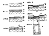
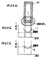
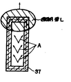
- 절연체 기판 또는 기본 반도체(30)상에 절연층(31)을 형성해서 되는 기판의 한 주면상에 다결정 또는 비정질의 반도체층(32)을 형성하는 제1의 공정과, 이 반도체층(32)에 대해 소정의 사진제판공정을 포함하는 가공 처리를 행하여 섬모양 반도체층(32)을 형성하는 제2의 공정과, 상기 섬모양 반도체층(32) 표면상에 또는 상기 표면상에 형성한 극히 얇은 실리콘 산화막(36)상에 얇은 실리콘 질화막(37)을 형성하는 제3의 공정과, 소정의 사진제판공정을 포함하는 가공 처리를 행하여 상기 섬모양 반도체층(32) 상면의 소정영역의 상기 실리콘 질화막(37)을 제거하는 제4의 공정과, 상기 섬모양 반도체층(32) 상면에 에너지선을 주사하면서 조사하여 상기 섬모양 반도체층(32)을 용융 재결정화 하여 상기 섬모양 반도체층(32)의 적어도 일부영역에 있어서, 단결정화 또는 결정입경을 증대시키는 제5의 공정을 구비한 것을 특징으로 하는 반도체 장치의 제조방법.
- 제1항에 있어서, 상기 제2의 공정은 상기 반도체층(32)상에 열산화막(33)을 형성하고, 상기 열산화막(33)상에 실리콘 질화막(34)을 형성하고, 이 실리콘 질화막(34)을 사진제판공정을 포함하는 가공 처리에 의해 섬모양 패턴으로 형성하고, 이것을 내산화분위기 마스크로서 상기 반도체층(32)을 산화하고, 상기 섬모양 실리콘 질화막(34)과 열산화막(33)을 제거하는 것을 특징으로 하는 반도체 장치의 제조방법.
- 제1항에 있어서, 상기 제2의 공정은 상기 반도체층(32)의 소정영역 이외를 리지스트 패턴에 따라 에칭하여 메사형의 섬모양 반도체층(32)을 형성하는 것을 특징으로 하는 반도체 장치의 제조방법.
- 제1항, 제2항 또는 제3항에 있어서, 상기 기본 반도체(30)는 실리콘인 것을 특징으로 하는 반도체 장치의 제조방법.
- 제1항, 제2항 또는 제3항에 있어서, 상기 다결정 또는 비정질의 반도체층(32)은 실리콘인 것을 특징으로 하는 반도체 장치의 제조방법.
- 제1항, 제2항 또는 제3항에 있어서, 상기 극히 얇은 실리콘 산화막(37)의 두께는 0 내지 200Å이고, 상기 얇은 실리콘 질화막의 두께는 400 내지 700Å인 것을 특징으로 하는 반도체 장치의 제조방법.
- 제4항에 있어서, 상기 다결정 또는 비정질의 반도체층(32)은 실리콘인 것을 특징으로 하는 반도체 장치의 제조방법.
- 제4항에 있어서, 상기 극히 얇은 실리콘 산화막(37)의 두께는 0 내지 200Å이고, 상기 얇은 실리콘 질화막의 두께는 400 내지 700Å인 것을 특징으로 하는 반도체 장치의 제조방법.
- 제5항에 있어서, 상기 극히 얇은 실리콘 산화막(37)의 두께는 0 내지 200Å이고, 상기 얇은 실리콘 질화막의 두께는 400 내지 700Å인 것을 특징으로 하는 반도체 장치의 제조방법.
Applications Claiming Priority (2)
| Application Number | Priority Date | Filing Date | Title |
|---|---|---|---|
| JP59006671A JPS60150618A (ja) | 1984-01-17 | 1984-01-17 | 半導体装置の製造方法 |
| JP6671 | 1984-01-17 |
Publications (2)
| Publication Number | Publication Date |
|---|---|
| KR850005729A KR850005729A (ko) | 1985-08-28 |
| KR900000061B1 true KR900000061B1 (ko) | 1990-01-19 |
Family
ID=11644831
Family Applications (1)
| Application Number | Title | Priority Date | Filing Date |
|---|---|---|---|
| KR1019840007513A Expired KR900000061B1 (ko) | 1984-01-17 | 1984-11-29 | 반도체 장치의 제조방법 |
Country Status (4)
| Country | Link |
|---|---|
| US (1) | US4661167A (ko) |
| JP (1) | JPS60150618A (ko) |
| KR (1) | KR900000061B1 (ko) |
| FR (1) | FR2560436B1 (ko) |
Families Citing this family (12)
| Publication number | Priority date | Publication date | Assignee | Title |
|---|---|---|---|---|
| EP0178447B1 (en) * | 1984-10-09 | 1993-02-17 | Fujitsu Limited | A manufacturing method of an integrated circuit based on semiconductor-on-insulator technology |
| EP0217179A3 (en) * | 1985-09-30 | 1989-05-31 | Allied Corporation | A method for laser crystallization of semiconductor islands on transparent substrates |
| JPH084067B2 (ja) * | 1985-10-07 | 1996-01-17 | 工業技術院長 | 半導体装置の製造方法 |
| JPS62179112A (ja) * | 1986-01-31 | 1987-08-06 | Nec Corp | Soi構造形成方法 |
| JPH0799734B2 (ja) * | 1986-10-31 | 1995-10-25 | 三菱電機株式会社 | 単結晶成長方法 |
| EP0449524B1 (en) * | 1990-03-24 | 1997-05-28 | Canon Kabushiki Kaisha | Optical annealing method for semiconductor layer and method for producing semiconductor device employing the same semiconductor layer |
| US5373803A (en) * | 1991-10-04 | 1994-12-20 | Sony Corporation | Method of epitaxial growth of semiconductor |
| JPH06177034A (ja) * | 1992-12-03 | 1994-06-24 | Sony Corp | 半導体単結晶の成長方法 |
| JPH0766420A (ja) * | 1993-08-31 | 1995-03-10 | Matsushita Electric Ind Co Ltd | 薄膜の加工方法 |
| TW589667B (en) * | 2001-09-25 | 2004-06-01 | Sharp Kk | Crystalline semiconductor film and production method thereof, and semiconductor device and production method thereof |
| US20040093263A1 (en) * | 2002-05-29 | 2004-05-13 | Doraisamy Malchiel A. | Automated Interview Method |
| US7168924B2 (en) * | 2002-09-27 | 2007-01-30 | Unico, Inc. | Rod pump control system including parameter estimator |
Family Cites Families (7)
| Publication number | Priority date | Publication date | Assignee | Title |
|---|---|---|---|---|
| JPS5814524A (ja) * | 1981-07-17 | 1983-01-27 | Fujitsu Ltd | 半導体装置の製造方法 |
| JPS58192381A (ja) * | 1982-05-06 | 1983-11-09 | Mitsubishi Electric Corp | Mos電界効果トランジスタの製造方法 |
| JPS59205712A (ja) * | 1983-04-30 | 1984-11-21 | Fujitsu Ltd | 半導体装置の製造方法 |
| US4592799A (en) * | 1983-05-09 | 1986-06-03 | Sony Corporation | Method of recrystallizing a polycrystalline, amorphous or small grain material |
| US4559102A (en) * | 1983-05-09 | 1985-12-17 | Sony Corporation | Method for recrystallizing a polycrystalline, amorphous or small grain material |
| JPS60117613A (ja) * | 1983-11-30 | 1985-06-25 | Fujitsu Ltd | 半導体装置の製造方法 |
| KR900001267B1 (ko) * | 1983-11-30 | 1990-03-05 | 후지쓰 가부시끼가이샤 | Soi형 반도체 장치의 제조방법 |
-
1984
- 1984-01-17 JP JP59006671A patent/JPS60150618A/ja active Pending
- 1984-11-29 KR KR1019840007513A patent/KR900000061B1/ko not_active Expired
- 1984-12-03 US US06/677,343 patent/US4661167A/en not_active Expired - Fee Related
-
1985
- 1985-01-17 FR FR8500647A patent/FR2560436B1/fr not_active Expired
Also Published As
| Publication number | Publication date |
|---|---|
| JPS60150618A (ja) | 1985-08-08 |
| FR2560436A1 (fr) | 1985-08-30 |
| KR850005729A (ko) | 1985-08-28 |
| FR2560436B1 (fr) | 1988-07-29 |
| US4661167A (en) | 1987-04-28 |
Similar Documents
| Publication | Publication Date | Title |
|---|---|---|
| US4514895A (en) | Method of forming field-effect transistors using selectively beam-crystallized polysilicon channel regions | |
| US4381201A (en) | Method for production of semiconductor devices | |
| KR910009038B1 (ko) | 절연물상 실리콘 구조를 갖는 고속 반도체 장치의 제조방법 | |
| US5310446A (en) | Method for producing semiconductor film | |
| KR900001266B1 (ko) | Soi형 반도체장치 제조방법 | |
| US5371381A (en) | Process for producing single crystal semiconductor layer and semiconductor device produced by said process | |
| KR900000061B1 (ko) | 반도체 장치의 제조방법 | |
| US5264072A (en) | Method for recrystallizing conductive films by an indirect-heating with a thermal-conduction-controlling layer | |
| US4414242A (en) | Process for fabricating a semiconductor device | |
| EP0225592B1 (en) | Recrystallizing conductive films | |
| US5510642A (en) | Semiconductor device | |
| US4861418A (en) | Method of manufacturing semiconductor crystalline layer | |
| US6664152B2 (en) | Method for crystallizing silicon film and thin film transistor and fabricating method using the same | |
| US4678538A (en) | Process for the production of an insulating support on an oriented monocrystalline silicon film with localized defects | |
| JPH0450746B2 (ko) | ||
| EP0575965B1 (en) | Method of forming semiconductor crystal and semiconductor device | |
| US4695856A (en) | Semiconductor device | |
| JPH0580159B2 (ko) | ||
| US5401683A (en) | Method of manufacturing a multi-layered semiconductor substrate | |
| JPS6159820A (ja) | 半導体装置の製造方法 | |
| JPS62219510A (ja) | 単結晶島状領域の形成方法 | |
| KR940006697B1 (ko) | Soi모스 제조방법 | |
| JPS6347253B2 (ko) | ||
| JPS61166074A (ja) | 絶縁ゲ−ト型トランジスタ及びその製造方法 | |
| JPH0223027B2 (ko) |
Legal Events
| Date | Code | Title | Description |
|---|---|---|---|
| PA0109 | Patent application |
St.27 status event code: A-0-1-A10-A12-nap-PA0109 |
|
| R17-X000 | Change to representative recorded |
St.27 status event code: A-3-3-R10-R17-oth-X000 |
|
| PG1501 | Laying open of application |
St.27 status event code: A-1-1-Q10-Q12-nap-PG1501 |
|
| A201 | Request for examination | ||
| P11-X000 | Amendment of application requested |
St.27 status event code: A-2-2-P10-P11-nap-X000 |
|
| P13-X000 | Application amended |
St.27 status event code: A-2-2-P10-P13-nap-X000 |
|
| PA0201 | Request for examination |
St.27 status event code: A-1-2-D10-D11-exm-PA0201 |
|
| G160 | Decision to publish patent application | ||
| PG1605 | Publication of application before grant of patent |
St.27 status event code: A-2-2-Q10-Q13-nap-PG1605 |
|
| E701 | Decision to grant or registration of patent right | ||
| PE0701 | Decision of registration |
St.27 status event code: A-1-2-D10-D22-exm-PE0701 |
|
| GRNT | Written decision to grant | ||
| PR0701 | Registration of establishment |
St.27 status event code: A-2-4-F10-F11-exm-PR0701 |
|
| PR1002 | Payment of registration fee |
St.27 status event code: A-2-2-U10-U11-oth-PR1002 Fee payment year number: 1 |
|
| PR1001 | Payment of annual fee |
St.27 status event code: A-4-4-U10-U11-oth-PR1001 Fee payment year number: 4 |
|
| PR1001 | Payment of annual fee |
St.27 status event code: A-4-4-U10-U11-oth-PR1001 Fee payment year number: 5 |
|
| PR1001 | Payment of annual fee |
St.27 status event code: A-4-4-U10-U11-oth-PR1001 Fee payment year number: 6 |
|
| FPAY | Annual fee payment |
Payment date: 19960116 Year of fee payment: 7 |
|
| PR1001 | Payment of annual fee |
St.27 status event code: A-4-4-U10-U11-oth-PR1001 Fee payment year number: 7 |
|
| LAPS | Lapse due to unpaid annual fee | ||
| PC1903 | Unpaid annual fee |
St.27 status event code: A-4-4-U10-U13-oth-PC1903 Not in force date: 19970120 Payment event data comment text: Termination Category : DEFAULT_OF_REGISTRATION_FEE |
|
| PN2301 | Change of applicant |
St.27 status event code: A-5-5-R10-R13-asn-PN2301 St.27 status event code: A-5-5-R10-R11-asn-PN2301 |
|
| PN2301 | Change of applicant |
St.27 status event code: A-5-5-R10-R13-asn-PN2301 St.27 status event code: A-5-5-R10-R11-asn-PN2301 |
|
| R18-X000 | Changes to party contact information recorded |
St.27 status event code: A-5-5-R10-R18-oth-X000 |
|
| PN2301 | Change of applicant |
St.27 status event code: A-5-5-R10-R13-asn-PN2301 St.27 status event code: A-5-5-R10-R11-asn-PN2301 |
|
| PC1903 | Unpaid annual fee |
St.27 status event code: N-4-6-H10-H13-oth-PC1903 Ip right cessation event data comment text: Termination Category : DEFAULT_OF_REGISTRATION_FEE Not in force date: 19970120 |
|
| R18-X000 | Changes to party contact information recorded |
St.27 status event code: A-5-5-R10-R18-oth-X000 |
|
| PN2301 | Change of applicant |
St.27 status event code: A-5-5-R10-R13-asn-PN2301 St.27 status event code: A-5-5-R10-R11-asn-PN2301 |
|
| P22-X000 | Classification modified |
St.27 status event code: A-4-4-P10-P22-nap-X000 |
|
| P22-X000 | Classification modified |
St.27 status event code: A-4-4-P10-P22-nap-X000 |
|
| P22-X000 | Classification modified |
St.27 status event code: A-4-4-P10-P22-nap-X000 |