KR900000063B1 - 반도체 집적회로에 사용된 반도체 저항요소 - Google Patents
반도체 집적회로에 사용된 반도체 저항요소 Download PDFInfo
- Publication number
- KR900000063B1 KR900000063B1 KR1019860004152A KR860004152A KR900000063B1 KR 900000063 B1 KR900000063 B1 KR 900000063B1 KR 1019860004152 A KR1019860004152 A KR 1019860004152A KR 860004152 A KR860004152 A KR 860004152A KR 900000063 B1 KR900000063 B1 KR 900000063B1
- Authority
- KR
- South Korea
- Prior art keywords
- fet
- gate
- drain
- voltage
- resistive element
- Prior art date
- Legal status (The legal status is an assumption and is not a legal conclusion. Google has not performed a legal analysis and makes no representation as to the accuracy of the status listed.)
- Expired
Links
Images


Classifications
-
- H—ELECTRICITY
- H10—SEMICONDUCTOR DEVICES; ELECTRIC SOLID-STATE DEVICES NOT OTHERWISE PROVIDED FOR
- H10D—INORGANIC ELECTRIC SEMICONDUCTOR DEVICES
- H10D84/00—Integrated devices formed in or on semiconductor substrates that comprise only semiconducting layers, e.g. on Si wafers or on GaAs-on-Si wafers
- H10D84/01—Manufacture or treatment
- H10D84/02—Manufacture or treatment characterised by using material-based technologies
- H10D84/05—Manufacture or treatment characterised by using material-based technologies using Group III-V technology
Landscapes
- Junction Field-Effect Transistors (AREA)
- Semiconductor Integrated Circuits (AREA)
- Logic Circuits (AREA)
Abstract
Description
Claims (10)
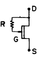
- 각각이 반도체 기판상에 형성된 소트키 게이트형 FET 또는 접합형 게이트형 FET를 포함하는 반도체 집적회로에 사용된 반도체 저항요소에 있어서, 여기에서 상기 저항요소가 상호연결된 드레인과 게이트 전극을 가지는 상기 FET로 구성되고, 드레인-소오스 전압 VDS가 게이트와 드레인 전극사이 형성된 다이오드의 순방향 상승전압 VF이하로 되도록 제한하기 위하여 그것의 드레인 전류 IDS를 제한하는 것을 특징으로 하는 반도체 저항요소.
- 청구버위 제1항에 있어서, 반도체 저항요소로서 사용된 FET가 쇼트키 접촉에 의하여 반도체 절연기판(semi- insulating Substratl)에 형성된 액티브층과 접하여 유지된 게이트 전극을 가지는 MESFET인 반도체 저항요소.
- 청구범위 제1항에 있어서, 반도체 저항요소로서 사용된 FET가 PN접촉에 의하여 액티브 층과 접하여 유지된 게이트 전극을 가지는 접합형 FET인 반도체 저항요소.
- 청구범위 제1항에 있어서, 반도체 저항요소로서 사용된 FET가 이종접합에 의하여 반도체 층과 접하여 유지된 게이트 전극을 가지는 접합형 FET인 반도체 저항요소.
- 청구범위 제1항에 있어서, 반도체 저항요소로서 사용된 FET가 액티브요소로서 사용되는 FET의 제조공정중에 함께 기판상에 형성된 반도체 저항요소.
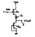
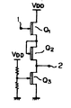
- 집적회로에 사용된 레벨 쉬프트회로에 있어서, 입력전압 Vin이 공급되는 게이트 전극을 가지는 첫 번째 FET Q1정전류원으로서 작용하는 두 번째 FET Q3, 상호연결된 드레인과 게이트전극을 가지는 쇼트키 게이트형 FET 또는 접합 게이트형 FET Q2로 구성되고, 드레인-소오스 전압 VDS이 게이트와 드레인 전극사이에 형성된 다이오드의 순방향 상승전압 VF이하로 되도록 제한하기 위하여 그것의 드레인 전류 IDS가 제한되는 반도체 저항 요소를 가지며, 여기에서 첫 번째와 두 번째 VF와 그들사이에 놓여진 반도체 저항 요소 Q2가 전원전압 VDD과 접지 사이에 직렬로 연결되는 것을 특징으로 하는 레벨 쉬프트회로.(제3도)
- 청구범위 제6항에 있어서, 첫 번째와 두 번째 FET Q1과 Q3이 동일 특성을 가지도록 동일 제조 공정중에 형성되는 레벨 쉬프트 회로.
- 청구범위 제6항에 있어서, 두 번째 FET Q3의 드레인과 게이트 전극이 정전류원으로서 동작 하기 위하여 폐회로화 되는 레벨 쉬프트 회로.
- 청구범위 제6항에 있어서, 두 번째 FET Q3의 게이트 전극이 저항전압 분할기에 의하여 정전압으로 바이어스되는 레벨쉬프트 회로.
- 청구범위 제6항에 있어서, 반도체 저항요소를 통하여 흐르는 전류가 다음식에 기초하여 반도체 저항요소로서 FET의 게이트 폭을 정하므로서 결정되며,
 여기에서 VF는 FET의 드레인과 게이트 전극사이의 다이오드의 dc순반향 전압이고, Vth는 FET의 드레쉬 홀드 전압, WG3는 두 번째 FET의 게이트 폭, WD2는 반도체 저항요소로서 FET의 게이트폭인 레벨 쉬프트회로.
Applications Claiming Priority (3)
| Application Number | Priority Date | Filing Date | Title |
|---|---|---|---|
| JP60-115855 | 1985-05-28 | ||
| JP115855 | 1985-05-28 | ||
| JP60115855A JPS61272964A (ja) | 1985-05-28 | 1985-05-28 | 半導体抵抗素子 |
Publications (2)
| Publication Number | Publication Date |
|---|---|
| KR860009493A KR860009493A (ko) | 1986-12-23 |
| KR900000063B1 true KR900000063B1 (ko) | 1990-01-19 |
Family
ID=14672805
Family Applications (1)
| Application Number | Title | Priority Date | Filing Date |
|---|---|---|---|
| KR1019860004152A Expired KR900000063B1 (ko) | 1985-05-28 | 1986-05-27 | 반도체 집적회로에 사용된 반도체 저항요소 |
Country Status (5)
| Country | Link |
|---|---|
| US (1) | US4810907A (ko) |
| EP (1) | EP0222467B1 (ko) |
| JP (1) | JPS61272964A (ko) |
| KR (1) | KR900000063B1 (ko) |
| DE (1) | DE3673605D1 (ko) |
Families Citing this family (16)
| Publication number | Priority date | Publication date | Assignee | Title |
|---|---|---|---|---|
| US4760284A (en) * | 1987-01-12 | 1988-07-26 | Triquint Semiconductor, Inc. | Pinchoff voltage generator |
| JPH0793410B2 (ja) * | 1987-12-28 | 1995-10-09 | 三菱電機株式会社 | 半導体装置 |
| US5010385A (en) * | 1990-03-30 | 1991-04-23 | The United States Of America As Represented By The Secretary Of The Navy | Resistive element using depletion-mode MOSFET's |
| US5359301A (en) * | 1993-03-26 | 1994-10-25 | National Semiconductor Corporation | Process-, temperature-, and voltage-compensation for ECL delay cells |
| JP3305827B2 (ja) * | 1993-09-07 | 2002-07-24 | 株式会社東芝 | 半導体集積回路 |
| JP3400853B2 (ja) * | 1994-04-27 | 2003-04-28 | 三菱電機株式会社 | 半導体装置 |
| SG83670A1 (en) * | 1997-09-02 | 2001-10-16 | Oki Techno Ct Singapore | A bias stabilization circuit |
| US6111430A (en) * | 1998-06-24 | 2000-08-29 | International Business Machines Corporation | Circuit for interfacing a first type of logic circuit with a second type of logic circuit |
| US6864131B2 (en) * | 1999-06-02 | 2005-03-08 | Arizona State University | Complementary Schottky junction transistors and methods of forming the same |
| US7589007B2 (en) * | 1999-06-02 | 2009-09-15 | Arizona Board Of Regents For And On Behalf Of Arizona State University | MESFETs integrated with MOSFETs on common substrate and methods of forming the same |
| JP2003086767A (ja) * | 2001-09-14 | 2003-03-20 | Matsushita Electric Ind Co Ltd | 半導体装置 |
| US6788136B2 (en) * | 2001-10-25 | 2004-09-07 | General Electric Company | Methods and apparatus for amplification in high temperature environments |
| US6781417B1 (en) * | 2002-10-29 | 2004-08-24 | Advanced Micro Devices, Inc. | Buffer driver circuit for producing a fast, stable, and accurate reference voltage |
| US7183593B2 (en) * | 2003-12-05 | 2007-02-27 | Taiwan Semiconductor Manufacturing Company, Ltd. | Heterostructure resistor and method of forming the same |
| US7746146B2 (en) * | 2006-07-28 | 2010-06-29 | Suvolta, Inc. | Junction field effect transistor input buffer level shifting circuit |
| WO2011107161A1 (en) * | 2010-03-05 | 2011-09-09 | Epcos Ag | Resistance component |
Family Cites Families (3)
| Publication number | Priority date | Publication date | Assignee | Title |
|---|---|---|---|---|
| US4400636A (en) * | 1980-12-05 | 1983-08-23 | Ibm Corporation | Threshold voltage tolerant logic |
| US4423339A (en) * | 1981-02-23 | 1983-12-27 | Motorola, Inc. | Majority logic gate |
| US4631426A (en) * | 1984-06-27 | 1986-12-23 | Honeywell Inc. | Digital circuit using MESFETS |
-
1985
- 1985-05-28 JP JP60115855A patent/JPS61272964A/ja active Pending
-
1986
- 1986-05-27 KR KR1019860004152A patent/KR900000063B1/ko not_active Expired
- 1986-05-28 EP EP86304057A patent/EP0222467B1/en not_active Expired - Lifetime
- 1986-05-28 DE DE8686304057T patent/DE3673605D1/de not_active Expired - Lifetime
-
1988
- 1988-07-01 US US07/221,019 patent/US4810907A/en not_active Expired - Lifetime
Also Published As
| Publication number | Publication date |
|---|---|
| JPS61272964A (ja) | 1986-12-03 |
| EP0222467A1 (en) | 1987-05-20 |
| EP0222467B1 (en) | 1990-08-22 |
| US4810907A (en) | 1989-03-07 |
| DE3673605D1 (de) | 1990-09-27 |
| KR860009493A (ko) | 1986-12-23 |
Similar Documents
| Publication | Publication Date | Title |
|---|---|---|
| KR900000063B1 (ko) | 반도체 집적회로에 사용된 반도체 저항요소 | |
| Yang et al. | New method to measure the source and drain resistance of the GaAs MESFET | |
| EP0045841B1 (en) | Linear voltage-current converter | |
| EP0585755A1 (en) | Apparatus and method providing a MOS temperature compensated voltage reference for low voltages and wide voltage ranges | |
| US4394589A (en) | Logic circuit including at least one resistor or one transistor having a saturable resistor field effect transistor structure | |
| JPH05187926A (ja) | 温度検知回路 | |
| EP0442413A2 (en) | E/D integrated circuit formed in compound semiconductor substrate | |
| US4423339A (en) | Majority logic gate | |
| US6255897B1 (en) | Current biasing circuit | |
| JP2753266B2 (ja) | 半導体回路 | |
| EP0176754A1 (en) | Schottky-gate field effect transistor | |
| US12484245B2 (en) | Power device with current sense | |
| US4760284A (en) | Pinchoff voltage generator | |
| US4937517A (en) | Constant current source circuit | |
| US4661726A (en) | Utilizing a depletion mode FET operating in the triode region and a depletion mode FET operating in the saturation region | |
| EP0200230A2 (en) | Logic integrated circuit device formed on compound semiconductor substrate | |
| US20070040226A1 (en) | Cascode circuit | |
| KR970005290B1 (ko) | 증폭기 회로 | |
| US4975631A (en) | Constant current source circuit | |
| RU2069448C1 (ru) | Усилитель | |
| DE102023134219B4 (de) | Leistungsgerät mit Strommessung | |
| Peczalski et al. | Modeling and characterization of ion-implanted GaAs MESFET's | |
| JPH06265584A (ja) | 半導体装置 | |
| JPH0336111Y2 (ko) | ||
| JP2943221B2 (ja) | 半導体装置 |
Legal Events
| Date | Code | Title | Description |
|---|---|---|---|
| A201 | Request for examination | ||
| PA0109 | Patent application |
St.27 status event code: A-0-1-A10-A12-nap-PA0109 |
|
| PA0201 | Request for examination |
St.27 status event code: A-1-2-D10-D11-exm-PA0201 |
|
| R17-X000 | Change to representative recorded |
St.27 status event code: A-3-3-R10-R17-oth-X000 |
|
| PG1501 | Laying open of application |
St.27 status event code: A-1-1-Q10-Q12-nap-PG1501 |
|
| G160 | Decision to publish patent application | ||
| PG1605 | Publication of application before grant of patent |
St.27 status event code: A-2-2-Q10-Q13-nap-PG1605 |
|
| E701 | Decision to grant or registration of patent right | ||
| PE0701 | Decision of registration |
St.27 status event code: A-1-2-D10-D22-exm-PE0701 |
|
| GRNT | Written decision to grant | ||
| PR0701 | Registration of establishment |
St.27 status event code: A-2-4-F10-F11-exm-PR0701 |
|
| PR1002 | Payment of registration fee |
St.27 status event code: A-2-2-U10-U11-oth-PR1002 Fee payment year number: 1 |
|
| FPAY | Annual fee payment |
Payment date: 19921214 Year of fee payment: 4 |
|
| PR1001 | Payment of annual fee |
St.27 status event code: A-4-4-U10-U11-oth-PR1001 Fee payment year number: 4 |
|
| LAPS | Lapse due to unpaid annual fee | ||
| PC1903 | Unpaid annual fee |
St.27 status event code: A-4-4-U10-U13-oth-PC1903 Not in force date: 19940120 Payment event data comment text: Termination Category : DEFAULT_OF_REGISTRATION_FEE |
|
| PC1903 | Unpaid annual fee |
St.27 status event code: N-4-6-H10-H13-oth-PC1903 Ip right cessation event data comment text: Termination Category : DEFAULT_OF_REGISTRATION_FEE Not in force date: 19940120 |
|
| PN2301 | Change of applicant |
St.27 status event code: A-5-5-R10-R13-asn-PN2301 St.27 status event code: A-5-5-R10-R11-asn-PN2301 |
|
| PN2301 | Change of applicant |
St.27 status event code: A-5-5-R10-R13-asn-PN2301 St.27 status event code: A-5-5-R10-R11-asn-PN2301 |
|
| R18-X000 | Changes to party contact information recorded |
St.27 status event code: A-5-5-R10-R18-oth-X000 |
|
| R18-X000 | Changes to party contact information recorded |
St.27 status event code: A-5-5-R10-R18-oth-X000 |
|
| PN2301 | Change of applicant |
St.27 status event code: A-5-5-R10-R13-asn-PN2301 St.27 status event code: A-5-5-R10-R11-asn-PN2301 |
|
| P22-X000 | Classification modified |
St.27 status event code: A-4-4-P10-P22-nap-X000 |
|
| P22-X000 | Classification modified |
St.27 status event code: A-4-4-P10-P22-nap-X000 |