KR900000068B1 - 반도체 장치 - Google Patents
반도체 장치 Download PDFInfo
- Publication number
- KR900000068B1 KR900000068B1 KR1019860006562A KR860006562A KR900000068B1 KR 900000068 B1 KR900000068 B1 KR 900000068B1 KR 1019860006562 A KR1019860006562 A KR 1019860006562A KR 860006562 A KR860006562 A KR 860006562A KR 900000068 B1 KR900000068 B1 KR 900000068B1
- Authority
- KR
- South Korea
- Prior art keywords
- gate
- short
- field effect
- circuit
- effect transistor
- Prior art date
- Legal status (The legal status is an assumption and is not a legal conclusion. Google has not performed a legal analysis and makes no representation as to the accuracy of the status listed.)
- Expired
Links
Images


Classifications
-
- H—ELECTRICITY
- H03—ELECTRONIC CIRCUITRY
- H03K—PULSE TECHNIQUE
- H03K19/00—Logic circuits, i.e. having at least two inputs acting on one output; Inverting circuits
- H03K19/01—Modifications for accelerating switching
- H03K19/017—Modifications for accelerating switching in field-effect transistor circuits
- H03K19/01707—Modifications for accelerating switching in field-effect transistor circuits in asynchronous circuits
- H03K19/01714—Modifications for accelerating switching in field-effect transistor circuits in asynchronous circuits by bootstrapping, i.e. by positive feed-back
-
- H—ELECTRICITY
- H03—ELECTRONIC CIRCUITRY
- H03K—PULSE TECHNIQUE
- H03K19/00—Logic circuits, i.e. having at least two inputs acting on one output; Inverting circuits
- H03K19/02—Logic circuits, i.e. having at least two inputs acting on one output; Inverting circuits using specified components
- H03K19/08—Logic circuits, i.e. having at least two inputs acting on one output; Inverting circuits using specified components using semiconductor devices
- H03K19/094—Logic circuits, i.e. having at least two inputs acting on one output; Inverting circuits using specified components using semiconductor devices using field-effect transistors
- H03K19/0952—Logic circuits, i.e. having at least two inputs acting on one output; Inverting circuits using specified components using semiconductor devices using field-effect transistors using Schottky type FET MESFET
Landscapes
- Engineering & Computer Science (AREA)
- Physics & Mathematics (AREA)
- Computer Hardware Design (AREA)
- Computing Systems (AREA)
- General Engineering & Computer Science (AREA)
- Mathematical Physics (AREA)
- Power Engineering (AREA)
- Logic Circuits (AREA)
- Junction Field-Effect Transistors (AREA)
Abstract
Description
Claims (7)
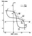
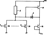
- 제1전위에 접속된 하나의 단자를 가지는 부하(8)과, 상기 부하의 다른 단자와 그 게이트에서 외부로부터 인가된 입력신호를 수신하는 제2전위간에 접속된 제1쇼트기게이트 전계효과트랜지스터(9)와, 상기 제1전위에 접속된 하나의 전도단자 및 상기 제1쇼트기 게이트전계효과트랜지스터(9)와 상기 부하(8)의 노우드에 접속된 게이트를 가지는 제2쇼트기게이트전계효과트랜지스터(10)과, 상기 제2쇼트기게이트전계효과트랜지스터(10)의 다른 전도단자에 접속된 하나의 전도단자와 제3전위에 접속된 게이트 및 다른 전도단자를 가지는 제3쇼트기게이트전계효과트랜지스터(12)와, 상기 제2쇼트기게이트전계효과트랜지스터(10)의 게이트에 접속된 음극과 상기 제2쇼트기게이트전계효과트랜지스터(10)의 다른 전도 단자에 접속된 양극을 가지는 쇼트기베리어다이오우드(11)로 구성되는 화합물반도체를 이용하여 제조된 반도체장치.
- 제1항에 있어서, 상기 화합물반도체는 갈륨비화물인것을 특징으로 하는 반도체장치.
- 제1항에 있어서, 상기 제2쇼트기게이트전계효과트랜지스터(10)의 게이트폭은 상기 제3쇼트기게이트전계효과트랜지스터(12)의 게이트폭보다 작게하는 것을 특징으로 하는 반도체장치.
- 제1항에 있어서, 상기 제2쇼트기게이트전계효과트랜지스터(10)의 임계전압의 절대값은 상기 제3쇼트기게이트전계효과트랜지스터(12)의 임계전압의 절대값보다 작게하는 것을 특징으로 하는 반도체장치.
- 제1항에 있어서, 상기 제1쇼트기게이트전계효과트랜지스터(9)는 단일 쇼트기게이트전계효과트랜지스터(9) 인것을 특징으로 하는 반도체장치.
- 제1항에 있어서, 상기 제1쇼트기게이트전계효과트랜지스터(9)는 상기 부하의 상기 다른 전도단자와 각 게이트에서 입력신호를 수신하는 상기 제2전위간에 상호 병렬로 접속된 복수의 쇼트기게이트전계효과트랜지스터(9a 내지 9n)로 구성되는 것을 특징으로 하는 반도체장치.
- 제1항에 있어서, 상기 제1쇼트기게이트전계효과트랜지스터는 상기 부하의 상기 다른 전도단자와 각 게이트에서 입력신호를 수신하는 상기 제2전위간에 서로 직렬로 접속된 복수의 쇼트기게이트전계효과트랜지스터(9a 내지 9n)로 구성되는 것을 특징으로 하는 반도체장치.
Applications Claiming Priority (3)
| Application Number | Priority Date | Filing Date | Title |
|---|---|---|---|
| JP176587 | 1985-08-09 | ||
| JP60176587A JPS6297427A (ja) | 1985-08-09 | 1985-08-09 | 半導体装置 |
| JP60-176587 | 1985-08-09 |
Publications (2)
| Publication Number | Publication Date |
|---|---|
| KR870002662A KR870002662A (ko) | 1987-04-06 |
| KR900000068B1 true KR900000068B1 (ko) | 1990-01-19 |
Family
ID=16016168
Family Applications (1)
| Application Number | Title | Priority Date | Filing Date |
|---|---|---|---|
| KR1019860006562A Expired KR900000068B1 (ko) | 1985-08-09 | 1986-08-09 | 반도체 장치 |
Country Status (5)
| Country | Link |
|---|---|
| US (1) | US4755695A (ko) |
| EP (1) | EP0217072A1 (ko) |
| JP (1) | JPS6297427A (ko) |
| KR (1) | KR900000068B1 (ko) |
| CA (1) | CA1260561A (ko) |
Families Citing this family (10)
| Publication number | Priority date | Publication date | Assignee | Title |
|---|---|---|---|---|
| US4900953A (en) * | 1987-03-11 | 1990-02-13 | Fujitsu Limited | Logic circuit employing field effect transistor having junction with rectifying characteristic between gate and source |
| GB8718654D0 (en) * | 1987-08-06 | 1987-09-09 | Plessey Co Plc | Transistor switching circuits |
| US4868427A (en) * | 1987-10-30 | 1989-09-19 | Gazelle Microcircuits, Inc. | ECL to TTL circuit |
| US5027007A (en) * | 1989-04-12 | 1991-06-25 | The Boeing Company | FFL/QFL FET logic circuits |
| US5182473A (en) * | 1990-07-31 | 1993-01-26 | Cray Research, Inc. | Emitter emitter logic (EEL) and emitter collector dotted logic (ECDL) families |
| KR930006629B1 (ko) * | 1990-08-06 | 1993-07-21 | 재단법인 한국전자통신연구소 | 저 소비전력형 워드선 구동회로 |
| JP2007227625A (ja) * | 2006-02-23 | 2007-09-06 | Toshiba Microelectronics Corp | 半導体集積回路及びそのレイアウト設計方法 |
| JP5015029B2 (ja) * | 2007-03-09 | 2012-08-29 | パナソニック株式会社 | 昇圧回路に用いられる電流制御回路 |
| DE102010004488B3 (de) * | 2010-01-12 | 2011-06-16 | Thales Defence Deutschland Gmbh | Pegelwandlerschaltung |
| US9190993B1 (en) * | 2015-01-08 | 2015-11-17 | United Silicon Carbide, Inc. | High voltage switch |
Family Cites Families (3)
| Publication number | Priority date | Publication date | Assignee | Title |
|---|---|---|---|---|
| FR2264434B1 (ko) * | 1974-03-12 | 1976-07-16 | Thomson Csf | |
| JPS5856531A (ja) * | 1981-09-30 | 1983-04-04 | Toshiba Corp | 論理回路 |
| US4558235A (en) * | 1983-08-31 | 1985-12-10 | Texas Instruments Incorporated | MESFET logic gate having both DC and AC level shift coupling to the output |
-
1985
- 1985-08-09 JP JP60176587A patent/JPS6297427A/ja active Pending
-
1986
- 1986-08-05 US US06/893,496 patent/US4755695A/en not_active Expired - Fee Related
- 1986-08-06 EP EP86110881A patent/EP0217072A1/en not_active Withdrawn
- 1986-08-09 KR KR1019860006562A patent/KR900000068B1/ko not_active Expired
- 1986-08-11 CA CA000515705A patent/CA1260561A/en not_active Expired
Also Published As
| Publication number | Publication date |
|---|---|
| JPS6297427A (ja) | 1987-05-06 |
| US4755695A (en) | 1988-07-05 |
| EP0217072A1 (en) | 1987-04-08 |
| CA1260561A (en) | 1989-09-26 |
| KR870002662A (ko) | 1987-04-06 |
Similar Documents
| Publication | Publication Date | Title |
|---|---|---|
| KR940001251B1 (ko) | 전압 제어회로 | |
| US5444396A (en) | Level shifting circuit | |
| EP0100213B1 (en) | Gallium arsenide vlsi chip | |
| KR920001634B1 (ko) | 중간전위 발생회로 | |
| US7504876B1 (en) | Substrate bias feedback scheme to reduce chip leakage power | |
| KR920005358B1 (ko) | 버퍼회로 | |
| JP2549743B2 (ja) | 出力回路 | |
| EP0053664B1 (en) | Integrated logic gate | |
| US4701643A (en) | FET gate current limiter circuits | |
| KR900000068B1 (ko) | 반도체 장치 | |
| KR900009192B1 (ko) | 차동회로 | |
| US5148244A (en) | Enhancement-fet and depletion-fet with different gate length formed in compound semiconductor substrate | |
| US4713559A (en) | Multiple input and multiple output or/and circuit | |
| KR920005359B1 (ko) | 논리 레벨 변환용 버퍼회로. | |
| EP0562719B1 (en) | An integrated circuit device made by compound semiconductor | |
| KR100241201B1 (ko) | 버스홀드회로 | |
| US4967105A (en) | Load current control-type logic circuit | |
| US4924116A (en) | Feedback source coupled FET logic | |
| JPS6070822A (ja) | 半導体集積回路 | |
| JP3255874B2 (ja) | 定電流回路 | |
| US4380707A (en) | Transistor-transistor logic input buffer circuit with power supply/temperature effects compensation circuit | |
| US4996447A (en) | Field-effect transistor load circuit | |
| US4752701A (en) | Direct coupled semiconductor logic circuit | |
| GB2166312A (en) | Capacitor diode level shift circuit | |
| US20050134331A1 (en) | Input buffer circuit including reference voltage monitoring circuit |
Legal Events
| Date | Code | Title | Description |
|---|---|---|---|
| A201 | Request for examination | ||
| PA0109 | Patent application |
St.27 status event code: A-0-1-A10-A12-nap-PA0109 |
|
| PA0201 | Request for examination |
St.27 status event code: A-1-2-D10-D11-exm-PA0201 |
|
| R17-X000 | Change to representative recorded |
St.27 status event code: A-3-3-R10-R17-oth-X000 |
|
| P11-X000 | Amendment of application requested |
St.27 status event code: A-2-2-P10-P11-nap-X000 |
|
| P13-X000 | Application amended |
St.27 status event code: A-2-2-P10-P13-nap-X000 |
|
| PG1501 | Laying open of application |
St.27 status event code: A-1-1-Q10-Q12-nap-PG1501 |
|
| G160 | Decision to publish patent application | ||
| PG1605 | Publication of application before grant of patent |
St.27 status event code: A-2-2-Q10-Q13-nap-PG1605 |
|
| E701 | Decision to grant or registration of patent right | ||
| PE0701 | Decision of registration |
St.27 status event code: A-1-2-D10-D22-exm-PE0701 |
|
| GRNT | Written decision to grant | ||
| PR0701 | Registration of establishment |
St.27 status event code: A-2-4-F10-F11-exm-PR0701 |
|
| PR1002 | Payment of registration fee |
St.27 status event code: A-2-2-U10-U11-oth-PR1002 Fee payment year number: 1 |
|
| PR1001 | Payment of annual fee |
St.27 status event code: A-4-4-U10-U11-oth-PR1001 Fee payment year number: 4 |
|
| PR1001 | Payment of annual fee |
St.27 status event code: A-4-4-U10-U11-oth-PR1001 Fee payment year number: 5 |
|
| PR1001 | Payment of annual fee |
St.27 status event code: A-4-4-U10-U11-oth-PR1001 Fee payment year number: 6 |
|
| PR1001 | Payment of annual fee |
St.27 status event code: A-4-4-U10-U11-oth-PR1001 Fee payment year number: 7 |
|
| FPAY | Annual fee payment |
Payment date: 19961230 Year of fee payment: 8 |
|
| PR1001 | Payment of annual fee |
St.27 status event code: A-4-4-U10-U11-oth-PR1001 Fee payment year number: 8 |
|
| LAPS | Lapse due to unpaid annual fee | ||
| PC1903 | Unpaid annual fee |
St.27 status event code: A-4-4-U10-U13-oth-PC1903 Not in force date: 19980120 Payment event data comment text: Termination Category : DEFAULT_OF_REGISTRATION_FEE |
|
| PC1903 | Unpaid annual fee |
St.27 status event code: N-4-6-H10-H13-oth-PC1903 Ip right cessation event data comment text: Termination Category : DEFAULT_OF_REGISTRATION_FEE Not in force date: 19980120 |
|
| PN2301 | Change of applicant |
St.27 status event code: A-5-5-R10-R13-asn-PN2301 St.27 status event code: A-5-5-R10-R11-asn-PN2301 |
|
| P22-X000 | Classification modified |
St.27 status event code: A-4-4-P10-P22-nap-X000 |
|
| P22-X000 | Classification modified |
St.27 status event code: A-4-4-P10-P22-nap-X000 |
|
| R18-X000 | Changes to party contact information recorded |
St.27 status event code: A-5-5-R10-R18-oth-X000 |