KR900000069B1 - 반도체 장치 - Google Patents
반도체 장치 Download PDFInfo
- Publication number
- KR900000069B1 KR900000069B1 KR8203475A KR820003475A KR900000069B1 KR 900000069 B1 KR900000069 B1 KR 900000069B1 KR 8203475 A KR8203475 A KR 8203475A KR 820003475 A KR820003475 A KR 820003475A KR 900000069 B1 KR900000069 B1 KR 900000069B1
- Authority
- KR
- South Korea
- Prior art keywords
- pellet
- protective film
- pellets
- wire bonding
- insulating protective
- Prior art date
- Legal status (The legal status is an assumption and is not a legal conclusion. Google has not performed a legal analysis and makes no representation as to the accuracy of the status listed.)
- Expired
Links
Images



Classifications
-
- H—ELECTRICITY
- H10—SEMICONDUCTOR DEVICES; ELECTRIC SOLID-STATE DEVICES NOT OTHERWISE PROVIDED FOR
- H10W—GENERIC PACKAGES, INTERCONNECTIONS, CONNECTORS OR OTHER CONSTRUCTIONAL DETAILS OF DEVICES COVERED BY CLASS H10
- H10W72/00—Interconnections or connectors in packages
- H10W72/50—Bond wires
-
- H—ELECTRICITY
- H10—SEMICONDUCTOR DEVICES; ELECTRIC SOLID-STATE DEVICES NOT OTHERWISE PROVIDED FOR
- H10W—GENERIC PACKAGES, INTERCONNECTIONS, CONNECTORS OR OTHER CONSTRUCTIONAL DETAILS OF DEVICES COVERED BY CLASS H10
- H10W46/00—Marks applied to devices, e.g. for alignment or identification
-
- H—ELECTRICITY
- H10—SEMICONDUCTOR DEVICES; ELECTRIC SOLID-STATE DEVICES NOT OTHERWISE PROVIDED FOR
- H10W—GENERIC PACKAGES, INTERCONNECTIONS, CONNECTORS OR OTHER CONSTRUCTIONAL DETAILS OF DEVICES COVERED BY CLASS H10
- H10W72/00—Interconnections or connectors in packages
- H10W72/90—Bond pads, in general
Landscapes
- Testing Or Measuring Of Semiconductors Or The Like (AREA)
- Wire Bonding (AREA)
Abstract
Description


Claims (1)
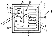
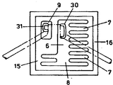
- 기판(2)에 고착한 반도체 펠릿(3)위에 와이어 본딩 위치에 패턴 인식위치 결정용의 절연보호막제 마아킹(11), (12), (13), (14), (30), (31)을 설치한 것을 특징으로 하는 반도체 장치.
Priority Applications (1)
| Application Number | Priority Date | Filing Date | Title |
|---|---|---|---|
| KR8203475A KR900000069B1 (ko) | 1982-08-03 | 1982-08-03 | 반도체 장치 |
Applications Claiming Priority (1)
| Application Number | Priority Date | Filing Date | Title |
|---|---|---|---|
| KR8203475A KR900000069B1 (ko) | 1982-08-03 | 1982-08-03 | 반도체 장치 |
Publications (2)
| Publication Number | Publication Date |
|---|---|
| KR840001387A KR840001387A (ko) | 1984-04-30 |
| KR900000069B1 true KR900000069B1 (ko) | 1990-01-19 |
Family
ID=19225285
Family Applications (1)
| Application Number | Title | Priority Date | Filing Date |
|---|---|---|---|
| KR8203475A Expired KR900000069B1 (ko) | 1982-08-03 | 1982-08-03 | 반도체 장치 |
Country Status (1)
| Country | Link |
|---|---|
| KR (1) | KR900000069B1 (ko) |
-
1982
- 1982-08-03 KR KR8203475A patent/KR900000069B1/ko not_active Expired
Also Published As
| Publication number | Publication date |
|---|---|
| KR840001387A (ko) | 1984-04-30 |
Similar Documents
| Publication | Publication Date | Title |
|---|---|---|
| US3409809A (en) | Semiconductor or write tri-layered metal contact | |
| US3772575A (en) | High heat dissipation solder-reflow flip chip transistor | |
| JPH06275684A (ja) | 半導体装置及びその製造方法 | |
| US3878554A (en) | Semiconductor device | |
| US3579375A (en) | Method of making ohmic contact to semiconductor devices | |
| US2962639A (en) | Semiconductor devices and mounting means therefor | |
| GB1196834A (en) | Improvement of Electrode Structure in a Semiconductor Device. | |
| US3823469A (en) | High heat dissipation solder-reflow flip chip transistor | |
| US4388167A (en) | Ion selective electrode | |
| KR200197336Y1 (ko) | 기판 매입형 박막온도센서 | |
| JPS5811739B2 (ja) | ハンドウタイソシソクテイヨウプロ−ブバリノセイゾウホウホウ | |
| JPH03129862A (ja) | ガラス封止型半導体装置 | |
| JPS5930535Y2 (ja) | 半導体装置 | |
| JPH04370970A (ja) | 半導体装置 | |
| KR100365701B1 (ko) | 티엠에이에이취용액에 의한 매스의 언더컷팅을 보상하기 위한반도체 가속도센서의 제조방법 | |
| JPH06283815A (ja) | 固体レーザ装置 | |
| KR200153438Y1 (ko) | 탭테이프를 이용한 칩스케일 패키지 | |
| JPH03203337A (ja) | 半導体装置の製造方法 | |
| JPS6171652A (ja) | 半導体装置 | |
| GB1036165A (en) | Improvements in or relating to semiconductor devices | |
| JPS6346736A (ja) | 半導体装置 | |
| JPS63263702A (ja) | 白金薄膜温度センサの製造方法 | |
| JPH0589804A (ja) | チツプイングラス蛍光表示パネル | |
| JPS6223112A (ja) | 半導体装置 | |
| JPH11126867A (ja) | 半導体装置及びその製造方法 |
Legal Events
| Date | Code | Title | Description |
|---|---|---|---|
| PA0109 | Patent application |
St.27 status event code: A-0-1-A10-A12-nap-PA0109 |
|
| R17-X000 | Change to representative recorded |
St.27 status event code: A-3-3-R10-R17-oth-X000 |
|
| PG1501 | Laying open of application |
St.27 status event code: A-1-1-Q10-Q12-nap-PG1501 |
|
| PA0201 | Request for examination |
St.27 status event code: A-1-2-D10-D11-exm-PA0201 |
|
| PG1605 | Publication of application before grant of patent |
St.27 status event code: A-2-2-Q10-Q13-nap-PG1605 |
|
| PE0701 | Decision of registration |
St.27 status event code: A-1-2-D10-D22-exm-PE0701 |
|
| PR0701 | Registration of establishment |
St.27 status event code: A-2-4-F10-F11-exm-PR0701 |
|
| PR1002 | Payment of registration fee |
St.27 status event code: A-2-2-U10-U11-oth-PR1002 Fee payment year number: 1 |
|
| PR1001 | Payment of annual fee |
St.27 status event code: A-4-4-U10-U11-oth-PR1001 Fee payment year number: 4 |
|
| PC1903 | Unpaid annual fee |
St.27 status event code: A-4-4-U10-U13-oth-PC1903 Not in force date: 19940120 Payment event data comment text: Termination Category : DEFAULT_OF_REGISTRATION_FEE |
|
| PC1903 | Unpaid annual fee |
St.27 status event code: N-4-6-H10-H13-oth-PC1903 Ip right cessation event data comment text: Termination Category : DEFAULT_OF_REGISTRATION_FEE Not in force date: 19940120 |
|
| P22-X000 | Classification modified |
St.27 status event code: A-4-4-P10-P22-nap-X000 |
|
| P22-X000 | Classification modified |
St.27 status event code: A-4-4-P10-P22-nap-X000 |
|
| P22-X000 | Classification modified |
St.27 status event code: A-4-4-P10-P22-nap-X000 |
|
| P22-X000 | Classification modified |
St.27 status event code: A-4-4-P10-P22-nap-X000 |