TW202119829A - Structure of micro-electro-mechanical-system microphone and method for fabricating the same - Google Patents
Structure of micro-electro-mechanical-system microphone and method for fabricating the same Download PDFInfo
- Publication number
- TW202119829A TW202119829A TW108141763A TW108141763A TW202119829A TW 202119829 A TW202119829 A TW 202119829A TW 108141763 A TW108141763 A TW 108141763A TW 108141763 A TW108141763 A TW 108141763A TW 202119829 A TW202119829 A TW 202119829A
- Authority
- TW
- Taiwan
- Prior art keywords
- diaphragm
- peripheral area
- opening
- dielectric layer
- microelectromechanical system
- Prior art date
Links
Images


Classifications
-
- H—ELECTRICITY
- H04—ELECTRIC COMMUNICATION TECHNIQUE
- H04R—LOUDSPEAKERS, MICROPHONES, GRAMOPHONE PICK-UPS OR LIKE ACOUSTIC ELECTROMECHANICAL TRANSDUCERS; ELECTRIC HEARING AIDS; PUBLIC ADDRESS SYSTEMS
- H04R1/00—Details of transducers, loudspeakers or microphones
- H04R1/20—Arrangements for obtaining desired frequency or directional characteristics
- H04R1/22—Arrangements for obtaining desired frequency or directional characteristics for obtaining desired frequency characteristic only
- H04R1/24—Structural combinations of separate transducers or of two parts of the same transducer and responsive respectively to two or more frequency ranges
- H04R1/245—Structural combinations of separate transducers or of two parts of the same transducer and responsive respectively to two or more frequency ranges of microphones
-
- H—ELECTRICITY
- H04—ELECTRIC COMMUNICATION TECHNIQUE
- H04R—LOUDSPEAKERS, MICROPHONES, GRAMOPHONE PICK-UPS OR LIKE ACOUSTIC ELECTROMECHANICAL TRANSDUCERS; ELECTRIC HEARING AIDS; PUBLIC ADDRESS SYSTEMS
- H04R19/00—Electrostatic transducers
- H04R19/005—Electrostatic transducers using semiconductor materials
-
- B—PERFORMING OPERATIONS; TRANSPORTING
- B81—MICROSTRUCTURAL TECHNOLOGY
- B81B—MICROSTRUCTURAL DEVICES OR SYSTEMS, e.g. MICROMECHANICAL DEVICES
- B81B3/00—Devices comprising flexible or deformable elements, e.g. comprising elastic tongues or membranes
- B81B3/0064—Constitution or structural means for improving or controlling the physical properties of a device
-
- H—ELECTRICITY
- H04—ELECTRIC COMMUNICATION TECHNIQUE
- H04R—LOUDSPEAKERS, MICROPHONES, GRAMOPHONE PICK-UPS OR LIKE ACOUSTIC ELECTROMECHANICAL TRANSDUCERS; ELECTRIC HEARING AIDS; PUBLIC ADDRESS SYSTEMS
- H04R19/00—Electrostatic transducers
- H04R19/04—Microphones
-
- H—ELECTRICITY
- H04—ELECTRIC COMMUNICATION TECHNIQUE
- H04R—LOUDSPEAKERS, MICROPHONES, GRAMOPHONE PICK-UPS OR LIKE ACOUSTIC ELECTROMECHANICAL TRANSDUCERS; ELECTRIC HEARING AIDS; PUBLIC ADDRESS SYSTEMS
- H04R3/00—Circuits for transducers
-
- H—ELECTRICITY
- H04—ELECTRIC COMMUNICATION TECHNIQUE
- H04R—LOUDSPEAKERS, MICROPHONES, GRAMOPHONE PICK-UPS OR LIKE ACOUSTIC ELECTROMECHANICAL TRANSDUCERS; ELECTRIC HEARING AIDS; PUBLIC ADDRESS SYSTEMS
- H04R31/00—Apparatus or processes specially adapted for the manufacture of transducers or diaphragms therefor
-
- H—ELECTRICITY
- H04—ELECTRIC COMMUNICATION TECHNIQUE
- H04R—LOUDSPEAKERS, MICROPHONES, GRAMOPHONE PICK-UPS OR LIKE ACOUSTIC ELECTROMECHANICAL TRANSDUCERS; ELECTRIC HEARING AIDS; PUBLIC ADDRESS SYSTEMS
- H04R31/00—Apparatus or processes specially adapted for the manufacture of transducers or diaphragms therefor
- H04R31/003—Apparatus or processes specially adapted for the manufacture of transducers or diaphragms therefor for diaphragms or their outer suspension
-
- H—ELECTRICITY
- H04—ELECTRIC COMMUNICATION TECHNIQUE
- H04R—LOUDSPEAKERS, MICROPHONES, GRAMOPHONE PICK-UPS OR LIKE ACOUSTIC ELECTROMECHANICAL TRANSDUCERS; ELECTRIC HEARING AIDS; PUBLIC ADDRESS SYSTEMS
- H04R7/00—Diaphragms for electromechanical transducers; Cones
- H04R7/16—Mounting or tensioning of diaphragms or cones
- H04R7/18—Mounting or tensioning of diaphragms or cones at the periphery
- H04R7/20—Securing diaphragm or cone resiliently to support by flexible material, springs, cords, or strands
-
- B—PERFORMING OPERATIONS; TRANSPORTING
- B81—MICROSTRUCTURAL TECHNOLOGY
- B81B—MICROSTRUCTURAL DEVICES OR SYSTEMS, e.g. MICROMECHANICAL DEVICES
- B81B2201/00—Specific applications of microelectromechanical systems
- B81B2201/02—Sensors
- B81B2201/0257—Microphones or microspeakers
-
- H—ELECTRICITY
- H04—ELECTRIC COMMUNICATION TECHNIQUE
- H04R—LOUDSPEAKERS, MICROPHONES, GRAMOPHONE PICK-UPS OR LIKE ACOUSTIC ELECTROMECHANICAL TRANSDUCERS; ELECTRIC HEARING AIDS; PUBLIC ADDRESS SYSTEMS
- H04R1/00—Details of transducers, loudspeakers or microphones
- H04R1/02—Casings; Cabinets ; Supports therefor; Mountings therein
- H04R1/04—Structural association of microphone with electric circuitry therefor
Landscapes
- Engineering & Computer Science (AREA)
- Physics & Mathematics (AREA)
- Acoustics & Sound (AREA)
- Signal Processing (AREA)
- Manufacturing & Machinery (AREA)
- Computer Hardware Design (AREA)
- Microelectronics & Electronic Packaging (AREA)
- Health & Medical Sciences (AREA)
- Otolaryngology (AREA)
- Multimedia (AREA)
- Electrostatic, Electromagnetic, Magneto- Strictive, And Variable-Resistance Transducers (AREA)
- Pressure Sensors (AREA)
- Micromachines (AREA)
Abstract
Description
本發明涉及微機電系統(MEMS)麥克風封裝技術,且具體來說涉及微機系統電麥克風的結構。The present invention relates to micro-electromechanical system (MEMS) microphone packaging technology, and in particular to the structure of an electric microphone in a microcomputer system.
為了大大減小大小,已基於半導體製作技術來設計麥克風。微機電系統(Micro Electro Mechanical System,MEMS)麥克風是電子設備中用於感測聲音信號(acoustic signal)(例如通信語音)的常用器件。In order to greatly reduce the size, microphones have been designed based on semiconductor manufacturing technology. Micro Electro Mechanical System (MEMS) microphones are commonly used devices for sensing acoustic signals (such as communication voice) in electronic equipment.
MEMS麥克風感測聲音信號的功能是基於膜片(diaphragm),膜片受到來自具有一定頻率的聲音信號的空氣壓力的影響,從而與聲音信號的頻率及振幅對應地振動。然後將聲音信號轉換成電信號,以用於周邊電子設備中的後續應用。The function of the MEMS microphone to sense the sound signal is based on a diaphragm. The diaphragm is affected by the air pressure from the sound signal with a certain frequency and vibrates corresponding to the frequency and amplitude of the sound signal. The sound signal is then converted into an electrical signal for subsequent applications in peripheral electronic equipment.
膜片的性能是決定MEMS麥克風的性能的重要因素。在製作過程中,應至少避免對電極焊盤或者甚至還對膜片造成損壞。The performance of the diaphragm is an important factor that determines the performance of a MEMS microphone. During the manufacturing process, at least damage to the electrode pads or even the diaphragm should be avoided.
如何以恰當的製作製程來設計MEMS結構從而改善MEMS麥克風的性能在本領域中仍處於開發之中。How to design the MEMS structure with an appropriate manufacturing process to improve the performance of the MEMS microphone is still under development in this field.
本發明提供一種微機電系統麥克風的結構及製作所述微機電系統麥克風的方法。膜片的截止頻率(cut-off frequency)可保持為低的,且還可減少在製作期間在對介電材料進行刻蝕的過程中對MEMS麥克風的電極板造成損壞。The invention provides a structure of a microelectromechanical system microphone and a method for manufacturing the microelectromechanical system microphone. The cut-off frequency of the diaphragm can be kept low, and it can also reduce the damage to the electrode plate of the MEMS microphone during the process of etching the dielectric material during production.
在實施例中,本發明提供一種微機電系統麥克風的結構,所述結構包括半導體的基板,在所述基板中具有第一開口。介電層設置在所述基板上,所述介電層具有與所述第一開口對應的第二開口。膜片位於所述第二開口內,具有由所述介電層固持的嵌置部及被所述第二開口暴露出的暴露部。所述暴露部具有接合周邊區、緩衝周邊區及中心區。所述接合周邊區具有彈性結構,所述彈性結構具有狹縫,所述緩衝周邊區包括多個孔且設置在所述接合周邊區與所述中心區之間。背板在所述第二開口上方設置在所述介電層上,其中所述背板包括分佈在與所述膜片的所述中心區對應的區處的排氣孔。In an embodiment, the present invention provides a structure of a MEMS microphone. The structure includes a semiconductor substrate with a first opening in the substrate. The dielectric layer is disposed on the substrate, and the dielectric layer has a second opening corresponding to the first opening. The diaphragm is located in the second opening, and has an embedded portion held by the dielectric layer and an exposed portion exposed by the second opening. The exposed portion has a joining peripheral area, a buffer peripheral area, and a central area. The joint peripheral area has an elastic structure, the elastic structure has a slit, and the buffer peripheral area includes a plurality of holes and is disposed between the joint peripheral area and the central area. A back plate is disposed on the dielectric layer above the second opening, wherein the back plate includes exhaust holes distributed at a region corresponding to the central region of the diaphragm.
在實施例中,本發明還提供一種製作微機電系統麥克風的方法。所述方法包括提供初步結構。所述初步結構包括矽基板,在所述矽基板中具有第一開口。介電層設置在所述矽基板上,具有被所述第一開口暴露出的一部分,其中在所述介電層中形成膜片。所述膜片被配置成具有環繞所述第一開口的嵌置部及與所述第一開口對應的位於所述嵌置部內的暴露部。所述暴露部具有接合周邊區、緩衝周邊區及中心區。所述接合周邊區具有彈性結構,所述彈性結構具有狹縫,所述緩衝周邊區包括多個孔且設置在所述接合周邊區與所述中心區之間。背板設置在所述介電層上,其中所述背板包括分佈在與所述膜片的所述中心區對應的區處的排氣孔。執行等向刻蝕製程,以穿過所述矽基板的所述第一開口及所述背板的所述排氣孔刻蝕所述介電層,以在所述介電層中形成第二開口,從而暴露出所述膜片的所述暴露部及所述背板。所述膜片的所述孔及所述狹縫允許刻蝕劑流過以對所述介電層的介電材料進行刻蝕。In an embodiment, the present invention also provides a method for manufacturing a microelectromechanical system microphone. The method includes providing a preliminary structure. The preliminary structure includes a silicon substrate with a first opening in the silicon substrate. The dielectric layer is disposed on the silicon substrate and has a part exposed by the first opening, wherein a diaphragm is formed in the dielectric layer. The diaphragm is configured to have an embedded portion surrounding the first opening and an exposed portion located in the embedded portion corresponding to the first opening. The exposed portion has a joining peripheral area, a buffer peripheral area, and a central area. The joint peripheral area has an elastic structure, the elastic structure has a slit, and the buffer peripheral area includes a plurality of holes and is disposed between the joint peripheral area and the central area. The back plate is disposed on the dielectric layer, wherein the back plate includes exhaust holes distributed at a region corresponding to the central region of the diaphragm. Perform an isotropic etching process to etch the dielectric layer through the first opening of the silicon substrate and the vent hole of the back plate to form a second in the dielectric layer Opening, thereby exposing the exposed portion of the diaphragm and the back plate. The hole and the slit of the diaphragm allow an etchant to flow through to etch the dielectric material of the dielectric layer.
為讓本發明的上述特徵和優點能更明顯易懂,下文特舉實施例,並配合所附圖式作詳細說明如下。In order to make the above-mentioned features and advantages of the present invention more comprehensible, the following specific embodiments are described in detail in conjunction with the accompanying drawings.
本發明是關於高電壓積體電路的設計,其中本發明提出隔離結構在高電壓N型元件以及其外圍的N型元件之間達到隔離。The present invention relates to the design of a high-voltage integrated circuit, in which the present invention proposes an isolation structure to achieve isolation between the high-voltage N-type element and the peripheral N-type element.
本發明涉及一種MEMS麥克風的結構及一種製作MEMS麥克風的方法。MEMS麥克風的膜片在位於膜片的接合周邊區與中心區之間的緩衝周邊區處形成有多個孔。所述孔可進一步減小膜片的靈敏度的低頻衰減。另外,所述孔提供在對介電材料進行刻蝕的過程中在緩衝周邊區處釋放膜片的有效能力。還可減少對背板和/或膜片的損壞。The invention relates to a structure of a MEMS microphone and a method for manufacturing a MEMS microphone. The diaphragm of the MEMS microphone is formed with a plurality of holes in the buffer peripheral area between the junction peripheral area and the central area of the diaphragm. The hole can further reduce the low frequency attenuation of the sensitivity of the diaphragm. In addition, the hole provides an effective ability to release the diaphragm at the buffer peripheral area during the etching of the dielectric material. It can also reduce damage to the backplane and/or diaphragm.
提供若干實施例來闡述本發明。然而,本發明並不僅限於所提供的實施例。此外,實施例之間也可允許適當地組合。Several examples are provided to illustrate the invention. However, the present invention is not limited to the provided embodiments. In addition, appropriate combinations between the embodiments may also be allowed.
本發明已對MEMS麥克風的製作進行了探討且發現了MEMS麥克風中要解決的問題。The present invention has discussed the manufacture of MEMS microphones and discovered the problems to be solved in MEMS microphones.
圖1是根據本發明實施例示意性地示出所探討的MEMS麥克風的結構的剖視圖的圖式。參照圖1,MEMS麥克風通常包括矽基板100,矽基板100在預定區處具有開口114。在矽基板100上設置有介電層102。介電層102還形成為具有與矽基板100中的開口114對應的開口116。膜片104在嵌置到介電層102中的端部處由介電層102固持。為了至少允許膜片容易地振動而不會斷裂,與介電層102之間的接合周邊區可形成有彈性結構,例如彈簧結構。由於彈簧結構,在彈簧本體(spring body)之間存在狹縫106。在介電層102上形成有背板。背板在實施例中可由保護層108以及位於保護層108上的電極板110形成。背板具有多個排氣孔112,以將聲音信號傳遞到膜片104上。本發明中的背板結構並不僅限於所述實施例。膜片104與電極板110之間的電容可隨聲音信號的頻率及振幅而改變。可檢測電容以將電容轉換成電信號。FIG. 1 is a diagram schematically showing a cross-sectional view of the structure of a MEMS microphone under discussion according to an embodiment of the present invention. 1, the MEMS microphone generally includes a
狹縫106存在於膜片104的邊緣處且與排氣孔112之間具有間隙d,如稍後將探討的,狹縫106可造成靈敏度的低頻衰減。The
本發明已對至少造成靈敏度的低頻衰減的因素進行了進一步探討。圖2是示意性地示出圖1中的MEMS麥克風的膜片的一部分的平面圖的圖式。參照圖2,膜片104通常被配置成嵌置到介電層102中的嵌置部50,因此膜片104可被介電層102的開口116牢固地固持。膜片104的暴露部是被開口116暴露出的部,所述暴露部結合到開口114。狹縫106位於膜片的暴露部52的接合周邊區54處。膜片104在暴露部52處對應於如虛線區所示的背板或保護層108中的排氣孔112的區。The present invention has further explored the factors that cause at least the low-frequency attenuation of sensitivity. FIG. 2 is a diagram schematically showing a plan view of a part of a diaphragm of the MEMS microphone in FIG. 1. Referring to FIG. 2, the
圖3是根據本發明實施例示意性地示出所探討的MEMS麥克風中的感測問題的圖式。參照圖3,對於MEMS麥克風在封裝結構中的實際應用,MEMS麥克風122及應用專用積體電路(application specific integrated circuit,ASIC)管芯設置在電路板上,所述電路板具有頂蓋(cap)以覆蓋ASIC管芯及MEMS麥克風122。接合周邊區處的結構在較下的圖式中展開。FIG. 3 is a diagram schematically showing the sensing problem in the MEMS microphone under discussion according to an embodiment of the present invention. 3, for the practical application of the MEMS microphone in the package structure, the
在此結構中,電容Cbv可能存在於頂蓋下面。另外,狹縫106將形成各種寄生聲阻(parasitic acoustic resistance)Rs,狹縫與排氣孔112之間的間隙d將形成寄生聲阻Rg,且排氣孔112將形成寄生聲阻Rv。截止頻率fo可由方程式1表示: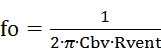
其中聲阻Rvent為Rs、Rg及Rv的和,即Rvent = Rs +Rg + Rv。The acoustic resistance Rvent is the sum of Rs, Rg and Rv, that is, Rvent = Rs + Rg + Rv.
圖4是根據本發明實施例示意性地示出所探討的靈敏度隨聲頻改變的圖式。參照圖4,截止頻率fo取決於聲阻Rvent。實線表示在具有小的聲阻Rvent值時靈敏度對聲頻(f)的回應,而虛線是在具有較大的聲阻Rvent時靈敏度對聲頻(f)的回應。Fig. 4 is a diagram schematically showing the sensitivity change with the audio frequency according to an embodiment of the present invention. Referring to Figure 4, the cutoff frequency fo depends on the acoustic resistance Rvent. The solid line represents the response of the sensitivity to the audio frequency (f) when the acoustic resistance Rvent is small, and the dashed line is the response of the sensitivity to the audio frequency (f) when the acoustic resistance Rvent is large.
在探討聲阻Rvent時,可在不對製作過程進行有效改變的條件下對Rs及Rv的電阻進行設定。聲阻Rg可為要被有效調節以顯著增大聲阻Rvent且因而降低截止頻率fo的因素。When discussing the acoustic resistance Rvent, the resistance of Rs and Rv can be set without effectively changing the manufacturing process. The acoustic resistance Rg may be a factor to be effectively adjusted to significantly increase the acoustic resistance Rvent and thus reduce the cut-off frequency fo.
如對圖1中的結構進行探討,儘管間隙d可被設計成具有足夠的間隙來增大聲阻Rvent,但是介電層102的介電材料在製作過程中不容易被刻蝕。As discussed in the structure in FIG. 1, although the gap d can be designed to have a sufficient gap to increase the acoustic resistance Rvent, the dielectric material of the
總的來說,狹縫106用於釋放膜片中的殘餘應力並調節膜片的剛度。狹縫106還用作用於平衡空氣壓力的附加排氣孔。然而,膜片中的狹縫106會形成低頻衰減。為了減小低頻衰減,排氣孔112與狹縫106之間的間隙d必須足夠長以形成高的聲阻。然而,長的間隙d將使從介電層102釋放膜片的MEMS釋放時間變長。如果MEMS釋放時間過長,則保護層108或電極板110(例如金屬焊盤)可能會被刻蝕劑損壞。In general, the
在本發明的實施例中,MEMS麥克風可在狹縫與排氣孔之間具有足夠的間隙d,且也可以快的速率刻蝕介電材料以避免至少對電極板的損壞。In the embodiment of the present invention, the MEMS microphone can have a sufficient gap d between the slit and the exhaust hole, and can also etch the dielectric material at a fast rate to avoid at least damage to the electrode plate.
圖5是根據本發明實施例示意性地示出MEMS麥克風的膜片的一部分的平面圖的圖式。參照圖5以及圖1中的類似部件,在實施例中,圖1中的膜片104被修改成膜片250。膜片250也可具有嵌置部50,嵌置部50被預先確定成嵌置在介電層102中以固持膜片250。膜片250的暴露部52暴露在介電層102的開口116中。膜片250的暴露部52在實施例中具有接合周邊區200、緩衝周邊區202及中心區204。接合周邊區200具有彈性結構,彈性結構具有狹縫106,緩衝周邊區202包括多個孔150且設置在接合周邊區200與中心區204之間。背板的保護層108的排氣孔112由膜片250之上的虛線區表示。FIG. 5 is a diagram schematically showing a plan view of a part of a diaphragm of a MEMS microphone according to an embodiment of the present invention. Referring to FIG. 5 and similar components in FIG. 1, in the embodiment, the
一般來說,排氣孔112與狹縫106之間的間隙d足夠長以增大聲阻。此外,為了保持膜片250從介電層102的快的釋放時間,在狹縫106與排氣孔112之間在緩衝周邊區202中形成有小的孔150。在對介電材料進行的刻蝕製程期間,刻蝕劑可經過孔150以對背板的保護層108與膜片250之間的介電材料進行刻蝕。另外,孔150可由小的孔構成,以使得聲阻Rvent也可甚至保持為高的。Generally, the gap d between the
圖6是根據本發明實施例示意性地示出沿圖5中的線I-II切割的MEMS麥克風的剖視圖的圖式。參照圖6,剖視圖是在與孔150及排氣孔112交叉的線I-II處切割的。緩衝周邊區202在內側處鄰接接合周邊區200。狹縫106分佈在接合周邊區200中且多個大小為小的孔150分佈在緩衝周邊區202中並環繞圖5中的中心區204。另一方面,圖5中的平面圖是在膜片250的平面上的剖視圖。狹縫106的寬度大於孔150的寬度。FIG. 6 is a diagram schematically showing a cross-sectional view of the MEMS microphone cut along the line I-II in FIG. 5 according to an embodiment of the present invention. Referring to FIG. 6, the cross-sectional view is cut at the line I-II intersecting the
圖7是根據本發明實施例示意性地示出沿圖5中的線II-III切割的MEMS麥克風的剖視圖的圖式。參照圖7,剖視圖是在不與孔150及排氣孔112交叉的線II-III處切割的。在此結構中,僅看到狹縫106。然而,實施例中的狹縫106及孔150的圖案並不會限制本發明。在實施例中,狹縫106可均勻地分佈。同樣,孔150也可均勻地分佈成環繞圖5中的中心區204的環。如也將更詳細地闡述,在實施例中,還可對孔150的密度進行調節以使刻蝕介電層102的速率更快。FIG. 7 is a diagram schematically showing a cross-sectional view of the MEMS microphone cut along the line II-III in FIG. 5 according to an embodiment of the present invention. Referring to FIG. 7, the cross-sectional view is cut at the line II-III that does not intersect the
圖8是根據本發明實施例示意性地示出具有孔的膜片的一部分的透視及剖視圖的圖式。參照圖8,孔150的大小可保持為小的以維持高的聲阻。孔150的寬度在實施例中可介於1微米到3微米之間的範圍內。在實施例中,孔150的形狀可為圓孔,此時寬度則是直徑,即半徑的兩倍2r。孔的聲阻與h/r4成比例,h是膜片250的厚度,也就是說,另一方面是膜片104的厚度。Fig. 8 is a diagram schematically showing a perspective and a cross-sectional view of a part of a diaphragm having a hole according to an embodiment of the present invention. Referring to FIG. 8, the size of the
圖9是根據本發明實施例示意性地示出製作流程中的MEMS麥克風的剖視圖的圖式。參照圖9且還部分地參照前面圖式中具有相同參考編號的元件,在製作方法方面,可形成初步結構。初步結構包括由矽形成的基板100,在基板100中具有開口114。在基板100上設置介電層102,介電層102具有被開口114暴露出的一部分,其中在介電層102中形成有膜片250。膜片250被配置成具有環繞開口114的嵌置部50及與開口114對應的位於嵌置部50內的暴露部52。暴露部52具有接合周邊區200、緩衝周邊區202及中心區204。接合周邊區200具有彈性結構,彈性結構具有狹縫106,緩衝周邊區包括多個孔150且設置在接合周邊區200與中心區204之間。在介電層102上設置具有保護層108及電極板110的背板252,其中背板252具有分佈在與膜片250的中心區204對應的區254處的排氣孔112。FIG. 9 is a diagram schematically showing a cross-sectional view of a MEMS microphone in a manufacturing process according to an embodiment of the present invention. Referring to FIG. 9 and also partially referring to the elements with the same reference numbers in the previous drawings, in terms of the manufacturing method, a preliminary structure can be formed. The preliminary structure includes a
如上所述,初步結構中的膜片250完全嵌置在介電層102中。As described above, the
圖10是根據本發明實施例示意性地示出製作流程中的MEMS麥克風的剖視圖的圖式。參照圖10,執行等向刻蝕製程220以通過基板的開口114及背板的排氣孔刻蝕介電層102,以在介電層102中形成開口116,從而暴露出膜片250的暴露部及背板252。膜片250的孔150及狹縫106允許刻蝕劑流過以對介電層102的介電材料進行刻蝕。Fig. 10 is a diagram schematically showing a cross-sectional view of a MEMS microphone in a manufacturing process according to an embodiment of the present invention. 10, an
如上所述,孔150確實在狹縫106與排氣孔112之間的部分處提供對介電層102的附加刻蝕能力。由於孔150,釋放膜片250的時間被有效地縮短。As described above, the
圖11是根據本發明實施例示意性地示出MEMS麥克風的俯視圖的圖式。參照圖11,如從MEMS麥克風的頂部以透視圖觀察,在實施例中,膜片250是圓盤。如上所述,圖11中示出具有排氣孔112的背板的僅一部分。然而,彈簧結構160作為具有狹縫106的彈性結構被更詳細地示出。彈簧結構160可以各種方式形成。在所述實施例中,狹縫106簡單地形成為直的並延伸成規則的圓環。然而,彈簧160的幾何形狀並不僅限於所述實施例。FIG. 11 is a diagram schematically showing a top view of a MEMS microphone according to an embodiment of the present invention. Referring to FIG. 11, as viewed in a perspective view from the top of the MEMS microphone, in an embodiment, the
圖12是根據本發明實施例示意性地示出MEMS麥克風的俯視圖的圖式。參照圖12,對於彈簧結構160,根據彈簧結構160的彎曲方式而定,狹縫106可為彎曲形狀。Fig. 12 is a diagram schematically showing a top view of a MEMS microphone according to an embodiment of the present invention. Referring to FIG. 12, for the
圖13是根據本發明實施例示意性地示出MEMS麥克風的俯視圖的圖式。參照圖13,在彈簧結構160的又一實施例中,彈簧結構可為曲折結構(meander structure),因此狹縫106具有分支。FIG. 13 is a diagram schematically showing a top view of a MEMS microphone according to an embodiment of the present invention. Referring to FIG. 13, in another embodiment of the
如上所述,在實際設計時,狹縫106取決於彈簧結構160。本發明中的彈簧結構並不僅限於所述實施例。As described above, in actual design, the
綜上所述,在實施例中,本發明提供一種微機電系統麥克風的結構,所述結構包括半導體的基板,在所述基板中具有第一開口。介電層設置在所述基板上,所述介電層具有與所述第一開口對應的第二開口。膜片位於所述第二開口內,具有由所述介電層固持的嵌置部及被所述第二開口暴露出的暴露部。所述暴露部具有接合周邊區、緩衝周邊區及中心區。所述接合周邊區具有彈性結構,所述彈性結構具有狹縫,所述緩衝周邊區包括多個孔且設置在所述接合周邊區與所述中心區之間。背板在所述第二開口上方設置在所述介電層上,其中所述背板包括分佈在與所述膜片的所述中心區對應的區處的排氣孔。In summary, in the embodiments, the present invention provides a structure of a MEMS microphone. The structure includes a semiconductor substrate, and the substrate has a first opening. The dielectric layer is disposed on the substrate, and the dielectric layer has a second opening corresponding to the first opening. The diaphragm is located in the second opening, and has an embedded portion held by the dielectric layer and an exposed portion exposed by the second opening. The exposed portion has a joining peripheral area, a buffer peripheral area, and a central area. The joint peripheral area has an elastic structure, the elastic structure has a slit, and the buffer peripheral area includes a plurality of holes and is disposed between the joint peripheral area and the central area. A back plate is disposed on the dielectric layer above the second opening, wherein the back plate includes exhaust holes distributed at a region corresponding to the central region of the diaphragm.
在實施例中,關於微機電系統麥克風的結構,所述背板包括:保護層,設置在所述介電層上;以及電極板,設置在所述保護層上。In an embodiment, regarding the structure of the MEMS microphone, the backplane includes: a protective layer disposed on the dielectric layer; and an electrode plate disposed on the protective layer.
在實施例中,關於微機電系統麥克風的結構,所述電極板位於所述保護層的面對所述膜片的一側上。In an embodiment, regarding the structure of the MEMS microphone, the electrode plate is located on the side of the protective layer facing the diaphragm.
在實施例中,關於微機電系統麥克風的結構,所述膜片的所述接合周邊區包括彈簧結構,其中所述狹縫形成在彈簧條之間。In an embodiment, regarding the structure of the MEMS microphone, the joint peripheral area of the diaphragm includes a spring structure, wherein the slit is formed between the spring bars.
在實施例中,關於微機電系統麥克風的結構,位於所述緩衝周邊區處的所述膜片的所述孔均勻地分佈在所述緩衝周邊區中。In an embodiment, regarding the structure of the MEMS microphone, the holes of the diaphragm located at the buffer peripheral area are evenly distributed in the buffer peripheral area.
在實施例中,關於微機電系統麥克風的結構,所述孔的寬度小於所述狹縫的寬度。In an embodiment, regarding the structure of the MEMS microphone, the width of the hole is smaller than the width of the slit.
在實施例中,關於微機電系統麥克風的結構,所述孔的所述寬度介於1微米與3微米之間。In an embodiment, regarding the structure of the MEMS microphone, the width of the hole is between 1 micrometer and 3 micrometers.
在實施例中,關於微機電系統麥克風的結構,所述膜片的所述緩衝周邊區在狹縫與所述排氣孔之間提供空間間隙以減小由所述狹縫引起的低頻衰減。In an embodiment, regarding the structure of the MEMS microphone, the buffer peripheral area of the diaphragm provides a space gap between the slit and the exhaust hole to reduce the low frequency attenuation caused by the slit.
在實施例中,關於微機電系統麥克風的結構,所述緩衝周邊區中的所述孔允許介電質刻蝕劑流過。In an embodiment, regarding the structure of the MEMS microphone, the hole in the buffer peripheral region allows the dielectric etchant to flow through.
在實施例中,關於微機電系統麥克風的結構,所述背板的所述排氣孔被分佈成環繞所述膜片的中心點的多個環。In an embodiment, regarding the structure of the MEMS microphone, the exhaust holes of the back plate are distributed into a plurality of rings surrounding the center point of the diaphragm.
在實施例中,本發明還提供一種製作微機電系統麥克風的方法。所述方法包括提供初步結構。所述初步結構包括矽基板,在所述矽基板中具有第一開口。介電層設置在所述矽基板上,具有被所述第一開口暴露出的一部分,其中在所述介電層中形成膜片。所述膜片被配置成具有環繞所述第一開口的嵌置部及與所述第一開口對應的位於所述嵌置部內的暴露部。所述暴露部具有接合周邊區、緩衝周邊區及中心區。所述接合周邊區具有彈性結構,所述彈性結構具有狹縫,所述緩衝周邊區包括多個孔且設置在所述接合周邊區與所述中心區之間。背板設置在所述介電層上,其中所述背板包括分佈在與所述膜片的所述中心區對應的區處的排氣孔。執行等向刻蝕製程,以穿過所述矽基板的所述第一開口及所述背板的所述排氣孔刻蝕所述介電層,以在所述介電層中形成第二開口,從而暴露出所述膜片的所述暴露部及所述背板。所述膜片的所述孔及所述狹縫允許刻蝕劑流過以對所述介電層的介電材料進行刻蝕。In an embodiment, the present invention also provides a method for manufacturing a microelectromechanical system microphone. The method includes providing a preliminary structure. The preliminary structure includes a silicon substrate with a first opening in the silicon substrate. The dielectric layer is disposed on the silicon substrate and has a part exposed by the first opening, wherein a diaphragm is formed in the dielectric layer. The diaphragm is configured to have an embedded portion surrounding the first opening and an exposed portion located in the embedded portion corresponding to the first opening. The exposed portion has a joining peripheral area, a buffer peripheral area, and a central area. The joint peripheral area has an elastic structure, the elastic structure has a slit, and the buffer peripheral area includes a plurality of holes and is disposed between the joint peripheral area and the central area. The back plate is disposed on the dielectric layer, wherein the back plate includes exhaust holes distributed at a region corresponding to the central region of the diaphragm. Perform an isotropic etching process to etch the dielectric layer through the first opening of the silicon substrate and the vent hole of the back plate to form a second in the dielectric layer Opening, thereby exposing the exposed portion of the diaphragm and the back plate. The hole and the slit of the diaphragm allow an etchant to flow through to etch the dielectric material of the dielectric layer.
在實施例中,關於所述製作微機電系統麥克風的方法,所述背板包括:保護層,設置在所述介電層上;以及電極板,設置在所述保護層上。In an embodiment, regarding the method of manufacturing a MEMS microphone, the backplane includes: a protective layer disposed on the dielectric layer; and an electrode plate disposed on the protective layer.
在實施例中,關於所述製作微機電系統麥克風的方法,所述電極板位於所述保護層的面對所述膜片的一側上。In an embodiment, regarding the method of manufacturing a MEMS microphone, the electrode plate is located on the side of the protective layer facing the diaphragm.
在實施例中,關於所述製作微機電系統麥克風的方法,所述膜片的所述接合周邊區包括彈簧結構,其中所述狹縫形成在彈簧條之間。In an embodiment, regarding the method of manufacturing a MEMS microphone, the joint peripheral area of the diaphragm includes a spring structure, wherein the slit is formed between the spring bars.
在實施例中,關於所述製作微機電系統麥克風的方法,位於所述緩衝周邊區處的所述膜片的所述孔均勻地分佈在所述緩衝周邊區中。In an embodiment, regarding the method of manufacturing a microelectromechanical system microphone, the holes of the diaphragm located at the buffer peripheral area are evenly distributed in the buffer peripheral area.
在實施例中,關於所述製作微機電系統麥克風的方法,所述孔的寬度小於所述狹縫的寬度。In an embodiment, regarding the method of manufacturing a microelectromechanical system microphone, the width of the hole is smaller than the width of the slit.
在實施例中,關於所述製作微機電系統麥克風的方法,所述孔的所述寬度介於1微米與3微米之間。In an embodiment, regarding the method of manufacturing a MEMS microphone, the width of the hole is between 1 micrometer and 3 micrometers.
在實施例中,關於所述製作微機電系統麥克風的方法,所述膜片的所述緩衝周邊區在狹縫與所述排氣孔之間提供空間間隙以減小由所述狹縫引起的低頻衰減。In an embodiment, with regard to the method of manufacturing a MEMS microphone, the buffer peripheral area of the diaphragm provides a space gap between the slit and the exhaust hole to reduce the amount caused by the slit Low frequency attenuation.
在實施例中,關於所述製作微機電系統麥克風的方法,所述緩衝周邊區中的所述孔增加對設置在所述緩衝周邊區處的所述介電材料的刻蝕能力。In an embodiment, regarding the method of manufacturing a microelectromechanical system microphone, the holes in the buffer peripheral area increase the etching ability of the dielectric material disposed at the buffer peripheral area.
在實施例中,關於所述製作微機電系統麥克風的方法,所述背板的所述排氣孔被分佈成環繞所述膜片的中心點的多個環。In an embodiment, regarding the method of manufacturing a MEMS microphone, the exhaust holes of the back plate are distributed into a plurality of rings surrounding the center point of the diaphragm.
在實施例中,提供膜片以在緩衝周邊區處形成多個孔。釋放膜片的時間有效地縮短。緩衝周邊區處的小的孔還可引起高的聲阻,從而降低靈敏度的低頻衰減。In an embodiment, the diaphragm is provided to form a plurality of holes at the buffer peripheral area. The time to release the diaphragm is effectively shortened. The small holes in the peripheral area of the buffer can also cause high acoustic resistance, thereby reducing the low-frequency attenuation of sensitivity.
雖然本發明已以實施例揭露如上,然其並非用以限定本發明,任何所屬技術領域中具有通常知識者,在不脫離本發明的精神和範圍內,當可作些許的更動與潤飾,故本發明的保護範圍當視後附的申請專利範圍所界定者為準。Although the present invention has been disclosed in the above embodiments, it is not intended to limit the present invention. Anyone with ordinary knowledge in the relevant technical field can make some changes and modifications without departing from the spirit and scope of the present invention. The protection scope of the present invention shall be subject to those defined by the attached patent application scope.
10:橫向擴散金屬氧化物半導體元件
50:嵌置部
52:暴露部
54、200:接合周邊區
100:矽基板/基板
102:介電層
104、250:膜片
106:狹縫
108:保護層
110:電極板
112:排氣孔
114、116:開口
122:MEMS麥克風
150:孔
160:彈簧結構/彈簧
202:緩衝周邊區
204:中心區
220:等向刻蝕製程
252:背板
254:區
d:間隙
fo:截止頻率10: Lateral diffusion metal oxide semiconductor components
50: Embedded part
52: exposed
圖1是根據本發明實施例示意性地示出所探討的MEMS麥克風的結構的剖視圖的圖式。 圖2是示意性地示出圖1中MEMS麥克風的膜片的一部分的平面圖的圖式。 圖3是根據本發明實施例示意性地示出所探討的MEMS麥克風中的感測問題的圖式。 圖4是根據本發明實施例示意性地示出所探討的靈敏度隨聲頻改變的圖式。 圖5是根據本發明實施例示意性地示出MEMS麥克風的膜片的一部分的平面圖的圖式。 圖6是根據本發明實施例示意性地示出沿圖5中的線I-II切割的MEMS麥克風的剖視圖的圖式。 圖7是根據本發明實施例示意性地示出沿圖5中的線II-III切割的MEMS麥克風的剖視圖的圖式。 圖8是根據本發明實施例示意性地示出具有孔的膜片的一部分的透視及剖視圖的圖式。 圖9是根據本發明實施例示意性地示出製作流程中的MEMS麥克風的剖視圖的圖式。 圖10是根據本發明實施例示意性地示出製作流程中的MEMS麥克風的剖視圖的圖式。 圖11是根據本發明實施例示意性地示出MEMS麥克風的俯視圖的圖式。 圖12是根據本發明實施例示意性地示出MEMS麥克風的俯視圖的圖式。 圖13是根據本發明實施例示意性地示出MEMS麥克風的俯視圖的圖式。FIG. 1 is a diagram schematically showing a cross-sectional view of the structure of a MEMS microphone under discussion according to an embodiment of the present invention. FIG. 2 is a diagram schematically showing a plan view of a part of a diaphragm of the MEMS microphone in FIG. 1. FIG. 3 is a diagram schematically showing the sensing problem in the MEMS microphone under discussion according to an embodiment of the present invention. Fig. 4 is a diagram schematically showing the sensitivity change with the audio frequency according to an embodiment of the present invention. FIG. 5 is a diagram schematically showing a plan view of a part of a diaphragm of a MEMS microphone according to an embodiment of the present invention. FIG. 6 is a diagram schematically showing a cross-sectional view of the MEMS microphone cut along the line I-II in FIG. 5 according to an embodiment of the present invention. FIG. 7 is a diagram schematically showing a cross-sectional view of the MEMS microphone cut along the line II-III in FIG. 5 according to an embodiment of the present invention. Fig. 8 is a diagram schematically showing a perspective and a cross-sectional view of a part of a diaphragm having a hole according to an embodiment of the present invention. FIG. 9 is a diagram schematically showing a cross-sectional view of a MEMS microphone in a manufacturing process according to an embodiment of the present invention. Fig. 10 is a diagram schematically showing a cross-sectional view of a MEMS microphone in a manufacturing process according to an embodiment of the present invention. FIG. 11 is a diagram schematically showing a top view of a MEMS microphone according to an embodiment of the present invention. Fig. 12 is a diagram schematically showing a top view of a MEMS microphone according to an embodiment of the present invention. FIG. 13 is a diagram schematically showing a top view of a MEMS microphone according to an embodiment of the present invention.
50:嵌置部50: Embedded part
52:暴露部52: exposed part
106:狹縫106: slit
112:排氣孔112: Vent
150:孔150: hole
200:接合周邊區200: Join the surrounding area
202:緩衝周邊區202: Buffer the surrounding area
204:中心區204: Central Area
250:膜片250: diaphragm
Claims (20)
Applications Claiming Priority (2)
| Application Number | Priority Date | Filing Date | Title |
|---|---|---|---|
| US16/673,962 | 2019-11-05 | ||
| US16/673,962 US11172287B2 (en) | 2019-11-05 | 2019-11-05 | Structure of micro-electro-mechanical-system microphone and method for fabricating the same |
Publications (2)
| Publication Number | Publication Date |
|---|---|
| TW202119829A true TW202119829A (en) | 2021-05-16 |
| TWI751451B TWI751451B (en) | 2022-01-01 |
Family
ID=75688426
Family Applications (1)
| Application Number | Title | Priority Date | Filing Date |
|---|---|---|---|
| TW108141763A TWI751451B (en) | 2019-11-05 | 2019-11-18 | Structure of micro-electro-mechanical-system microphone and method for fabricating the same |
Country Status (3)
| Country | Link |
|---|---|
| US (1) | US11172287B2 (en) |
| CN (1) | CN112788508B (en) |
| TW (1) | TWI751451B (en) |
Families Citing this family (17)
| Publication number | Priority date | Publication date | Assignee | Title |
|---|---|---|---|---|
| DE102020108527B4 (en) | 2020-03-27 | 2021-12-09 | Tdk Corporation | MICROPHONE COMPONENT AND METHOD FOR MANUFACTURING A MICROPHONE COMPONENT |
| US11716576B2 (en) * | 2021-02-19 | 2023-08-01 | Skyworks Solutions, Inc. | Dummy electrodes for performance improvement of piezoelectric microelectromechanical system microphones |
| US12358782B2 (en) | 2021-02-19 | 2025-07-15 | Skyworks Solutions, Inc. | Piezoelectric microelectromechanical system microphone sensitivity improvement by anchor engineering |
| US12351450B2 (en) | 2021-04-19 | 2025-07-08 | Skyworks Solutions, Inc. | Dual membrane piezoelectric microelectromechanical system microphone |
| US11979712B2 (en) | 2021-07-01 | 2024-05-07 | Skyworks Solutions, Inc. | Extension structures in piezoelectric microelectromechanical system microphones |
| US12570520B2 (en) | 2021-07-09 | 2026-03-10 | Skyworks Solutions, Inc. | Cantilevered piezoelectric microelectromechanical systems microphone with stress compensation |
| US12212925B2 (en) | 2021-08-04 | 2025-01-28 | Skyworks Global Pte. Ltd. | Piezoelectric microelectromechanical system corrugated microphone |
| US12101601B2 (en) | 2021-09-07 | 2024-09-24 | Skyworks Solutions, Inc. | Piezoelectric microelectromechanical system microphone with optimized output capacitance |
| US12513470B2 (en) | 2021-10-05 | 2025-12-30 | Skyworks Solutions, Inc. | Piezoelectric MEMS microphone with spring region |
| US12328562B2 (en) | 2021-10-06 | 2025-06-10 | Skyworks Solutions, Inc. | Anchor silicon dioxide layer for piezoelectric microelectromechanical system microphone |
| US12413914B2 (en) * | 2021-10-27 | 2025-09-09 | Skyworks Global Pte. Ltd. | Piezoelectric microelectromechanical system microphone with compliant anchors |
| CN216852339U (en) * | 2021-12-31 | 2022-06-28 | 瑞声声学科技(深圳)有限公司 | A MEMS microphone |
| US12495260B2 (en) | 2022-01-25 | 2025-12-09 | Skyworks Solutions, Inc. | Method of making mems microphone with an anchor |
| US12323753B2 (en) * | 2022-03-31 | 2025-06-03 | Fortemedia, Inc. | Micro-electro-mechanical system structure |
| US20230339742A1 (en) * | 2022-04-22 | 2023-10-26 | Fortemedia, Inc. | Mems structure |
| CN217693708U (en) * | 2022-07-01 | 2022-10-28 | 瑞声声学科技(深圳)有限公司 | MEMS microphone |
| US12507014B2 (en) * | 2023-06-07 | 2025-12-23 | Aac Acoustic Technologies (Shenzhen) Co., Ltd. | Diaphragm and MEMS microphone |
Family Cites Families (7)
| Publication number | Priority date | Publication date | Assignee | Title |
|---|---|---|---|---|
| CN103281661B (en) | 2013-05-09 | 2019-02-05 | 上海集成电路研发中心有限公司 | A kind of MEMS microphone structure and its manufacturing method |
| CN105721997B (en) | 2015-04-08 | 2019-04-05 | 华景科技无锡有限公司 | A kind of MEMS silicon microphone and preparation method thereof |
| US10250998B2 (en) * | 2016-10-26 | 2019-04-02 | Solid State Systems Co., Ltd. | Micro-electro-mechanical systems (MEMS) device and method for fabricating the MEMS |
| KR102212575B1 (en) * | 2017-02-02 | 2021-02-04 | 현대자동차 주식회사 | Microphone and manufacturing method thereof |
| US10343898B1 (en) * | 2018-01-08 | 2019-07-09 | Fortemedia, Inc. | MEMS microphone with tunable sensitivity |
| US10390145B1 (en) | 2018-04-02 | 2019-08-20 | Solid State System Co., Ltd. | Micro electro mechanical system (MEMS) microphone |
| US11459230B2 (en) * | 2019-04-23 | 2022-10-04 | Fortemedia, Inc. | MEMS microphone |
-
2019
- 2019-11-05 US US16/673,962 patent/US11172287B2/en active Active
- 2019-11-18 TW TW108141763A patent/TWI751451B/en active
- 2019-12-10 CN CN201911256372.XA patent/CN112788508B/en active Active
Also Published As
| Publication number | Publication date |
|---|---|
| US20210136483A1 (en) | 2021-05-06 |
| TWI751451B (en) | 2022-01-01 |
| CN112788508A (en) | 2021-05-11 |
| US11172287B2 (en) | 2021-11-09 |
| CN112788508B (en) | 2022-09-13 |
Similar Documents
| Publication | Publication Date | Title |
|---|---|---|
| TWI751451B (en) | Structure of micro-electro-mechanical-system microphone and method for fabricating the same | |
| CN101828409B (en) | Silicon microphone with enhanced impact test structure using bonding wires | |
| EP2387255B1 (en) | Acoustic sensor and microphone | |
| JP5422189B2 (en) | Sensing membrane | |
| CN109729483B (en) | Integrated microphone unit | |
| US20080175418A1 (en) | Microphone with Pressure Relief | |
| US9641939B2 (en) | Acoustic transducer and microphone | |
| CN103688556A (en) | Components with micromechanical microphone structures | |
| WO2018094963A1 (en) | Micro-silicon microphone and manufacturing method thereof | |
| CN105492373A (en) | Silicon microphone with high aspect ratio corrugated diaphragm and package having same | |
| US11496820B2 (en) | MEMS device with quadrilateral trench and insert | |
| CN107005772A (en) | Form the integration packaging and manufacture method of wide sensing gap MEMS condenser microphone | |
| JP2008099212A (en) | Capacitor microphone and its manufacturing method | |
| CN212435925U (en) | MEMS microphone and its microelectromechanical structure | |
| CN114697841A (en) | MEMS microphone and vibrating diaphragm structure thereof | |
| KR102322258B1 (en) | Microphone and manufacturing method thereof | |
| CN106608614B (en) | Method for manufacturing MEMS structure | |
| WO2022007000A1 (en) | Mems microphone | |
| JP6307171B2 (en) | MEMS microphone | |
| TW202119830A (en) | Structure of micro-electro-mechanical-system microphone | |
| CN114079844B (en) | MEMS microphone and its micro-electromechanical structure | |
| CN215072978U (en) | Microphone chip, MEMS microphone and electronic equipment | |
| KR20140122848A (en) | Mems microphone having piezo membrane | |
| JP2010109416A (en) | Pressure transducer and method of manufacturing the same | |
| KR101610128B1 (en) | Micro phone and method manufacturing the same |