TW202127635A - Time of flight sensing system and image sensor used therein - Google Patents
Time of flight sensing system and image sensor used therein Download PDFInfo
- Publication number
- TW202127635A TW202127635A TW109124423A TW109124423A TW202127635A TW 202127635 A TW202127635 A TW 202127635A TW 109124423 A TW109124423 A TW 109124423A TW 109124423 A TW109124423 A TW 109124423A TW 202127635 A TW202127635 A TW 202127635A
- Authority
- TW
- Taiwan
- Prior art keywords
- pixel
- signal
- control signal
- rows
- image sensor
- Prior art date
Links
Images


Classifications
-
- H—ELECTRICITY
- H04—ELECTRIC COMMUNICATION TECHNIQUE
- H04N—PICTORIAL COMMUNICATION, e.g. TELEVISION
- H04N25/00—Circuitry of solid-state image sensors [SSIS]; Control thereof
- H04N25/70—SSIS architectures; Circuits associated therewith
- H04N25/703—SSIS architectures incorporating pixels for producing signals other than image signals
- H04N25/705—Pixels for depth measurement, e.g. RGBZ
-
- G—PHYSICS
- G01—MEASURING; TESTING
- G01S—RADIO DIRECTION-FINDING; RADIO NAVIGATION; DETERMINING DISTANCE OR VELOCITY BY USE OF RADIO WAVES; LOCATING OR PRESENCE-DETECTING BY USE OF THE REFLECTION OR RERADIATION OF RADIO WAVES; ANALOGOUS ARRANGEMENTS USING OTHER WAVES
- G01S17/00—Systems using the reflection or reradiation of electromagnetic waves other than radio waves, e.g. lidar systems
- G01S17/02—Systems using the reflection of electromagnetic waves other than radio waves
- G01S17/06—Systems determining position data of a target
- G01S17/08—Systems determining position data of a target for measuring distance only
- G01S17/10—Systems determining position data of a target for measuring distance only using transmission of interrupted, pulse-modulated waves
-
- G—PHYSICS
- G01—MEASURING; TESTING
- G01S—RADIO DIRECTION-FINDING; RADIO NAVIGATION; DETERMINING DISTANCE OR VELOCITY BY USE OF RADIO WAVES; LOCATING OR PRESENCE-DETECTING BY USE OF THE REFLECTION OR RERADIATION OF RADIO WAVES; ANALOGOUS ARRANGEMENTS USING OTHER WAVES
- G01S17/00—Systems using the reflection or reradiation of electromagnetic waves other than radio waves, e.g. lidar systems
- G01S17/02—Systems using the reflection of electromagnetic waves other than radio waves
- G01S17/06—Systems determining position data of a target
- G01S17/08—Systems determining position data of a target for measuring distance only
- G01S17/32—Systems determining position data of a target for measuring distance only using transmission of continuous waves, whether amplitude-, frequency-, or phase-modulated, or unmodulated
- G01S17/36—Systems determining position data of a target for measuring distance only using transmission of continuous waves, whether amplitude-, frequency-, or phase-modulated, or unmodulated with phase comparison between the received signal and the contemporaneously transmitted signal
-
- G—PHYSICS
- G01—MEASURING; TESTING
- G01S—RADIO DIRECTION-FINDING; RADIO NAVIGATION; DETERMINING DISTANCE OR VELOCITY BY USE OF RADIO WAVES; LOCATING OR PRESENCE-DETECTING BY USE OF THE REFLECTION OR RERADIATION OF RADIO WAVES; ANALOGOUS ARRANGEMENTS USING OTHER WAVES
- G01S17/00—Systems using the reflection or reradiation of electromagnetic waves other than radio waves, e.g. lidar systems
- G01S17/88—Lidar systems specially adapted for specific applications
- G01S17/89—Lidar systems specially adapted for specific applications for mapping or imaging
- G01S17/894—Three-dimensional [3D] imaging with simultaneous measurement of time-of-flight at a two-dimensional [2D] array of receiver pixels, e.g. time-of-flight cameras or flash lidar
-
- G—PHYSICS
- G01—MEASURING; TESTING
- G01S—RADIO DIRECTION-FINDING; RADIO NAVIGATION; DETERMINING DISTANCE OR VELOCITY BY USE OF RADIO WAVES; LOCATING OR PRESENCE-DETECTING BY USE OF THE REFLECTION OR RERADIATION OF RADIO WAVES; ANALOGOUS ARRANGEMENTS USING OTHER WAVES
- G01S7/00—Details of systems according to groups G01S13/00, G01S15/00, G01S17/00
- G01S7/48—Details of systems according to groups G01S13/00, G01S15/00, G01S17/00 of systems according to group G01S17/00
- G01S7/481—Constructional features, e.g. arrangements of optical elements
- G01S7/4816—Constructional features, e.g. arrangements of optical elements of receivers alone
-
- G—PHYSICS
- G01—MEASURING; TESTING
- G01S—RADIO DIRECTION-FINDING; RADIO NAVIGATION; DETERMINING DISTANCE OR VELOCITY BY USE OF RADIO WAVES; LOCATING OR PRESENCE-DETECTING BY USE OF THE REFLECTION OR RERADIATION OF RADIO WAVES; ANALOGOUS ARRANGEMENTS USING OTHER WAVES
- G01S7/00—Details of systems according to groups G01S13/00, G01S15/00, G01S17/00
- G01S7/48—Details of systems according to groups G01S13/00, G01S15/00, G01S17/00 of systems according to group G01S17/00
- G01S7/483—Details of pulse systems
- G01S7/486—Receivers
- G01S7/4861—Circuits for detection, sampling, integration or read-out
- G01S7/4863—Detector arrays, e.g. charge-transfer gates
-
- G—PHYSICS
- G01—MEASURING; TESTING
- G01S—RADIO DIRECTION-FINDING; RADIO NAVIGATION; DETERMINING DISTANCE OR VELOCITY BY USE OF RADIO WAVES; LOCATING OR PRESENCE-DETECTING BY USE OF THE REFLECTION OR RERADIATION OF RADIO WAVES; ANALOGOUS ARRANGEMENTS USING OTHER WAVES
- G01S7/00—Details of systems according to groups G01S13/00, G01S15/00, G01S17/00
- G01S7/48—Details of systems according to groups G01S13/00, G01S15/00, G01S17/00 of systems according to group G01S17/00
- G01S7/483—Details of pulse systems
- G01S7/486—Receivers
- G01S7/4865—Time delay measurement, e.g. time-of-flight measurement, time of arrival measurement or determining the exact position of a peak
-
- G—PHYSICS
- G01—MEASURING; TESTING
- G01S—RADIO DIRECTION-FINDING; RADIO NAVIGATION; DETERMINING DISTANCE OR VELOCITY BY USE OF RADIO WAVES; LOCATING OR PRESENCE-DETECTING BY USE OF THE REFLECTION OR RERADIATION OF RADIO WAVES; ANALOGOUS ARRANGEMENTS USING OTHER WAVES
- G01S7/00—Details of systems according to groups G01S13/00, G01S15/00, G01S17/00
- G01S7/48—Details of systems according to groups G01S13/00, G01S15/00, G01S17/00 of systems according to group G01S17/00
- G01S7/491—Details of non-pulse systems
- G01S7/4912—Receivers
- G01S7/4913—Circuits for detection, sampling, integration or read-out
- G01S7/4914—Circuits for detection, sampling, integration or read-out of detector arrays, e.g. charge-transfer gates
-
- H—ELECTRICITY
- H04—ELECTRIC COMMUNICATION TECHNIQUE
- H04N—PICTORIAL COMMUNICATION, e.g. TELEVISION
- H04N25/00—Circuitry of solid-state image sensors [SSIS]; Control thereof
- H04N25/50—Control of the SSIS exposure
- H04N25/57—Control of the dynamic range
- H04N25/59—Control of the dynamic range by controlling the amount of charge storable in the pixel, e.g. modification of the charge conversion ratio of the floating node capacitance
-
- H—ELECTRICITY
- H04—ELECTRIC COMMUNICATION TECHNIQUE
- H04N—PICTORIAL COMMUNICATION, e.g. TELEVISION
- H04N25/00—Circuitry of solid-state image sensors [SSIS]; Control thereof
- H04N25/60—Noise processing, e.g. detecting, correcting, reducing or removing noise
-
- H—ELECTRICITY
- H10—SEMICONDUCTOR DEVICES; ELECTRIC SOLID-STATE DEVICES NOT OTHERWISE PROVIDED FOR
- H10F—INORGANIC SEMICONDUCTOR DEVICES SENSITIVE TO INFRARED RADIATION, LIGHT, ELECTROMAGNETIC RADIATION OF SHORTER WAVELENGTH OR CORPUSCULAR RADIATION
- H10F39/00—Integrated devices, or assemblies of multiple devices, comprising at least one element covered by group H10F30/00, e.g. radiation detectors comprising photodiode arrays
- H10F39/10—Integrated devices
- H10F39/12—Image sensors
- H10F39/18—Complementary metal-oxide-semiconductor [CMOS] image sensors; Photodiode array image sensors
-
- H—ELECTRICITY
- H10—SEMICONDUCTOR DEVICES; ELECTRIC SOLID-STATE DEVICES NOT OTHERWISE PROVIDED FOR
- H10F—INORGANIC SEMICONDUCTOR DEVICES SENSITIVE TO INFRARED RADIATION, LIGHT, ELECTROMAGNETIC RADIATION OF SHORTER WAVELENGTH OR CORPUSCULAR RADIATION
- H10F39/00—Integrated devices, or assemblies of multiple devices, comprising at least one element covered by group H10F30/00, e.g. radiation detectors comprising photodiode arrays
- H10F39/80—Constructional details of image sensors
- H10F39/803—Pixels having integrated switching, control, storage or amplification elements
Landscapes
- Engineering & Computer Science (AREA)
- Physics & Mathematics (AREA)
- Computer Networks & Wireless Communication (AREA)
- General Physics & Mathematics (AREA)
- Radar, Positioning & Navigation (AREA)
- Remote Sensing (AREA)
- Electromagnetism (AREA)
- Multimedia (AREA)
- Signal Processing (AREA)
- Optical Radar Systems And Details Thereof (AREA)
- Transforming Light Signals Into Electric Signals (AREA)
- Photometry And Measurement Of Optical Pulse Characteristics (AREA)
Abstract
Description
本公開係關於使用飛行時間(TOF)系統的感測裝置,並且更具體地係關於用於提高感測裝置的解析度或精度的設備。The present disclosure relates to a sensing device using a time-of-flight (TOF) system, and more specifically to a device for improving the resolution or accuracy of the sensing device.
飛行時間(time-of-flight, TOF)系統測量光或信號從原點行進到物體並從物體反射回源所花費的時間,以計算距物體的距離,其中總往返行程時間表示飛行時間。原點可以是光或信號的源,諸如TOF系統的TOF相機。TOF相機基於物體與TOF相機之間的距離輸出包括物體的深度資訊的圖像。傳統相機能夠輸出表示物體的顏色和形狀的二維(2D)圖像,但是TOF相機可以輸出不僅表示物體的2D圖像而且還表示物體的深度的三維(3D)圖像。The time-of-flight (TOF) system measures the time it takes for light or signal to travel from the origin to the object and reflect from the object back to the source to calculate the distance to the object, where the total round trip time represents the time of flight. The origin can be a source of light or a signal, such as a TOF camera of a TOF system. The TOF camera outputs an image including depth information of the object based on the distance between the object and the TOF camera. A conventional camera can output a two-dimensional (2D) image that represents the color and shape of an object, but a TOF camera can output not only a 2D image of the object but also a three-dimensional (3D) image that represents the depth of the object.
相關申請的交叉引用Cross-references to related applications
本專利申請請求於2019年12月9日提交的韓國專利申請No. 10-2019-0162790的權益,其全部公開內容透過引用合併於此。This patent application requests the rights of Korean Patent Application No. 10-2019-0162790 filed on December 9, 2019, the entire disclosure of which is incorporated herein by reference.
本公開的實施方式可以提供一種被配置為避免從每個像素獲得的資訊的失真的設備。失真可能是由於飛行時間(time-of-flight, TOF)感測系統中採用的圖像感測器的像素陣列中包括的像素與配置為驅動像素陣列的驅動電路之間的距離差而發生的。The embodiments of the present disclosure can provide a device configured to avoid distortion of information obtained from each pixel. Distortion may occur due to the distance difference between the pixels included in the pixel array of the image sensor used in the time-of-flight (TOF) sensing system and the drive circuit configured to drive the pixel array .
此外,本公開的實施方式可以提供一種設備,該設備被配置為向飛行時間(TOF)感測系統中包括以多個列和多個行佈置的多個像素的像素陣列以能夠補償驅動電路與每個像素之間的距離差的順序提供驅動電壓。In addition, the embodiments of the present disclosure may provide an apparatus configured to add a pixel array including a plurality of pixels arranged in a plurality of columns and a plurality of rows to a time of flight (TOF) sensing system to be able to compensate the driving circuit and The driving voltage is provided in the order of the distance difference between each pixel.
另外,本公開的實施方式可以提供一種設備,該設備被配置為向佈置在像素陣列的每兩行中的多個像素提供驅動電壓,以補償像素之間由於在從驅動電路輸出的驅動電壓的傳送過程中所存在的延遲、電阻等引起的操作差異。隨著TOF感測系統中所包括的圖像感測器的尺寸增加,延遲、電阻等可以增加。驅動電壓可以為每個像素供電。驅動電路可以針對像素陣列的每兩行生成並提供驅動電壓。例如,向每個像素提供驅動電壓的驅動電路可以聯接至像素陣列的每兩行。In addition, the embodiments of the present disclosure may provide an apparatus configured to provide driving voltages to a plurality of pixels arranged in every two rows of a pixel array to compensate for the difference between the pixels due to the driving voltage output from the driving circuit. Operation differences caused by delays and resistances in the transmission process. As the size of the image sensor included in the TOF sensing system increases, delay, resistance, etc. may increase. The driving voltage can power each pixel. The driving circuit can generate and provide driving voltages for every two rows of the pixel array. For example, a driving circuit that provides a driving voltage to each pixel may be coupled to every two rows of the pixel array.
在實施方式中,在飛行時間(TOF)感測系統中所採用的圖像感測器可以包括像素陣列,其包括佈置成多個列和多個行的多個像素,每個像素回應於入射光而生成一定量的電荷;以及第一驅動電路,其被配置為經由多個行向每個像素提供驅動控制信號。第一驅動電路可以被配置為經由奇數行和偶數行中的一者來提供驅動控制信號。In an embodiment, the image sensor used in the time-of-flight (TOF) sensing system may include a pixel array including a plurality of pixels arranged in a plurality of columns and a plurality of rows, each pixel responding to the incident A certain amount of electric charge is generated by light; and a first driving circuit configured to provide a driving control signal to each pixel via a plurality of rows. The first driving circuit may be configured to provide a driving control signal via one of odd-numbered rows and even-numbered rows.
作為示例而非限制,圖像感測器可以具有第一結構或第二結構,在第一結構中第一驅動電路向奇數行的端子提供驅動控制信號,在第二結構中第一驅動電路向偶數行的端子提供驅動控制信號。奇數行的另一端子可以聯接至偶數行的另一端子。As an example and not limitation, the image sensor may have a first structure or a second structure. The terminals on the even-numbered rows provide drive control signals. The other terminal of the odd-numbered row may be connected to the other terminal of the even-numbered row.
圖像感測器可以進一步包括第二驅動電路,其被配置為經由奇數行和偶數行中的另一者來提供驅動控制信號。The image sensor may further include a second driving circuit configured to provide a driving control signal via the other of the odd-numbered rows and the even-numbered rows.
第一驅動電路和第二驅動電路可以位於像素陣列的相對兩側。The first driving circuit and the second driving circuit may be located on opposite sides of the pixel array.
像素陣列與第一驅動電路和第二驅動電路中的每個之間的距離可以相等。The distance between the pixel array and each of the first driving circuit and the second driving circuit may be equal.
每個像素可以包括至少一個光電二極體和至少一個轉移閘。每個像素可以具有相同數量的光電二極體和相同數量的轉移閘。驅動控制信號可以被輸入到至少一個轉移閘。Each pixel may include at least one photodiode and at least one transfer gate. Each pixel can have the same number of photodiodes and the same number of transfer gates. The drive control signal may be input to at least one transfer gate.
像素可以包括:第一接收電路,其被配置為在第一相位區段中接收入射光;以及第二接收電路,其被配置為在與第一相位區段相反的第二相位區段中接收入射光。The pixel may include: a first receiving circuit configured to receive incident light in a first phase section; and a second receiving circuit configured to receive incident light in a second phase section opposite to the first phase section Incident light.
在另一實施方式中,包括於飛行時間(TOF)感測系統中的圖像感測器可以包括:像素陣列,其包括佈置成多個列和多個行的多個像素,每個像素回應於入射光而生成一定量的電荷;第一驅動電路,其被配置為經由多個行中的一些行向一些像素提供第一驅動控制信號;以及第二驅動電路,其被配置為經由其餘行向其餘像素提供第二驅動控制信號。In another embodiment, the image sensor included in the time-of-flight (TOF) sensing system may include: a pixel array including a plurality of pixels arranged in a plurality of columns and a plurality of rows, each pixel responding A certain amount of electric charge is generated in response to incident light; a first driving circuit configured to provide a first driving control signal to some pixels through some rows of a plurality of rows; and a second driving circuit configured to pass through the remaining rows The second driving control signal is provided to the remaining pixels.
例如,當經由多個行中的奇數行傳送第一驅動控制信號時,可以經由多個行中的偶數行傳送第二驅動控制信號。在另一示例中,當經由多個行中的偶數行傳送第一驅動控制信號時,可以經由多個行中的奇數行傳送第二驅動控制信號。For example, when the first driving control signal is transmitted via odd-numbered rows among the plurality of rows, the second driving control signal may be transmitted via even-numbered rows among the plurality of rows. In another example, when the first driving control signal is transmitted through an even-numbered row among the plurality of rows, the second driving control signal may be transmitted through an odd-numbered row among the plurality of rows.
可以經由多個行中的交替行來分別提供第一驅動控制信號和第二驅動控制信號。The first driving control signal and the second driving control signal may be provided via alternate rows among the plurality of rows, respectively.
第一驅動電路和第二驅動電路可以佈置在像素陣列的相對兩側。The first driving circuit and the second driving circuit may be arranged on opposite sides of the pixel array.
每個像素可以包括至少一個光電二極體和至少一個轉移閘。每個像素可以包括相同數量的光電二極體和相同數量的轉移閘。驅動控制信號可以輸入至每個像素的至少一個轉移閘。Each pixel may include at least one photodiode and at least one transfer gate. Each pixel may include the same number of photodiodes and the same number of transfer gates. The drive control signal can be input to at least one transfer gate of each pixel.
圖像感測器可以還包括:信號轉換器,其被配置為將從像素陣列輸出的像素資訊轉換為數位信號。The image sensor may further include: a signal converter configured to convert pixel information output from the pixel array into a digital signal.
在另一實施方式中,飛行時間(TOF)感測系統可以包括:發射器,其被配置為輸出具有預設相位的調變信號;圖像感測器,其被配置為接收回應於從物體反射的調變信號而輸入的反射信號;以及信號處理器,其被配置為基於調變信號和反射信號之間的相位關係來確定距物體的距離。圖像感測器可以包括:像素陣列,其包括佈置成多個列和多個行的多個像素,每個像素回應於反射信號而生成一定量的電荷;以及第一驅動電路,其被配置為經由多個行向每個像素提供驅動控制信號。第一驅動電路可以被配置為經由奇數行和偶數行中的一者來提供驅動控制信號。In another embodiment, a time-of-flight (TOF) sensing system may include: a transmitter configured to output a modulation signal having a preset phase; an image sensor configured to receive a response to a slave object A reflected signal inputted by a reflected modulated signal; and a signal processor configured to determine the distance to the object based on the phase relationship between the modulated signal and the reflected signal. The image sensor may include: a pixel array including a plurality of pixels arranged in a plurality of columns and a plurality of rows, each pixel generating a certain amount of electric charge in response to a reflected signal; and a first driving circuit configured To provide drive control signals to each pixel via a plurality of rows. The first driving circuit may be configured to provide a driving control signal via one of odd-numbered rows and even-numbered rows.
圖像感測器可以具有第一結構或第二結構,在第一結構中第一驅動電路向奇數行的端子提供驅動控制信號,在第二結構中第一驅動電路向偶數行的端子提供驅動控制信號。奇數行的另一端子可以聯接至偶數行的另一端子。The image sensor may have a first structure or a second structure. In the first structure, the first drive circuit provides drive control signals to the terminals of the odd-numbered rows, and in the second structure, the first drive circuit provides drive to the terminals of the even-numbered rows. control signal. The other terminal of the odd-numbered row may be connected to the other terminal of the even-numbered row.
圖像感測器可以還包括:第二驅動電路,其被配置為經由奇數行和偶數行中的另一者來提供驅動控制信號。The image sensor may further include: a second driving circuit configured to provide a driving control signal via the other of the odd-numbered rows and the even-numbered rows.
第一驅動電路和第二驅動電路可以位於像素陣列的相對兩側。The first driving circuit and the second driving circuit may be located on opposite sides of the pixel array.
像素陣列與第一驅動電路和第二驅動電路中的每個之間的距離可以相等。The distance between the pixel array and each of the first driving circuit and the second driving circuit may be equal.
每個像素可以包括至少一個光電二極體和至少一個轉移閘。每個像素可以包括相同數量的光電二極體和相同數量的轉移閘。驅動控制信號可以輸入到每個像素的至少一個轉移閘。Each pixel may include at least one photodiode and at least one transfer gate. Each pixel may include the same number of photodiodes and the same number of transfer gates. The drive control signal can be input to at least one transfer gate of each pixel.
像素可以包括:第一接收電路,其被配置為在第一相位區段中接收入射光;以及第二接收電路,其被配置為在與第一相位區段相反的第二相位區段中接收入射光。The pixel may include: a first receiving circuit configured to receive incident light in a first phase section; and a second receiving circuit configured to receive incident light in a second phase section opposite to the first phase section Incident light.
在另一實施方式中,圖像感測器可以包括:像素陣列,其包括沿列線和行線佈置的像素,每個像素被配置為生成電荷,電荷的量對應於由相應像素感測到的入射光的量;以及驅動電路,其在像素陣列的外圍聯接至行線,並且被配置為透過每對奇數行線和偶數行線向像素提供與入射光具有基本上相同的週期的驅動控制信號,使得由佈置在成對列線上的兩個像素感測到的量之和基本相同。像素陣列可以被配置為生成由佈置在成對列線上的每對兩個像素生成的電荷之和。In another embodiment, the image sensor may include: a pixel array including pixels arranged along column lines and row lines, each pixel is configured to generate electric charge, the amount of electric charge corresponding to that sensed by the corresponding pixel The amount of incident light; and a drive circuit, which is coupled to the row lines at the periphery of the pixel array, and is configured to provide the pixels with drive control having substantially the same period as the incident light through each pair of odd and even row lines Signal such that the sum of the quantities sensed by the two pixels arranged on the pair of column lines is substantially the same. The pixel array may be configured to generate a sum of charges generated by each pair of two pixels arranged on a pair of column lines.
本公開包括對“一個實施方式”或“一實施方式”的引用。短語“在一個實施方式中”或“在一實施方式中”的出現並不一定是指相同的實施方式。特定特徵、結構或特性可以以與本公開一致的任何合適方式來組合。The present disclosure includes references to "one embodiment" or "an embodiment." The appearances of the phrase "in one embodiment" or "in an embodiment" do not necessarily refer to the same embodiment. Specific features, structures, or characteristics can be combined in any suitable manner consistent with the present disclosure.
下面參照附圖描述本公開的各種實施方式。然而,本公開的元件和特徵可以不同地配置或佈置以形成其它實施方式,其可以是任何公開的實施方式的變型。Various embodiments of the present disclosure will be described below with reference to the drawings. However, the elements and features of the present disclosure may be configured or arranged differently to form other embodiments, which may be variations of any disclosed embodiment.
在本公開中,術語“包含”、“包含於”、“包括”和“包括於”是開放式的。如在所附申請專利範圍中所使用的,這些術語指定了所陳述的元件的存在,並且不排除存在或添加一個或更多個其它元件。請求項中使用的任何這樣的術語不排除裝置、設備、感測器或系統包括附加組件(例如,介面、電路等)。In the present disclosure, the terms "include", "included in", "included" and "included in" are open-ended. As used in the scope of the appended application, these terms designate the presence of the stated element and do not exclude the presence or addition of one or more other elements. Any such terms used in the claims do not exclude the device, equipment, sensor or system from including additional components (eg, interfaces, circuits, etc.).
在本公開中,各種單元、電路或其它組件可以被描述或要求為“配置為”執行一個任務或多個任務。在這樣的上下文中,“配置為”用於透過指示單元/電路/組件包括在操作期間執行那些任務或多個任務的結構(例如,電路)來暗示結構。這樣,即使指定的單元/電路/組件當前不可操作(例如,未開啟),也可以說該單元/電路/組件被配置為執行任務。與“配置為”語言一起使用的單元/電路/組件可以包括硬體,例如電路、儲存可執行以實現該操作的程序指令的記憶體等。單元/電路/組件被“配置為”執行一個或更多個任務的表述並非特意意圖使該單元/電路/組件觸發35 USC§112第六項。附加地,“配置為”可以包括由軟體和/或韌體(例如,執行軟體的FPGA或通用處理器)操縱的通用結構(例如,通用電路),以能夠執行討論中的任務的方式進行操作。“配置為”還可以包括使製造程序(例如,半導體製造設施)適於製造適於實現或執行一個或更多個任務的裝置(例如,積體電路)。In the present disclosure, various units, circuits, or other components may be described or required to be "configured to" perform one task or multiple tasks. In such a context, "configured to" is used to imply a structure by indicating that the unit/circuit/component includes a structure (eg, a circuit) that performs those tasks or multiple tasks during operation. In this way, even if the specified unit/circuit/component is currently inoperable (for example, not turned on), it can be said that the unit/circuit/component is configured to perform the task. The unit/circuit/component used with the "configured as" language may include hardware, such as a circuit, a memory storing program instructions executable to implement the operation, and the like. The statement that a unit/circuit/component is "configured" to perform one or more tasks is not deliberately intended to cause the unit/circuit/component to trigger the sixth item of 35 USC §112. Additionally, "configured to" may include general structures (for example, general-purpose circuits) manipulated by software and/or firmware (for example, an FPGA or general-purpose processor that executes the software) to operate in a manner capable of performing the task in question . "Configuring to" may also include adapting a manufacturing process (for example, a semiconductor manufacturing facility) to manufacture a device (for example, an integrated circuit) suitable for accomplishing or performing one or more tasks.
如本文中所使用的,這些術語“第一”、“第二”、“第三”等被用作在名詞之前的名詞的標簽,並且不暗示任何類型的排序(例如,空間、時間、邏輯等)。術語“第一”和“第二”並不一定意味著第一值必須寫在第二值之前。此外,儘管在本文中可以使用術語“第一”、“第二”、“第三”等來標識各種元件,但是這些元件不受這些術語的限制。這些術語用於將原本具有相同或相似名稱的一個元件與另一元件區分開。例如,第一電路可以與第二電路區分開。As used herein, these terms "first", "second", "third", etc. are used as labels for nouns before nouns, and do not imply any sort of ordering (e.g., space, time, logical Wait). The terms "first" and "second" do not necessarily mean that the first value must be written before the second value. In addition, although the terms "first", "second", "third", etc. may be used herein to identify various elements, these elements are not limited by these terms. These terms are used to distinguish one element from another element that originally has the same or similar name. For example, the first circuit can be distinguished from the second circuit.
此外,該術語“基於”用於描述影響確定的一個或更多個因素。該術語不排除附加因素可以影響確定。也就是說,確定可以僅基於所提及的因素或至少部分地基於那些因素。考慮短語“基於B確定A”。雖然在這種情況下,B是影響A的確定的因素,但這樣的短語並不能排除A的確定也基於C。在其它情況下,可以僅基於B確定A。In addition, the term "based on" is used to describe one or more factors that influence the determination. The term does not exclude that additional factors can influence the determination. That is, the determination may be based solely on the mentioned factors or at least partly on those factors. Consider the phrase "determine A based on B." Although in this case, B is a factor that affects the determination of A, such a phrase does not exclude that the determination of A is also based on C. In other cases, A can be determined based on B only.
如本公開中所使用的,術語“電路”是指以下中的任何和全部:(a)純硬體電路實現(諸如,僅以模擬和/或數位電路的實現)和(b)電路和軟體(和/或韌體)的組合,諸如(如果適用的話):(i)處理器的組合;或(ii)共同工作以使諸如行動電話或伺服器之類的設備執行各種功能的處理器/軟體(包括數位信號處理器)、軟體以及記憶體的一部分;和(c)即使軟體或韌體物理上不存在但是需要軟體或韌體進行操作的、諸如微處理器或微處理器的一部分的電路。“電路”的該定義適用於本申請中(包括任何請求項中)該術語的所有使用。作為另一示例,如在本申請中使用的,術語“電路”還涵蓋僅處理器(或多個處理器)或處理器的一部分及其(或它們)隨附的軟體和/或韌體的實現。術語“電路”還涵蓋,例如,並且如果適用於特定的請求項要素,儲存裝置的積體電路。As used in this disclosure, the term "circuit" refers to any and all of the following: (a) a purely hardware circuit implementation (such as an implementation with only analog and/or digital circuits) and (b) circuits and software (And/or firmware) combinations, such as (if applicable): (i) a combination of processors; or (ii) processors/ which work together to enable devices such as mobile phones or servers to perform various functions Software (including digital signal processors), software, and parts of memory; and (c) Even if the software or firmware does not physically exist, it requires software or firmware to operate, such as a microprocessor or part of a microprocessor Circuit. This definition of "circuit" applies to all uses of this term in this application (including any claims). As another example, as used in this application, the term “circuit” also covers only the processor (or multiple processors) or a part of the processor and its (or their) accompanying software and/or firmware accomplish. The term "circuit" also covers, for example, and if applicable to a particular claim element, the integrated circuit of the storage device.
下面參照附圖描述本公開的實施方式,其中,相似的元件符號指代相似的元件。The embodiments of the present disclosure are described below with reference to the accompanying drawings, in which similar element symbols refer to similar elements.
圖1例示了根據本公開的實施方式的飛行時間(TOF)感測系統的操作。FIG. 1 illustrates the operation of a time of flight (TOF) sensing system according to an embodiment of the present disclosure.
參照圖1,TOF感測系統100可以測量到目標20的距離。TOF感測系統100可包括被配置為輸出用於測量到目標20的距離的調變信號的發射器110和被配置為接收從目標20反射的反射信號的接收器120。調變信號可以發送到目標20,然後自目標20反射回來。調變信號和反射信號可以具有諸如波長之類的相同特性。1, the
TOF感測系統100可以被認為是用於各種工業領域和消費市場中的自動化開發的重要裝置。諸如行動電話、平板電腦、車輛等的終端使用者裝置可以包括TOF感測系統100。TOF感測系統100可以用於識別周圍環境中的物體或裝置相對於周圍環境中的一個或更多個物體的位置。例如,TOF感測系統100的相機可以在三維(3D)環境(例如,場景或圖像幀)中確定目標20的顏色、形狀和深度(距離)以為使用裝置的消費者提供3D視覺技術。The
從TOF感測系統100中的發射器110輸出的調變信號可以具有設定模式。發射器110可以發射可以從周圍環境中的各種物體反射的調變信號。當由接收器120接收到反射信號時,TOF感測系統100可以基於從發射器110輸出的調變信號與由接收器120接收到的反射信號之間的相關關係來確定距離。The modulation signal output from the
在識別調變信號和反射信號之間的相關關係並基於相關關係確定距離的過程中,環境光可能干擾TOF感測系統100。具體地,為了在明亮陽光下獲得距離(例如,深度資訊)或為了獲得高解析度圖像,可以執行附加處理以消除由環境光引起的干擾(例如,雜訊)。In the process of identifying the correlation between the modulated signal and the reflected signal and determining the distance based on the correlation, ambient light may interfere with the
圖2A和圖2B示出了根據本公開的實施方式的TOF感測系統100中的測量值的示例。具體而言,圖2A例示了能夠測量調變信號和反射信號之間的時間差或時間延遲的TOF感測系統100。圖2B描述了能夠測量調變信號和反射信號之間的相位差或相位延遲的TOF感測系統100。2A and 2B show examples of measurement values in the
參照圖2A,可以測量調變信號和反射信號之間的時間差或時間延遲。調變信號從發射器110輸出並在目標20上反射。接收器120可以直接測量在發射調變信號之後接收到反射信號時的往返行程時間。這裡,調變信號可以具有設定脈衝。調變信號的照度強度可以比背景中諸如環境光之類的其它光的照度強度大得多。用於測量時間差或時間延遲的方法可以容易地應用於與自主駕駛車輛一起配備的光檢測和測距(Light Detection and Ranging, LiDAR)設備,因為該方法能夠在室外使用並且易於測量到目標或物體的長距離。然而,因為在被配置為測量時間差或時間延遲的TOF感測系統100中需要時間數位轉換器(time-to-digital converter, TDC),因此TOF感測系統100可能昂貴,並且不能在許多像素中隨時間測量時間差或延遲,使得包括由TOF感測系統100獲得的深度資訊或距離的圖像的解析度可能低。用於測量時間差或時間延遲的TOF感測系統100可以已經在主要出於衛星、太空探索工具、國防裝置等特定目的而使用的昂貴設備中使用。2A, the time difference or time delay between the modulated signal and the reflected signal can be measured. The modulated signal is output from the
參照圖2B,TOF感測系統100可以測量調變信號和反射信號之間的相位差或相位延遲。可以透過用於測量相位差或相位延遲的信號處理方法來估計TOF感測系統100與目標/物體之間的距離。該方法比圖2A所示的方法更容易測量數公尺內相對短的距離,因此可以主要用於室內。因為可以透過圖像感測器內部的信號處理方法來獲得3D圖像,所以能夠使TOF感測系統100最小化。TOF感測系統100可以需要少量的計算,使得TOF感測系統100具有高幀率。另外,用於測量相位差或相位延遲的TOF感測系統100能夠在小空間內以低成本實現。然而,為了測量相位差或相位延遲,可測量距離可能受到限制。例如,因為使用相位差來測量距離,所以可能無法準確地測量距離超過一個週期的物體。當週期對應於10m並且相位差是180°(一半週期)時,該一半週期可以對應於5m或15m。此外,當相位差為0°時,沒有相位差可以對應於0m、10m或20m。這可以被稱為歧義問題。2B, the
圖3例示了根據本公開的實施方式的飛行時間(TOF)感測系統100的第一示例。具體地,圖3示出了使用連續波調變方案的TOF感測系統100A的示例。當可以透過調變信號和反射信號直接測量飛行時間時,可以基於光速(例如,光常數c)來計算TOF感測系統與目標之間的距離。然而,難以直接測量調變信號的精確飛行時間,並且在接收調變信號和分析調變信號時可能發生諸如電路延遲之類的誤差。這裡,使用連續波調變方案的TOF感測系統100A可以測量調變信號和反射信號之間的相位差。TOF感測系統100A可以識別相位差。基於調變信號和反射信號之間的諸如相位差之類的相關關係,TOF感測系統100A可以在知道調變信號的調變頻率和速度時計算距離。FIG. 3 illustrates a first example of a time of flight (TOF)
參照圖3,TOF感測系統100A可以包括發射器110、接收器120、信號處理器130、調變器140、解調器150、信號轉換器160、第一透鏡單元170和第二透鏡單元180。3, the
信號處理器130可以從TOF感測系統100A的使用者介面或另一裝置接收對距離測量或深度資訊的請求。回應於請求,信號處理器130可以輸出關於估計的距離或深度資訊的資料。信號處理器130可以基於請求而賦能調變器140。例如,信號處理器130可以向調變器140輸出調變控制信號MC以操作調變器140。The
回應於信號處理器130的輸出,調變器140可以工作以生成要透過發射器110輸出、發射或輻射的調變信號。根據實施方式,調變器140可以包括調變控制器142和/或發射器驅動器144。調變控制器142可以輸出調變週期信號FC,使得發射器110輸出可以與環境光區分開的調變信號。根據實施方式,發射器110可以包括發光裝置(例如,發光二極體),並且從調變器140輸出的發射控制信號DC可以用於驅動發光裝置。根據另一實施方式,發射器驅動器144可以包括在發射器110中。調變器140可以控制發射器110以使得由發射器110生成的調變信號可以具有設定頻率或設定振幅。調變控制器142可以向發射器110輸出具有特定頻率或特定相位的調變週期信號FC。In response to the output of the
調變器140中包括的調變控制器142可以在接收到調變控制信號MC之後,生成用於生成調變信號的調變週期信號FC。調變信號可以是各種類型的信號之一。例如,發射器驅動器144可以使用調變週期信號FC來控制從發射器110中包括的光源或光調變元件輸出的脈衝。根據實施方式,調變控制器142可以透過發射器110中包括的光源或光調變元件來輸出諸如三角波(例如,斜坡波形)、正弦波、方波等的調變信號。The
另一方面,由於發射器110中包括的發光二極體(light emitting diode, LED)或雷射二極體(laser diode, LD)的驅動誤差和非線性,發射器110不可能將調變信號輸出為諸如脈衝、三角波、正弦波等的理想波形。例如,發光二極體(LED)可以在閾值電流以上操作。即使在向發光二極體(LED)提供電流的驅動時段期間,也可能發生輸出光功率相對於輸入電流的非線性和飽和。另外,發光二極體(LED)在驅動時段中可能不具有光調變的線性增益。具體地,在向發射器110提供高電壓或高電流的情況下,基於諸如發射器驅動器144之類的驅動電路的配置或設計,發光二極體(LED)的非線性或驅動誤差可能變得更糟。此驅動誤差可以直接影響距離/深度資訊提取的結果,使得由TOF感測系統100A計算出的距離可能不準確。因此,在實施方式中,調變器140中的調變控制器142可以包括複雜的附加演算法和/或驅動電路以補償驅動誤差。On the other hand, due to the drive error and non-linearity of the light emitting diode (LED) or laser diode (LD) included in the
發射器驅動器144可以輸出用於驅動發射器110中包括的光源或光調變器的發射控制信號DC。回應於發射控制信號DC,發射器110可以輸出調變信號。在實施方式中,發射器110可以包括能夠回應於從調變器140輸出的發射控制信號DC而輸出具有設定波長的信號或光的雷射二極體等。例如,從發射器110輸出的調變信號可以具有用於確定三維環境中物體的顏色、形狀等的在紅外或紫外區域中而不在可見光區域中的頻率。發射器110可以包括用於生成特定波長(例如,850 nm的近紅外)的光的發光二極體(LED)或雷射二極體(LD)。在圖3中,發射器驅動器144設置在調變器140中。但是,根據另一實施方式,發射器驅動器144設置在包括發光二極體(LED)或雷射二極體(LD)的發射器110中。根據另一實施方式,發射器110中的發光二極體(LED)或雷射二極體(LD)由調變控制器142直接驅動和控制,而無需發射器驅動器144。The
從發射器110輸出的調變信號可以透過第一透鏡單元170從TOF感測系統100A發射。第一透鏡單元170可以依據TOF感測系統100A的使用目的、操作環境等以各種方式實現。例如,第一透鏡單元170可以在特定位置或特定區域發射調變信號。或者,第一透鏡單元170可以將調變信號均勻地分發到圖像幀或場景內的設定區域。第一透鏡單元170可以包括受控制以加寬或縮窄調變信號的發射範圍的一個或更多個透鏡。The modulated signal output from the
入射光中所包括的反射信號可以透過第二透鏡單元180輸入到接收器120。根據實施方式,第二透鏡單元180可以對反射信號進行積分並將反射信號傳送給接收器120。與第一透鏡單元170類似,第二透鏡單元180可以包括一個或更多個透鏡。儘管圖3中未示出,但是TOF感測系統100A可以包括透鏡控制器,該透鏡控制器被配置為控制諸如變焦、聚焦和光簾孔(iris opening)(光圈)之類的電動攝影鏡頭功能。透鏡控制器可以控制包括其任何附加透鏡的第二透鏡單元180。另外,第二透鏡單元180可以包括至少一個過濾器,其可以設置在第二透鏡180的相鄰透鏡之間以用於從入射光中去除與反射信號無關的信號或光。例如,儘管入射光可以具有各種波長,但是在這種情況下,過濾器可以使與調變信號相對應的特定波長的反射信號通過。The reflected signal included in the incident light may be input to the
接收器120可以包括像素陣列126。像素陣列126可以包括多個像素,每個像素能夠接收反射信號並生成像素資訊PI(例如,電荷量)或與反射信號相對應的信號。多個像素可以以陣列的形式佈置。設置在接收器120中的像素陣列126可以由解調器150控制以向信號轉換器160輸出多個像素資訊PI(例如,電荷量)或多個信號。The
從調變單元140中的調變控制器142輸出的調變週期信號FC可以包括關於透過第一透鏡單元170輸出的調變信號的資訊。調變週期信號FC可以輸入至解調器150。解調器150可以基於調變週期信號FC而輸出用於控制接收器120的驅動控制信號TC。解調器150可以確定驅動控制信號TC的與調變週期信號FC的相位相對應的不同相位。根據實施方式,解調器150可以包括相位信號發生器152和驅動器154。相位信號發生器152可以輸出諸如0度和/或180度之類的相位資訊信號PFC。在另一實施方式中,解調器150中的相位信號發生器152可以向驅動器154輸出諸如90度、180度、270度和/或360度之類的相位資訊信號PFC。回應於由相位信號發生器152確定的相位資訊信號PFC,驅動器154可以向接收器120輸出驅動控制信號TC。這裡,接收器120可以包括像素陣列126。由接收器120收集的反射信號可以由解調器150中的相位信號發生器152和驅動器154確定,這在下面參照圖6和圖7詳細描述。因為解調器150透過調變週期信號FC識別調變信號的特性,所以解調器150能夠透過相移來控制或驅動接收器120以測量或收集反射信號。The modulation period signal FC output from the
可以基於從解調器150輸出的驅動控制信號TC來控制接收器120。回應於用於控制發射器110的調變週期信號FC,解調器150可以生成驅動控制信號TC。解調器150中的相位信號發生器152可以輸出與調變週期信號FC相對應的相位資訊信號PFC,並且驅動器154可以基於調變相位信號PFC來驅動接收器120。驅動器154可以生成驅動控制信號TC。這裡,調變相位信號PFC可以包括彼此具有諸如180°或90°之類的設定相位差的多個信號。驅動器154可以回應於調變相位信號PFC而輸出用於驅動接收器120中包括的像素陣列126中的多個像素的驅動控制信號TC。The
從接收器120輸出的多個像素資訊PI(例如,電荷量)或多個信號可以透過信號轉換器160被轉換成多條數位資料。例如,從由解調器150控制的接收器120輸出的多個像素資訊PI(例如,電荷量)或多個信號可以是模擬資料,並且信號轉換器160可以將像素資訊PI轉換成多條數位資料DD。由信號轉換器160轉換的資料DD可以傳送給信號處理器130。The multiple pixel information PI (for example, the amount of charge) or multiple signals output from the
信號處理器130可以基於從信號轉換器160發送的多條資料透過計算處理來計算或估計TOF感測系統100A與目標20之間的距離。下面參照圖6至圖7描述信號處理器130的操作。另外,可以基於由信號處理器130計算出的估計距離來計算關於場景或特定區域中包括的物體的深度資訊。例如,假設TOF感測系統100A與目標20的第一位置之間的距離是3m,並且TOF感測系統100A與目標20的第二位置之間的另一距離是3.5m。在這種情況下,TOF感測系統100A可以識別出第一位置和第二位置之間的深度資訊是50cm。由包括TOF感測系統100A的相機生成的圖像可以基於深度資訊以三維示出目標20。The
圖4例示了根據本公開的實施方式的TOF感測系統100的第二示例。與參照圖3描述的飛行時間(TOF)感測系統的第一示例相比,圖4中所示的TOF感測系統100可以在結構上簡化,以便更容易地應用於諸如行動電話、相機等的小型電子設備。FIG. 4 illustrates a second example of the
參照圖4,TOF感測系統100B可以包括發射器210、接收器220、發射器驅動器244、解調器250、信號處理器230、信號轉換器260、第一透鏡單元270和第二透鏡單元280。根據實施方式,解調器250可以包括相位信號發生器252和驅動器254。第一透鏡單元270和第二透鏡單元280中的每個可以包括多個透鏡。4, the
參照圖4描述的TOF感測系統100B的配置(例如,組件)可以與參照圖3所描述的TOF感測系統100A相同或相似。作為示例而非限制,發射器210、110、接收器220、120、解調器150、250、第一透鏡單元270、170和第二透鏡單元280、180可以執行類似的功能或扮演相似角色。因此,以下描述關注圖4的結構相對於圖3所示結構的不同之處。The configuration (for example, components) of the
信號處理器230可以從與TOF感測系統100B聯接的使用者介面或另一裝置接收用於獲得或測量距離(深度資訊)的請求。回應於請求,信號處理器230可以向另一裝置或使用者介面輸出關於估計或計算出的距離的資料。在接收到用於獲得距離或深度資訊的請求之後,信號處理器230可以向發射器驅動器244輸出具有設定調制頻率的調變週期信號FC。發射器驅動器244可以回應於從信號處理器230輸出的調變週期信號FC而輸出發射控制信號DC。The
另外,從信號處理器230輸出的具有調變頻率的調變週期信號FC可以輸入至解調器250。解調器250可以回應於調變週期信號FC而輸出用於控制接收器220的驅動控制信號TC。解調器250可以確定與調變週期信號FC相對應的不同相位。例如,解調器250中的相位信號發生器252可以向驅動器254輸出諸如90度、180度、270度或360度之類的相位資訊PFC。回應於由相位信號發生器252確定的相位資訊PFC,驅動器254可以向接收器220發送驅動控制信號TC。這裡,接收器220可以包括像素陣列126。在本文中,驅動控制信號TC可以包括具有不同相位的多個信號。參照圖6和圖7描述由解調器250中的相位信號發生器252和驅動器254控制的接收器220所收集的反射信號。In addition, the modulated periodic signal FC with a modulated frequency output from the
因為解調器250透過調變週期信號FC識別出調變信號的特性,所以解調器250可以透過相移來驅動接收器220以測量或收集反射信號。這裡,相移可以包括用於經由透過信號切換或選擇的多個路徑來接收入射光的處理,每個信號具有不同的相位。Because the
接收器220可以回應於從解調器250發送的驅動控制信號TC在測量、收集或確定反射信號之後輸出像素資訊PI。像素資訊PI可以輸入至信號轉換器260。信號轉換器260可以向信號處理器230輸出數位資料DD。信號處理器230可以基於數位資料DD來計算或獲得距離資訊。下面參照圖6和圖7描述信號處理器230的詳細操作。The
根據實施方式,TOF感測系統100A、100B可以包括被配置為生成從發射器110和210輸出的調變信號以及用於驅動接收器120和220中包括的像素陣列126的驅動控制信號TC的各種合適的電路系統、電路和演算法中的任何一個。驅動控制信號TC可以與調變信號相關聯。According to an embodiment, the
參照圖3和圖4描述的TOF感測系統100A、100B可以彼此區分開。調變控制器142可以包括在TOF感測系統100A中,但是不包括在TOF感測系統100B中。根據實施方式,調變控制器142可以執行用於減少調變信號的異常和透過發射器110輸出的調變信號的誤差的操作。調變信號的一致性對於獲得反射信號的相位是重要的。在TOF感測系統100A中,調變控制器142可以生成具有各種特性和形狀的調變信號,使得即使在各種環境中也可以透過使用調變信號容易地獲得深度/距離資訊。例如,當確定出在特定環境中獲得深度/距離資訊中誤差嚴重時,信號處理器130可以為調變控制器142生成調變控制信號MC,使得調變控制器142可以輸出具有不同形狀或不同頻率的至少一個調變週期信號FC,以提高各種環境下的深度資訊的準確性。The
圖5示出了根據本公開的實施方式的與TOF感測系統一起配備的圖像感測器中所包括的像素的示例。FIG. 5 shows an example of pixels included in an image sensor equipped with a TOF sensing system according to an embodiment of the present disclosure.
參照圖5,圖像感測器520可以包括:包括多個像素128的像素陣列126;和用於驅動像素陣列126的驅動器122。在像素陣列126中,可以根據多個列和多個行來佈置多個像素128。5, the
在一個實施方式中,每個像素128A可以包括諸如光電二極體之類的單個光接收元件D和單個轉移閘TG。在另一實施方式中,每個像素128B可以包括諸如光電二極體之類的兩個光接收元件D1、D2和兩個轉移閘TG1、TG2。In one embodiment, each
在第二示例中,像素128B可以包括兩個節點或兩個分接頭(tap)。每個像素中的兩個光接收元件中的每個可以回應於諸如圖1至圖4所示的反射信號的入射光而單獨生成一定量的光電荷。但是,可以由具有相反相位的驅動控制信號來控制兩個轉移閘TG1、TG2。因為兩個光接收元件中的每個可以在接收反射信號的同時生成一定量的光電荷,所以如果光接收元件具有相同的平面尺寸,則在每個像素中生成的光電荷的量可以大於在具有單個光接收元件的每個像素中生成的光電荷的量。然而,因為驅動控制信號具有相反相位,因此兩個轉移閘TG1、TG2可以交替輸出一定量的光電荷,從而可以看起來每個像素可以像兩個像素一樣工作,但具有時滯。因此,即使可以減小像素的尺寸,也可能不減小每個像素的光接收面積。此外,可以提高圖像感測器的解析度。In the second example, the
圖6例示了根據本公開的實施方式的TOF感測系統中所包括的圖像感測器的操作。FIG. 6 illustrates the operation of the image sensor included in the TOF sensing system according to the embodiment of the present disclosure.
參照圖1、圖5和圖6,安裝在TOF感測系統100中的圖像感測器520中所包括的多個像素128可以包括一對接收器328A、328B。參照圖5和圖6,像素128可以包括一對接收器328A、328B。在另一示例中,兩個相鄰像素128可以成對一起工作。1, 5, and 6, the plurality of
如圖1至圖4所示,從TOF感測系統100輸出的調變信號可以在被目標20反射之後作為反射信號而輸入。As shown in FIGS. 1 to 4, the modulated signal output from the
一對接收器328A、328B可以包括第一相位接收器328A和第二相位接收器328B。第一相位接收器328A和第二相位接收器328B可以交替地執行光或光子到電荷的轉換。第一相位接收器328A和第二相位接收器328B可以在不同的時間(即,彼此相反的不同相位)輸出與反射信號(例如,入射光)相對應的像素資訊PI。第一相位接收器328A可以稱為同相接受器,而第二相位接收器328B可以稱為異相接受器。The pair of
根據實施方式,調變信號可以包括其中發射器110、210被打開的活動區段和發射器110、210被關閉的非活動區段。活動區段可以對應於調變信號的半個週期,而非活動區段可以對應於調變信號的另一半週期。這裡,活動區段和非活動區段可以是相同量的時間。調變信號可以行進到目標20,然後從目標20反射,作為由接收器120、220識別的反射信號。在本文中,反射信號和調變信號可以具有諸如週期或頻率之類的相同特性。接收器120、220接收的反射信號與調變信號可以具有表示TOF感測系統100與目標20之間的飛行時間或飛行距離的相位差。According to an embodiment, the modulated signal may include an active section in which the
根據實施方式,在發射器110、210被打開以輸出調變信號的半個週期期間,第一相位接收器328A被啟動而第二相位接收器328B被停用。在發射器110、210關閉的另一半週期期間,第一相位接收器328A被停用,並且第二相位接收器328B被啟動。According to an embodiment, during the half period in which the
當反射信號和調變信號具有如圖6所示的相位差時,回應於反射信號而生成的一些電荷可以從第一相位接收器328A輸出,而其餘電荷可以從第二相位接收器328B輸出。比較透過第一相位接收器328A和第二相位接收器328B輸出的電荷量,TOF感測系統100可以估計或計算出TOF感測系統100與目標20之間的飛行時間或飛行距離。When the reflected signal and the modulated signal have a phase difference as shown in FIG. 6, some charges generated in response to the reflected signal can be output from the
例如,儘管未示出,但是假設調變信號行進的距離為0m。在這種情況下,從第一相位接收器328A輸出的回應於反射信號而生成的電荷量可以是100%,但是第二相位接收器328B可以不輸出電荷,即,回應於反射信號而生成0%的電荷量。For example, although not shown, it is assumed that the distance traveled by the modulated signal is 0 m. In this case, the amount of charge generated in response to the reflected signal output from the
可以基於調變信號的頻率(週期)和光速來計算調變信號行進的距離。例如,當假設調變信號的頻率為1Hz時,調變信號的週期為1秒。如果透過第一相位接收器328A輸出的、回應於反射信號而生成的電荷量為0%,並且透過第二相位接收器328B輸出的、回應於反射信號而生成的電荷量為100%,則可以計算出調變信號從TOF感測系統100行進到目標並且反射信號行進回來的整個時間為0.5秒。在這種情況下,假設調變信號和反射信號的行進時間相同,則TOF感測系統100與目標之間的距離為0.25秒,這是整個飛行時間的一半。可以透過將0.25秒乘以光速來確定距離。The distance traveled by the modulated signal can be calculated based on the frequency (period) of the modulated signal and the speed of light. For example, when it is assumed that the frequency of the modulated signal is 1 Hz, the period of the modulated signal is 1 second. If the amount of charge generated in response to the reflected signal output through the
圖7描述了根據本公開的實施方式的TOF感測系統中的估計距離的方法和確定調變信號的幅度的方法。參考圖3至圖4和圖6至圖7,用於計算距離的方法和用於確定調變信號的幅度的方法可以是由信號處理器130、230執行的內部操作。FIG. 7 describes the method of estimating the distance and the method of determining the amplitude of the modulated signal in the TOF sensing system according to an embodiment of the present disclosure. Referring to FIGS. 3 to 4 and FIGS. 6 to 7, the method for calculating the distance and the method for determining the amplitude of the modulated signal may be internal operations performed by the
參照圖7,假設在調變信號和反射信號之間存在相位差φ。如以上參照圖1至圖4所描述的,從TOF感測系統100輸出的調變信號可以在從目標20反射之後作為反射信號而輸入。Referring to FIG. 7, it is assumed that there is a phase difference φ between the modulated signal and the reflected signal. As described above with reference to FIGS. 1 to 4, the modulated signal output from the
參照圖3、圖4和圖7,圖7中所示的調變信號可以理解為從發射器210生成並透過第一透鏡單元270輸出的信號。反射信號可以表示透過第二透鏡單元280輸入到接收器220的信號。Referring to FIGS. 3, 4 and 7, the modulation signal shown in FIG. 7 can be understood as a signal generated from the
飛行時間感測系統100可以使調變信號的相位偏移。例如,可以由解調器150、250執行0°、90°、180°和270°的相移。參照圖6,可以在接收器120、220中使用一對0°和180°和/或另一對90°和270°。在接收器120、220中使用的相位彼此相反。The time-of-
例如,在圖7中用於識別反射信號的相移信號C1、C2、C3、C4可以被視為從解調器150、250輸出並輸入至接收器120、220的驅動控制信號TC,如參照圖3和圖4所描述的。For example, the phase shift signals C1, C2, C3, and C4 used to identify the reflected signal in FIG. 7 can be regarded as the drive control signal TC output from the
根據諸如入射光之類的反射信號生成電荷。每個像素128中的諸如光電二極體的光接收元件可以基於入射光而生成電荷,但是每個像素128可以由相移信號C1、C2、C3、C4控制。因此,每個像素128可以依據電荷以及分別與0°、180°、90°、270°的相移相對應的相移信號C1、C2、C3、C4,來輸出像素資訊Q1、Q2、Q3、Q4。例如,可以從由第一相移信號C1控制的像素128輸出第一像素資訊Q1,並且可以從由第二相移信號C2控制的另一像素128輸出第二像素資訊Q2。在像素128具有兩分接頭(tap)方案的實施方式中,第一像素資訊Q1和第二像素資訊Q2可以從相同的像素128(但是透過可以由具有相反相位的驅動信號單獨控制的不同轉移閘)來輸出。在像素128具有單個光電二極體和單個轉移閘的另一實施方式中,可以從由具有相反相位的驅動信號單獨控制的相鄰像素128單獨輸出第一像素資訊Q1和第二像素資訊Q2。由光接收元件生成的電荷量可以分割並輸出為像素資訊Q1、Q2、Q3、Q4。例如,與圖7中所示的反射信號相對應的多條像素資訊Q1、Q2、Q3、Q4可以理解為從參照圖3和圖4描述的接收器120、220輸出的像素資訊PI。Electric charges are generated based on reflected signals such as incident light. The light receiving element such as a photodiode in each
基於此,可以由下式確定由參照圖3和圖4描述的信號處理器130、230計算的相位差φ。Based on this, the phase difference φ calculated by the
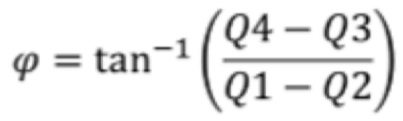
當確定相位差φ時,可以根據光速(例如,光常數c)和調變信號的頻率fmod來計算距離(Distance)。When determining the phase difference φ, the distance (Distance) can be calculated according to the speed of light (for example, the optical constant c) and the frequency fmod of the modulated signal.
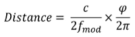
另外,可以基於像素資訊Q1、Q2、Q3、Q4來估計調變信號的幅度(Amplitude)。In addition, the amplitude of the modulated signal can be estimated based on the pixel information Q1, Q2, Q3, and Q4.

透過上述方式,TOF感測系統100可以確定調變信號的頻率或幅度,並計算TOF感測系統100與目標20之間的距離。根據實施方式,可以根據TOF感測系統100的環境來改變調變信號的頻率或幅度。Through the above method, the
另一方面,在TOF感測系統100的操作中,由於可以基於與調變信號相關聯的每個相移信號來準確地輸出回應於反射信號而生成的電荷量,因此可以減小距離誤差並且能夠增加深度資訊的解析度。On the other hand, in the operation of the
如圖1中所描述的,存在調變信號和反射信號,以及來自TOF感測系統100工作的環境的自然光或環境光。例如,在TOF感測系統100中使用的調變信號可以具有在紫外區域或紅外區域中的頻帶。調變信號還可以具有與任何自然光或光信號相同的頻率。即使第二透鏡單元180、280可以具有過濾器,具有紫外區域或紅外區域中的相應頻帶的自然光或環境光可以輸入至TOF感測系統100。自然光或環境光可以充當雜訊和干擾。因此,當TOF感測系統100在白天戶外使用時,接收器120、220可能由於自然光或環境光的存在而接收過多的入射光。如果過多的入射光輸入至接收器,則TOF感測系統100可能沒有用於計算或估計到目標的距離或目標的深度資訊的操作裕量。As described in FIG. 1, there are modulated signals and reflected signals, as well as natural light or ambient light from the environment in which the
圖8例示了當安裝在根據本公開的實施方式的TOF感測系統中的圖像感測器操作時發生的延遲。FIG. 8 illustrates a delay that occurs when the image sensor installed in the TOF sensing system according to the embodiment of the present disclosure operates.
參照圖8,圖像感測器520可以包括:包括多個像素128的像素陣列126;以及被配置為驅動像素陣列126的驅動電路122。參照圖5,在像素陣列126中,多個像素128可以沿著多個列和多個行佈置。8, the
驅動電路122可以向每個像素128中的轉移閘TG或TG1、TG2提供驅動控制信號(例如,設定的導通電壓)以使轉移閘TG或TG1、TG2導通。驅動電路122可以回應於時脈信號Clk或調變信號來確定提供給每個像素128的驅動控制信號的相位。The driving
參照圖8,假設從驅動電路122輸出的驅動控制信號提供給像素陣列126中沿著一行佈置的每個像素的轉移閘。理想地,驅動控制信號同時提供給所有像素的轉移閘。然而,實際上,在傳送驅動控制信號的行線中可能發生延遲。因此,在驅動控制信號被提供到最接近驅動電路122的位置處的像素的轉移閘TXnear的時間與驅動控制信號被提供到在距離驅動電路122最遠位置處的像素的轉移閘TXfar的時間之間可以出現時間差。在這種情況下,傳送驅動控制信號的時間差可能會影響像素的操作區段(例如,像素驅動時間),每個像素回應於反射信號而生成並輸出一定量的電荷。Referring to FIG. 8, it is assumed that the driving control signal output from the driving
在像素陣列126內,即使分別定位為最接近驅動電路122的和最遠離驅動電路122的兩個像素接收到的反射信號是相同的(即,從兩個像素到目標20的實際距離是相同的),當兩個像素的操作區段之間依據它們相對於驅動電路126的位置而存在由延遲引起的時間差時,所計算的距離也可能不同。參照圖6和圖7,因為時間差可以使基於由每個像素接收的反射信號與從發射器輸出的調變信號之間的相位關係而發生的相位差失真,所以時間差可以影響計算出的距離。In the
具體地,當TOF感測系統100可以執行操作以透過幾個階段(例如,在調變信號和反射信號的幾個週期期間)更準確地計算或估計TOF感測系統100與目標20之間的距離時,透過兩個像素(即,像素陣列126中定位為最遠離驅動電路122的像素和最接近驅動電路122的像素)可以識別的反射信號的量中的失真可以變得更嚴重(例如,由於失真引起的差可以更大)。換句話說,在每階段中由圖像感測器520感測的反射信號的量越大,由最接近的像素和最遠離的像素單獨感測到的反射信號的量之和之間的差越大,如下式所示。Specifically, when the
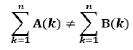


因此,在TOF感測系統中,用於在幾個週期期間計算距離以獲得更準確距離的測量方法可能導致獲得更不正確的距離。Therefore, in the TOF sensing system, the measurement method used to calculate the distance during several cycles to obtain a more accurate distance may result in obtaining a more incorrect distance.
為了克服該問題,可以建議增加傳送提供給每個像素的轉移閘的驅動控制信號(例如,設定電壓)的行線的尺寸(即,寬度或厚度)。增加行線的尺寸可以減小行線的電阻,從而減小的電阻可以減小行線中的延遲。該方法具有減小行線的電阻和經由行線傳送驅動控制信號的延遲的效果,但是可能影響圖像感測器的整合(integration),並且在製造圖像感測器的微處理中引發使行線尺寸變大的負擔。In order to overcome this problem, it may be suggested to increase the size (ie, width or thickness) of the row line that transmits the drive control signal (for example, set voltage) of the transfer gate provided to each pixel. Increasing the size of the row line can reduce the resistance of the row line, so that the reduced resistance can reduce the delay in the row line. This method has the effect of reducing the resistance of the row line and the delay of transmitting the driving control signal via the row line, but may affect the integration of the image sensor, and cause the use of micro-processing in the manufacturing of the image sensor. The line size becomes larger.
圖9A至圖9D示出了用於避免或克服安裝在根據本公開的實施方式的TOF感測系統中的圖像感測器工作時發生的延遲的示例。在圖9A至圖9D中,可以改變向其提供驅動控制信號的像素的順序,以補償當透過行線傳送從驅動電路輸出的驅動控制信號時發生的延遲。根據實施方式,像素陣列326A、326B、326C、326D可以包括多個像素,每個像素被提供有從圖9A至圖9D所示的驅動電路輸出的驅動控制信號。像素陣列326A至326D可以包括如參照圖6所描述的一對第一相位接收器328A和第二相位接收器328B,一對第一相位接收器328A和第二相位接收器328B各自能夠基於驅動控制信號的相反相位回應於入射光而生成並輸出一定量的電荷。9A to 9D show examples for avoiding or overcoming the delay that occurs when the image sensor installed in the TOF sensing system according to the embodiment of the present disclosure operates. In FIGS. 9A to 9D, the order of pixels to which drive control signals are supplied can be changed to compensate for the delay that occurs when the drive control signals output from the drive circuit are transmitted through the row lines. According to an embodiment, the
參照圖9A,每對奇數行線和偶數行線可以在像素陣列326A的一側聯接,而驅動電路322A在像素陣列326A的相對側向像素陣列326A提供驅動控制信號。對於每個對,從驅動電路322A輸出的驅動控制信號可以被提供給在像素陣列326A的一側的奇數行的端子,然後在像素陣列326A的相對側被傳送給偶數行的端子。考慮到操作或驅動時間,驅動控制信號可以首先提供給奇數行中最接近驅動電路322A的像素中的轉移閘,並且驅動控制信號可以最後提供給偶數行中最接近驅動電路322A的像素的轉移閘。在這兩個驅動時間極限之間,驅動控制信號可以提供給在奇數行和偶數行中距驅動電路322A最遠的像素的轉移閘。在這種情況下,如果組合在一對奇數行和偶數行的同一列上相鄰佈置的兩個像素的感測量,則在列之間一對奇數行和偶數行的兩個像素的感測量可以沒有差異,從而圖像感測器520可以補償由於每個像素距聯接至像素陣列326A的驅動電路322A的距離不同而引起的延遲。例如,TOF感測系統100可以使用每列中的兩個相鄰像素的組合像素資訊來計算TOF感測系統100與目標20之間的距離。因此,因為每列中兩個相鄰像素的延遲之和可以基本上彼此相同,所以可以補償傳送驅動控制信號的延遲。儘管每個像素相對於驅動電路322A位於不同位置,但是圖9A所示的該方案可以補償像素之間的距驅動電路322A的不同距離。9A, each pair of odd and even row lines may be coupled on one side of the
參照圖9B,每對奇數行線和偶數行線可以在像素陣列326B的一側聯接,而驅動電路322B在像素陣列326B的相對側向像素陣列326B提供驅動控制信號。對於每個對,從驅動電路322B輸出的驅動控制信號可以被提供給像素陣列326B的一側的偶數行的端子,然後在像素陣列326B的相對側被傳送給奇數行的端子。考慮到操作或驅動時間,驅動控制信號可以首先提供給偶數行中最接近驅動電路322B的像素中的轉移閘,並且驅動控制信號可以最後提供給奇數行中最接近驅動電路322B的像素中的轉移閘。在這兩個驅動時間極限之間,驅動控制信號可以傳遞到在奇數行和偶數行中距驅動電路322B最遠的像素的轉移閘。類似於圖9A中所示的方案,每列中的一對奇數行和偶數行的兩個相鄰像素的感測量之和可以基本相同,從而可以補償由每列與驅動電路322B之間的不同距離而引起的延遲差。在圖9B所示的方案中,在每列中發生的平均延遲可以基本相同,使得圖像感測器520可以避免由列之間的延遲不同而誘發的失真。9B, each pair of odd and even row lines may be coupled on one side of the
參照圖9C,圖像感測器520可以包括設置在像素陣列326C的兩側(即,相對兩側)的第一驅動電路322C和第二驅動電路324C。詳細地,第一驅動電路322C和第二驅動電路324C可以向像素陣列326C中的多個像素的轉移閘單獨地提供第一驅動控制信號和第二驅動控制信號。從第一驅動電路322C和第二驅動電路324C單獨輸出的第一驅動控制信號和第二驅動控制信號沿相對方向向像素陣列326C傳送。第一驅動電路322C可以向佈置在像素陣列326C的奇數行上的奇數像素提供第一驅動控制信號,而第二驅動電路324C可以向佈置在像素陣列326C的偶數行上的偶數像素提供第二驅動控制信號。在本文中,第一驅動控制信號和第二驅動控制信號可以具有基本相同的相位。儘管在奇數行和偶數行二者中可以發生延遲,但是一對奇數行和偶數行的同一列中的兩個相鄰像素的感測量可以組合以補償由從給定列分別到第一驅動電路322C和第二驅動電路324C的不同距離而引起的延遲。可以基於從第一驅動電路322C和第二驅動電路324C中的一個到像素的距離來確定延遲量。在這種情況下,一對奇數行和偶數行的每一列中的兩個相鄰像素與第一驅動電路322C和第二驅動電路324C之間的距離之和可以彼此相同,從而可以避免由於像素之間的延遲差而引起的失真。根據實施方式,從佈置在奇數行線中的像素和佈置在偶數行線中的另一像素各自輸出的像素資訊可以組合或求和,以補償延遲差。9C, the
參照圖9D,圖像感測器520可以包括分別設置在像素陣列326D的上側和下側(即,相對兩側)的第一驅動電路322D和第二驅動電路324D。詳細地,第一驅動電路322D和第二驅動電路324D可以分別向像素陣列326D中的多個像素的轉移閘各自提供第一驅動控制信號和第二驅動控制信號。第一驅動控制信號和第二驅動控制信號沿相對方向傳送至像素陣列326D。第一驅動電路322D可以向佈置在像素陣列326D的偶數行上的偶數像素提供第一驅動控制信號,而第二驅動電路324D可以向佈置在像素陣列326D的奇數行上的奇數像素提供第二驅動控制信號。在本文中,第一驅動控制信號和第二驅動控制信號可以具有基本相同的相位。儘管在奇數行和偶數行二者中可以發生延遲,但是在一對奇數行和偶數行的同一列中的兩個相鄰像素的感測量可以組合以補償由從第一驅動電路322D和第二驅動電路324D到每列的距離不同而引起的延遲。可以基於像素與第一驅動電路322D和第二驅動電路324D中的一個之間的距離來確定延遲量。在這種情況下,在一對奇數行和偶數行的每一列中的兩個相鄰像素之間,距第一驅動電路322D和第二驅動電路324D的距離之和可以彼此相同,使得可以避免由上述延遲引起的失真。9D, the
在圖9D中,第一驅動電路322D和第二驅動電路324D可以設置在像素陣列326D的兩側(相對兩側)上。像圖9C所示的方案一樣,第一驅動電路322D和第二驅動電路324D可以向像素陣列326D中的多個像素的轉移閘各自提供第一驅動控制信號和第二驅動控制信號。第一驅動控制信號和第二驅動控制信號沿相對方向傳送至像素陣列326D。第一驅動電路322D可以向像素陣列326D的偶數行提供第一驅動控制信號,而第二驅動電路324D可以向像素陣列326D的奇數行提供第二驅動控制信號。像素陣列326D的每一列中的兩個相鄰像素與第一驅動電路322D和第二驅動電路324D之間的距離之和可以彼此相同。即使在偶數行和奇數行二者中各自發生延遲,但是可以去除像素陣列326D的列之間的延遲差。因此,可以減少由於像素之間的延遲差引起的失真。In FIG. 9D, the
圖10例示了針對在圖像感測器操作的同時的延遲透過圖9A至圖9D中描述的示例而改進的性能。FIG. 10 illustrates improved performance for delay through the examples described in FIGS. 9A to 9D while the image sensor is operating.
參照圖10,由於延遲,驅動控制信號提供到不同像素的時間可能不相同。即使驅動控制信號是相同信號,提供到在最接近驅動電路的位置處的像素的轉移閘TXnear與提供到在最遠離驅動電路的位置處的像素的轉移閘TXfar的驅動控制信號之間也可能存在相位差。如圖9A至圖9D所示,可以改變向像素提供驅動控制信號的順序,以補償傳送從驅動電路輸出的驅動控制信號的延遲。例如,當兩個像素與從驅動電路各自提供給最接近驅動電路的像素的轉移閘TXnear和最遠離驅動電路的像素的轉移閘TXfar二者的驅動控制信號相關聯時,整合從兩個像素輸出的像素資訊可以具有基本相同的延遲補償效果。Referring to FIG. 10, due to the delay, the time at which the driving control signal is supplied to different pixels may not be the same. Even if the drive control signal is the same signal, there may be between the transfer gate TXnear supplied to the pixel at the position closest to the drive circuit and the drive control signal supplied to the transfer gate TXfar of the pixel at the position farthest from the drive circuit. Phase difference. As shown in FIGS. 9A to 9D, the order of supplying driving control signals to the pixels may be changed to compensate for the delay in transmitting the driving control signals output from the driving circuit. For example, when two pixels are associated with the drive control signals of the transfer gate TXnear of the pixel closest to the drive circuit and the transfer gate TXfar of the pixel furthest away from the drive circuit, respectively, the output from the two pixels is integrated. The pixel information can have basically the same delay compensation effect.
在圖10中,可以整合在多階段中各自位於最接近和最遠離驅動電路的位置處的像素的操作區段,以避免失真。例如,在驅動控制信號的第一時段中被驅動的具有轉移閘TXnear的像素的操作區段可以與在第二時段中被驅動的具有轉移閘TXfar的像素的另一操作區段整合。此外,在另一實施方式中,可以組合在驅動控制信號的相同時段中被驅動的具有轉移閘TXnear和轉移閘TXfar的像素的操作區段。參照圖9A和圖9B,在驅動控制信號的第一時段中被驅動的具有轉移閘TXnear的像素的操作區段可以與在第一時段中被驅動的具有轉移閘TXfar的像素的另一操作區段整合。In FIG. 10, it is possible to integrate the operation sections of the pixels each located at the positions closest to and farthest from the driving circuit in multiple stages to avoid distortion. For example, the operation section of the pixel with the transfer gate TXnear that is driven in the first period of the drive control signal may be integrated with another operation section of the pixel with the transfer gate TXfar that is driven in the second period. Furthermore, in another embodiment, the operation sections of the pixels having the transfer gate TXnear and the transfer gate TXfar that are driven in the same period of the drive control signal may be combined. 9A and 9B, the operation area of the pixel with the transfer gate TXnear driven in the first period of the drive control signal may be the same as the other operation area of the pixel with the transfer gate TXfar driven in the first period. Segment integration.
如圖8中所描述的,隨著感測持續多個時段或多階段,各自位於最接近驅動電路和最遠離驅動電路的位置處的像素的操作區段之間的差異可能增大。然而,在那種情況下,可以在幾個時段上整合從兩個像素輸出的像素資訊。因此,即使當由圖像感測器520感測到的反射信號的量增加時,也可以去除從位於最遠離和最接近的像素各自輸出的反射信號量之和之間的差異。因此,信號整合(例如,像素資訊整合)可以去除差異,如下式所示。As described in FIG. 8, as the sensing continues for multiple periods or multiple stages, the difference between the operation sections of the pixels each located closest to the drive circuit and farthest from the drive circuit may increase. However, in that case, the pixel information output from the two pixels can be integrated over several periods. Therefore, even when the amount of the reflection signal sensed by the
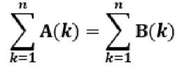


儘管像素陣列中的像素位置可能引起驅動控制信號的傳送延遲,但是本方案可以補償延遲。本方案可能主要不是防止取決於與每個像素和驅動電路之間的不同距離相對應的不同操作區段的延遲。然而,本方案可以提供一種透過信號整合來補償延遲的方式。TOF感測系統可以避免由於取決於像素在像素陣列中的位置的、像素的操作區段之間的差異而引起的失真。Although the pixel position in the pixel array may cause the transmission delay of the drive control signal, this solution can compensate for the delay. This solution may not mainly prevent delays depending on different operation sections corresponding to different distances between each pixel and the driving circuit. However, this solution can provide a way to compensate for the delay through signal integration. The TOF sensing system can avoid distortion caused by the difference between the operation sections of the pixel depending on the position of the pixel in the pixel array.
根據本公開的實施方式,飛行時間(TOF)感測系統能夠更準確地測量距場景中的目標或物體的距離,從而生成包括關於場景中的目標或物體的深度資訊的三維(3D)圖像。According to an embodiment of the present disclosure, a time-of-flight (TOF) sensing system can more accurately measure the distance to a target or object in the scene, thereby generating a three-dimensional (3D) image including depth information about the target or object in the scene .
另外,本公開的實施方式能夠提供一種圖像感測器,該圖像感測器被配置為補償驅動電壓的提供延遲,該延遲可以根據每個像素在像素陣列中的位置或方位而不同地確定。每個像素可以回應於從目標或物體反射的入射光而生成一定量的電荷。可以以在每個像素處提供驅動電壓的位置為基礎來補償驅動電壓的提供延遲。在提供深度資訊以生成三維(3D)圖像的TOF感測系統中,基於像素之間的驅動電壓的提供順序來補償延遲的圖像感測器可以比採用單獨信號處理演算法的配置比提供更有效且更快的延遲補償。In addition, the embodiments of the present disclosure can provide an image sensor configured to compensate for the supply delay of the driving voltage, and the delay may be different according to the position or orientation of each pixel in the pixel array. determine. Each pixel can generate a certain amount of charge in response to incident light reflected from a target or object. The supply delay of the driving voltage can be compensated on the basis of the position where the driving voltage is supplied at each pixel. In a TOF sensing system that provides depth information to generate a three-dimensional (3D) image, an image sensor that compensates for delay based on the sequence of providing driving voltages between pixels can be provided more than a configuration using a separate signal processing algorithm More effective and faster delay compensation.
雖然已經針對特定實施方式例示並描述了本發明,但是本發明所屬技術領域中具有通常知識者在本公開的教示下將顯而易見的是,在不脫離如以下請求項所定義的本公開的精神和範圍的情況下,可以進行各種變型和修改。本發明涵蓋落入請求項範圍內的所有變型和修改。Although the present invention has been illustrated and described for specific embodiments, it will be obvious to those with ordinary knowledge in the technical field to which the present invention pertains under the teachings of the present disclosure that without departing from the spirit and spirit of the present disclosure as defined by the following claims In the case of the scope, various modifications and modifications can be made. The present invention covers all variations and modifications falling within the scope of the claims.
20:目標
100:TOF感測系統
100A:TOF感測系統
100B:TOF感測系統
110:發射器
120:接收器
122:驅動器
126:像素陣列
128:像素
128A:像素
128B:像素
130:信號處理器
140:調變單元
142:調變控制器
144:發射器驅動器
150:解調器
152:相位信號發生器
154:驅動器
160:信號轉換器
170:第一透鏡單元
180:第二透鏡單元
210:發射器
220:接收器
230:信號處理器
244:發射器驅動器
250:解調器
252:相位信號發生器
254:驅動器
260:信號轉換器
270:第一透鏡單元
280:第二透鏡單元
322A:驅動電路
322B:驅動電路
322C:第一驅動電路
322D:第一驅動電路
324C:第二驅動電路
324D:第二驅動電路
326A:像素陣列
326B:像素陣列
326C:像素陣列
326D:像素陣列
328A:第一相位接收器
328B:第二相位接收器
520:圖像感測器
ADC:信號轉換器
C1:相移信號
C2:相移信號
C3:相移信號
C4:相移信號
Clk:時脈信號
D:光接收元件
D1:光接收元件
D2:光接收元件
DC:發射控制信號
DD:數位資料
FC:調變週期信號
MC:調變控制信號
PFC:相位資訊
PI:像素資訊
TC:驅動控制信號
TG:轉移閘
TG1:轉移閘
TG2:轉移閘
TXnear
:在最接近驅動電路的位置處的像素的轉移閘
TXfar
:在最遠離驅動電路的位置處的像素的轉移閘
Q1:第一像素資訊
Q2:第二像素資訊
Q3:第三像素資訊
Q4:第四像素資訊20: Target 100:
本文的描述參考了附圖,其中在整個附圖中,相似的元件符號指代相似的部件。 [圖1]例示了根據本公開的實施方式的飛行時間(TOF)感測系統的操作。 [圖2A和圖2B]示出了根據本公開的實施方式的TOF感測系統中的測量值的示例。 [圖3]例示了根據本公開的實施方式的TOF感測系統的第一示例。 [圖4]例示了根據本公開的實施方式的TOF感測系統的第二示例。 [圖5]示出了根據本公開的實施方式的與TOF感測系統一起配備的圖像感測器中所包括的像素的示例。 [圖6]例示了根據本公開的實施方式的TOF感測系統中所包括的圖像感測器的操作。 [圖7]描述了根據本公開的實施方式的TOF感測系統中的估計距離的方法和確定調變信號的幅度的方法。 [圖8]例示了在安裝於根據本公開的實施方式的TOF感測系統中的圖像感測器操作的同時發生的延遲。 [圖9A至圖9D]例示了用於避免或克服在安裝於根據本公開的實施方式的TOF感測系統中的圖像感測器操作的同時發生的延遲的示例。 [圖10]例示了針對在圖像感測器操作的同時的延遲透過圖9A至圖9D中描述的示例而改進的性能。The description herein refers to the accompanying drawings, in which similar reference numerals refer to similar components throughout the drawings. [FIG. 1] Illustrates the operation of a time of flight (TOF) sensing system according to an embodiment of the present disclosure. [FIG. 2A and FIG. 2B] show examples of measured values in the TOF sensing system according to the embodiment of the present disclosure. [FIG. 3] Illustrates a first example of a TOF sensing system according to an embodiment of the present disclosure. [FIG. 4] Illustrates a second example of the TOF sensing system according to the embodiment of the present disclosure. [FIG. 5] shows an example of pixels included in an image sensor equipped with a TOF sensing system according to an embodiment of the present disclosure. [FIG. 6] Illustrates the operation of the image sensor included in the TOF sensing system according to the embodiment of the present disclosure. [FIG. 7] Describes the method of estimating the distance and the method of determining the amplitude of the modulated signal in the TOF sensing system according to the embodiment of the present disclosure. [FIG. 8] Illustrates the delay that occurs while the image sensor installed in the TOF sensing system according to the embodiment of the present disclosure is operating. [FIG. 9A to FIG. 9D] illustrates an example for avoiding or overcoming the delay that occurs while operating the image sensor installed in the TOF sensing system according to the embodiment of the present disclosure. [FIG. 10] illustrates the improved performance through the examples described in FIGS. 9A to 9D for the delay while the image sensor is operating.
20:目標20: goal
100:TOF感測系統100: TOF sensing system
110:發射器110: Launcher
120:接收器120: receiver
Claims (20)
Applications Claiming Priority (2)
| Application Number | Priority Date | Filing Date | Title |
|---|---|---|---|
| KR10-2019-0162790 | 2019-12-09 | ||
| KR1020190162790A KR103004447B1 (en) | 2019-12-09 | Time of flight sensing system, image sensor |
Publications (2)
| Publication Number | Publication Date |
|---|---|
| TW202127635A true TW202127635A (en) | 2021-07-16 |
| TWI897871B TWI897871B (en) | 2025-09-21 |
Family
ID=76210886
Family Applications (2)
| Application Number | Title | Priority Date | Filing Date |
|---|---|---|---|
| TW109124423A TWI897871B (en) | 2019-12-09 | 2020-07-20 | Time of flight sensing system and image sensor used therein |
| TW113150837A TWI898971B (en) | 2019-12-09 | 2020-07-20 | Image sensor used in time of flight sensing system |
Family Applications After (1)
| Application Number | Title | Priority Date | Filing Date |
|---|---|---|---|
| TW113150837A TWI898971B (en) | 2019-12-09 | 2020-07-20 | Image sensor used in time of flight sensing system |
Country Status (4)
| Country | Link |
|---|---|
| US (1) | US11709271B2 (en) |
| JP (1) | JP7765174B2 (en) |
| CN (1) | CN112946686B (en) |
| TW (2) | TWI897871B (en) |
Families Citing this family (8)
| Publication number | Priority date | Publication date | Assignee | Title |
|---|---|---|---|---|
| US11693116B2 (en) * | 2020-08-31 | 2023-07-04 | Pixart Imaging Inc. | Distance measurement device using two light modulation frequencies and operating method thereof |
| TWI762387B (en) * | 2021-07-16 | 2022-04-21 | 台達電子工業股份有限公司 | Time of flight devide and inspecting method for the same |
| CN113625303A (en) * | 2021-08-05 | 2021-11-09 | 思特威(上海)电子科技股份有限公司 | Pixel array signal acquisition method, time-of-flight sensor, terminal and medium |
| US11770633B2 (en) * | 2021-10-28 | 2023-09-26 | Omnivision Technologies, Inc. | Readout architecture for indirect time-of-flight sensing |
| CN115396607A (en) * | 2022-08-26 | 2022-11-25 | 天津大学 | TOF imaging 2-tap pixel modulation resolving method |
| US12566273B2 (en) * | 2023-01-18 | 2026-03-03 | Himax Technologies Limited | Time-of-flight 3D sensing system |
| CN116908877B (en) | 2023-06-08 | 2024-09-17 | 信扬科技(佛山)有限公司 | Time-of-flight camera and depth image acquisition method |
| TWI873676B (en) * | 2023-06-08 | 2025-02-21 | 大陸商信揚科技(佛山)有限公司 | Time-of-flight camera and depth image acquisition method |
Family Cites Families (29)
| Publication number | Priority date | Publication date | Assignee | Title |
|---|---|---|---|---|
| US7128270B2 (en) * | 1999-09-17 | 2006-10-31 | Silverbrook Research Pty Ltd | Scanning device for coded data |
| JP2001251557A (en) * | 1999-12-27 | 2001-09-14 | Canon Inc | Area sensor, image input device having the area sensor, and method of driving the area sensor |
| CN1259796C (en) | 2003-12-12 | 2006-06-14 | 北京大学 | A focal plane array readout circuit and its readout method |
| JP4161910B2 (en) | 2004-01-28 | 2008-10-08 | 株式会社デンソー | Distance image data generation device, generation method, and program |
| US7994465B1 (en) | 2006-02-06 | 2011-08-09 | Microsoft Corporation | Methods and devices for improved charge management for three-dimensional and color sensing |
| JP5404112B2 (en) | 2009-03-12 | 2014-01-29 | キヤノン株式会社 | Solid-state imaging device, driving method thereof, and imaging system |
| FR2961019B1 (en) * | 2010-06-03 | 2013-04-12 | Commissariat Energie Atomique | LINEAR IMAGE SENSOR IN CMOS TECHNOLOGY |
| US20120154535A1 (en) | 2010-12-15 | 2012-06-21 | Microsoft Corporation | Capturing gated and ungated light in the same frame on the same photosurface |
| US8854433B1 (en) * | 2012-02-03 | 2014-10-07 | Aquifi, Inc. | Method and system enabling natural user interface gestures with an electronic system |
| US8836768B1 (en) * | 2012-09-04 | 2014-09-16 | Aquifi, Inc. | Method and system enabling natural user interface gestures with user wearable glasses |
| KR101444014B1 (en) * | 2013-03-07 | 2014-09-23 | 주식회사 동부하이텍 | Operating circuit of image sensor and operating method thereof |
| WO2015120328A1 (en) * | 2014-02-07 | 2015-08-13 | Rambus Inc. | Feedthrough-compensated image sensor |
| US9720076B2 (en) * | 2014-08-29 | 2017-08-01 | Omnivision Technologies, Inc. | Calibration circuitry and method for a time of flight imaging system |
| US20160205378A1 (en) * | 2015-01-08 | 2016-07-14 | Amir Nevet | Multimode depth imaging |
| JP6773029B2 (en) | 2015-04-24 | 2020-10-21 | ソニー株式会社 | Solid-state image sensor, semiconductor device, and electronic device |
| US9819930B2 (en) * | 2015-05-26 | 2017-11-14 | Omnivision Technologies, Inc. | Time of flight imaging with improved initiation signaling |
| DE102015112398A1 (en) * | 2015-07-29 | 2017-02-02 | Infineon Technologies Ag | An image forming apparatus and image forming method for acquiring image forming data over a pixel array |
| EP3418772A4 (en) | 2016-02-17 | 2019-03-13 | Panasonic Intellectual Property Management Co., Ltd. | DISTANCE MEASURING DEVICE |
| JP6650309B2 (en) * | 2016-03-24 | 2020-02-19 | スタンレー電気株式会社 | Distance measuring device |
| DE102016208347B4 (en) * | 2016-05-13 | 2017-12-21 | Infineon Technologies Ag | An optical sensor device and method for operating a runtime sensor |
| WO2018101187A1 (en) | 2016-11-29 | 2018-06-07 | パナソニックIpマネジメント株式会社 | Distance measuring device |
| US10616519B2 (en) * | 2016-12-20 | 2020-04-07 | Microsoft Technology Licensing, Llc | Global shutter pixel structures with shared transfer gates |
| CN106842227B (en) * | 2017-03-07 | 2019-04-16 | 中国科学院大学 | Precision optics distance measuring method based on zero refractive index Meta Materials |
| KR102398025B1 (en) * | 2017-03-15 | 2022-05-17 | 에스케이하이닉스 주식회사 | Image sensor |
| EP3474038B1 (en) * | 2017-10-23 | 2024-07-24 | ams International AG | Image sensor for determining a three-dimensional image and method for determining a three-dimensional image |
| CN111684304B (en) * | 2017-12-04 | 2024-06-04 | ams国际有限公司 | Distance flight time module |
| KR102488321B1 (en) * | 2017-12-29 | 2023-01-13 | 삼성전자주식회사 | Pixel array included in three-dimensional image sensor and method of operating three-dimensional image sensor |
| KR102473650B1 (en) * | 2018-04-13 | 2022-12-02 | 엘지이노텍 주식회사 | Camera module and depth map extraction method of the same |
| US10914823B2 (en) * | 2018-05-01 | 2021-02-09 | Qualcomm Incorporated | Time of flight ranging with varying fields of emission |
-
2020
- 2020-06-02 US US16/890,170 patent/US11709271B2/en active Active
- 2020-07-20 TW TW109124423A patent/TWI897871B/en active
- 2020-07-20 TW TW113150837A patent/TWI898971B/en active
- 2020-07-22 CN CN202010708609.XA patent/CN112946686B/en active Active
- 2020-11-13 JP JP2020189493A patent/JP7765174B2/en active Active
Also Published As
| Publication number | Publication date |
|---|---|
| CN112946686B (en) | 2024-08-16 |
| CN112946686A (en) | 2021-06-11 |
| JP2021092554A (en) | 2021-06-17 |
| JP7765174B2 (en) | 2025-11-06 |
| KR20210072458A (en) | 2021-06-17 |
| US20210173086A1 (en) | 2021-06-10 |
| TW202517087A (en) | 2025-04-16 |
| US11709271B2 (en) | 2023-07-25 |
| TWI898971B (en) | 2025-09-21 |
| TWI897871B (en) | 2025-09-21 |
Similar Documents
| Publication | Publication Date | Title |
|---|---|---|
| TWI898971B (en) | Image sensor used in time of flight sensing system | |
| CN113030999B (en) | Time-of-flight sensing system and image sensor for use therein | |
| KR101711061B1 (en) | Method for estimating depth information using depth estimation device | |
| CN206650757U (en) | a device | |
| CN113970757B (en) | A depth imaging method and a depth imaging system | |
| KR101565969B1 (en) | Method and device for estimating depth information and signal processing apparatus having the device | |
| CN101449181B (en) | Distance measuring method and distance measuring instrument for detecting the spatial dimension of a target | |
| WO2021008209A1 (en) | Depth measurement apparatus and distance measurement method | |
| WO2021120403A1 (en) | Depth measurement device and method | |
| CN110471080A (en) | Depth measurement device based on TOF imaging sensor | |
| WO2021051478A1 (en) | Time-of-flight-based distance measurement system and method for dual-shared tdc circuit | |
| KR20160032014A (en) | A method for driving a time-of-flight system | |
| WO2021051479A1 (en) | Interpolation-based time of flight measurement method and system | |
| CN111758047A (en) | Single-chip RGB-D camera | |
| WO2019179123A1 (en) | Tof camera and design method for diffractive optical element | |
| IL269455B2 (en) | Time of flight sensor | |
| WO2023120009A1 (en) | Ranging device, and sensor device | |
| Martin et al. | An all-in-one 64-zone SPAD-based direct-time-of-flight ranging sensor with embedded illumination | |
| KR20220081056A (en) | Image sensing device and operating method thereof | |
| CN114706057B (en) | Transmitting modules, TOF devices and electronic equipment | |
| CN119596332A (en) | Image sensing apparatus, image processing apparatus, and imaging apparatus | |
| WO2021248292A1 (en) | Time of flight-based distance measurement method and related distance measurement system |