TW202242547A - Patterning stack - Google Patents
Patterning stack Download PDFInfo
- Publication number
- TW202242547A TW202242547A TW111106651A TW111106651A TW202242547A TW 202242547 A TW202242547 A TW 202242547A TW 111106651 A TW111106651 A TW 111106651A TW 111106651 A TW111106651 A TW 111106651A TW 202242547 A TW202242547 A TW 202242547A
- Authority
- TW
- Taiwan
- Prior art keywords
- layer
- top coating
- coating layer
- material layer
- substituted
- Prior art date
Links
Images


Classifications
-
- G—PHYSICS
- G03—PHOTOGRAPHY; CINEMATOGRAPHY; ANALOGOUS TECHNIQUES USING WAVES OTHER THAN OPTICAL WAVES; ELECTROGRAPHY; HOLOGRAPHY
- G03F—PHOTOMECHANICAL PRODUCTION OF TEXTURED OR PATTERNED SURFACES, e.g. FOR PRINTING, FOR PROCESSING OF SEMICONDUCTOR DEVICES; MATERIALS THEREFOR; ORIGINALS THEREFOR; APPARATUS SPECIALLY ADAPTED THEREFOR
- G03F7/00—Photomechanical, e.g. photolithographic, production of textured or patterned surfaces, e.g. printing surfaces; Materials therefor, e.g. comprising photoresists; Apparatus specially adapted therefor
- G03F7/004—Photosensitive materials
- G03F7/09—Photosensitive materials characterised by structural details, e.g. supports, auxiliary layers
- G03F7/091—Photosensitive materials characterised by structural details, e.g. supports, auxiliary layers characterised by antireflection means or light filtering or absorbing means, e.g. anti-halation, contrast enhancement
-
- G—PHYSICS
- G03—PHOTOGRAPHY; CINEMATOGRAPHY; ANALOGOUS TECHNIQUES USING WAVES OTHER THAN OPTICAL WAVES; ELECTROGRAPHY; HOLOGRAPHY
- G03F—PHOTOMECHANICAL PRODUCTION OF TEXTURED OR PATTERNED SURFACES, e.g. FOR PRINTING, FOR PROCESSING OF SEMICONDUCTOR DEVICES; MATERIALS THEREFOR; ORIGINALS THEREFOR; APPARATUS SPECIALLY ADAPTED THEREFOR
- G03F7/00—Photomechanical, e.g. photolithographic, production of textured or patterned surfaces, e.g. printing surfaces; Materials therefor, e.g. comprising photoresists; Apparatus specially adapted therefor
- G03F7/004—Photosensitive materials
-
- G—PHYSICS
- G03—PHOTOGRAPHY; CINEMATOGRAPHY; ANALOGOUS TECHNIQUES USING WAVES OTHER THAN OPTICAL WAVES; ELECTROGRAPHY; HOLOGRAPHY
- G03F—PHOTOMECHANICAL PRODUCTION OF TEXTURED OR PATTERNED SURFACES, e.g. FOR PRINTING, FOR PROCESSING OF SEMICONDUCTOR DEVICES; MATERIALS THEREFOR; ORIGINALS THEREFOR; APPARATUS SPECIALLY ADAPTED THEREFOR
- G03F7/00—Photomechanical, e.g. photolithographic, production of textured or patterned surfaces, e.g. printing surfaces; Materials therefor, e.g. comprising photoresists; Apparatus specially adapted therefor
- G03F7/004—Photosensitive materials
- G03F7/075—Silicon-containing compounds
- G03F7/0752—Silicon-containing compounds in non photosensitive layers or as additives, e.g. for dry lithography
-
- G—PHYSICS
- G03—PHOTOGRAPHY; CINEMATOGRAPHY; ANALOGOUS TECHNIQUES USING WAVES OTHER THAN OPTICAL WAVES; ELECTROGRAPHY; HOLOGRAPHY
- G03F—PHOTOMECHANICAL PRODUCTION OF TEXTURED OR PATTERNED SURFACES, e.g. FOR PRINTING, FOR PROCESSING OF SEMICONDUCTOR DEVICES; MATERIALS THEREFOR; ORIGINALS THEREFOR; APPARATUS SPECIALLY ADAPTED THEREFOR
- G03F7/00—Photomechanical, e.g. photolithographic, production of textured or patterned surfaces, e.g. printing surfaces; Materials therefor, e.g. comprising photoresists; Apparatus specially adapted therefor
- G03F7/004—Photosensitive materials
- G03F7/09—Photosensitive materials characterised by structural details, e.g. supports, auxiliary layers
- G03F7/094—Multilayer resist systems, e.g. planarising layers
-
- G—PHYSICS
- G03—PHOTOGRAPHY; CINEMATOGRAPHY; ANALOGOUS TECHNIQUES USING WAVES OTHER THAN OPTICAL WAVES; ELECTROGRAPHY; HOLOGRAPHY
- G03F—PHOTOMECHANICAL PRODUCTION OF TEXTURED OR PATTERNED SURFACES, e.g. FOR PRINTING, FOR PROCESSING OF SEMICONDUCTOR DEVICES; MATERIALS THEREFOR; ORIGINALS THEREFOR; APPARATUS SPECIALLY ADAPTED THEREFOR
- G03F7/00—Photomechanical, e.g. photolithographic, production of textured or patterned surfaces, e.g. printing surfaces; Materials therefor, e.g. comprising photoresists; Apparatus specially adapted therefor
- G03F7/004—Photosensitive materials
- G03F7/09—Photosensitive materials characterised by structural details, e.g. supports, auxiliary layers
- G03F7/095—Photosensitive materials characterised by structural details, e.g. supports, auxiliary layers having more than one photosensitive layer
-
- G—PHYSICS
- G03—PHOTOGRAPHY; CINEMATOGRAPHY; ANALOGOUS TECHNIQUES USING WAVES OTHER THAN OPTICAL WAVES; ELECTROGRAPHY; HOLOGRAPHY
- G03F—PHOTOMECHANICAL PRODUCTION OF TEXTURED OR PATTERNED SURFACES, e.g. FOR PRINTING, FOR PROCESSING OF SEMICONDUCTOR DEVICES; MATERIALS THEREFOR; ORIGINALS THEREFOR; APPARATUS SPECIALLY ADAPTED THEREFOR
- G03F7/00—Photomechanical, e.g. photolithographic, production of textured or patterned surfaces, e.g. printing surfaces; Materials therefor, e.g. comprising photoresists; Apparatus specially adapted therefor
- G03F7/004—Photosensitive materials
- G03F7/09—Photosensitive materials characterised by structural details, e.g. supports, auxiliary layers
- G03F7/11—Photosensitive materials characterised by structural details, e.g. supports, auxiliary layers having cover layers or intermediate layers, e.g. subbing layers
-
- H—ELECTRICITY
- H10—SEMICONDUCTOR DEVICES; ELECTRIC SOLID-STATE DEVICES NOT OTHERWISE PROVIDED FOR
- H10D—INORGANIC ELECTRIC SEMICONDUCTOR DEVICES
- H10D30/00—Field-effect transistors [FET]
- H10D30/60—Insulated-gate field-effect transistors [IGFET]
-
- H—ELECTRICITY
- H10—SEMICONDUCTOR DEVICES; ELECTRIC SOLID-STATE DEVICES NOT OTHERWISE PROVIDED FOR
- H10D—INORGANIC ELECTRIC SEMICONDUCTOR DEVICES
- H10D30/00—Field-effect transistors [FET]
- H10D30/60—Insulated-gate field-effect transistors [IGFET]
- H10D30/62—Fin field-effect transistors [FinFET]
-
- H—ELECTRICITY
- H10—SEMICONDUCTOR DEVICES; ELECTRIC SOLID-STATE DEVICES NOT OTHERWISE PROVIDED FOR
- H10P—GENERIC PROCESSES OR APPARATUS FOR THE MANUFACTURE OR TREATMENT OF DEVICES COVERED BY CLASS H10
- H10P76/00—Manufacture or treatment of masks on semiconductor bodies, e.g. by lithography or photolithography
- H10P76/20—Manufacture or treatment of masks on semiconductor bodies, e.g. by lithography or photolithography of masks comprising organic materials
- H10P76/204—Manufacture or treatment of masks on semiconductor bodies, e.g. by lithography or photolithography of masks comprising organic materials of organic photoresist masks
- H10P76/2041—Photolithographic processes
- H10P76/2042—Photolithographic processes using lasers
-
- H—ELECTRICITY
- H10—SEMICONDUCTOR DEVICES; ELECTRIC SOLID-STATE DEVICES NOT OTHERWISE PROVIDED FOR
- H10P—GENERIC PROCESSES OR APPARATUS FOR THE MANUFACTURE OR TREATMENT OF DEVICES COVERED BY CLASS H10
- H10P76/00—Manufacture or treatment of masks on semiconductor bodies, e.g. by lithography or photolithography
- H10P76/20—Manufacture or treatment of masks on semiconductor bodies, e.g. by lithography or photolithography of masks comprising organic materials
- H10P76/204—Manufacture or treatment of masks on semiconductor bodies, e.g. by lithography or photolithography of masks comprising organic materials of organic photoresist masks
- H10P76/2041—Photolithographic processes
- H10P76/2043—Photolithographic processes using an anti-reflective coating
-
- H—ELECTRICITY
- H10—SEMICONDUCTOR DEVICES; ELECTRIC SOLID-STATE DEVICES NOT OTHERWISE PROVIDED FOR
- H10P—GENERIC PROCESSES OR APPARATUS FOR THE MANUFACTURE OR TREATMENT OF DEVICES COVERED BY CLASS H10
- H10P76/00—Manufacture or treatment of masks on semiconductor bodies, e.g. by lithography or photolithography
- H10P76/40—Manufacture or treatment of masks on semiconductor bodies, e.g. by lithography or photolithography of masks comprising inorganic materials
- H10P76/405—Manufacture or treatment of masks on semiconductor bodies, e.g. by lithography or photolithography of masks comprising inorganic materials characterised by their composition, e.g. multilayer masks
Landscapes
- Physics & Mathematics (AREA)
- General Physics & Mathematics (AREA)
- Engineering & Computer Science (AREA)
- Architecture (AREA)
- Structural Engineering (AREA)
- Photosensitive Polymer And Photoresist Processing (AREA)
- Addition Polymer Or Copolymer, Post-Treatments, Or Chemical Modifications (AREA)
- Drying Of Semiconductors (AREA)
Abstract
Description
無none
半導體積體電路(semiconductor integrated circuit,IC)行業經歷了指數級增長。積體電路材料及設計的技術進步產生了一代又一代的積體電路,其中每一世代均具有比上一世代更小且更複雜的電路。在積體電路發展的過程中,功能密度(即,每一晶片面積內的互連裝置的數目)通常提高了,而幾何大小(即,可使用製造製程產生的最小組件(或接線))減小了。這種規模縮小製程通常藉由提高生產效率及降低相關成本來提供益處。此種規模縮小亦增加了積體電路處理及製造的複雜性。The semiconductor integrated circuit (IC) industry has experienced exponential growth. Technological advances in integrated circuit materials and design have produced successive generations of integrated circuits, with each generation having smaller and more complex circuits than the previous generation. During the development of integrated circuits, functional density (i.e., the number of interconnected devices per die area) generally increases while geometry size (i.e., the smallest component (or wiring) that can be produced using a manufacturing process) decreases. small. This scale-down process typically provides benefits by increasing production efficiency and reducing associated costs. Such scaling down also increases the complexity of integrated circuit processing and fabrication.
無none
以下揭示內容提供用於實施所提供標的物的不同特徵的許多不同實施例或實例。組件、值、操作、材料、配置、或類似者的具體實例將在下文描述以簡化本揭露。當然,這些僅為實例且不欲為限制性的。考慮其他組件、值、操作、材料、配置、或類似者。舉例而言,在以下描述中第一特徵於第二特徵上方或上的形成可包含第一及第二特徵直接接觸地形成的實施例,且亦可包含額外特徵可形成於第一特徵與第二特徵之間使得第一特徵及第二特徵可不直接接觸的實施例。另外,本揭露在各種實例中可重複參考數字及/或字母。此重複係出於簡單及清楚的目的,且本身並不指明所論述的各種實施例及/或組態之間的關係。The following disclosure provides many different embodiments, or examples, for implementing different features of the provided subject matter. Specific examples of components, values, operations, materials, configurations, or the like are described below to simplify the present disclosure. Of course, these are examples only and are not intended to be limiting. Consider other components, values, operations, materials, configurations, or the like. For example, in the following description the formation of a first feature over or on a second feature may include embodiments where the first and second features are formed in direct contact, and may also include that additional features may be formed between the first feature and the second feature. An embodiment in which the first feature and the second feature are not in direct contact between the two features. Additionally, the present disclosure may repeat reference numbers and/or letters in various instances. This repetition is for simplicity and clarity and does not in itself indicate a relationship between the various embodiments and/or configurations discussed.
此外,為了方便用於描述如諸圖中圖示的一個元件或特徵與另一(多個)元件或(多個)特徵的關係的描述,在本文中可使用空間相對術語,諸如「在……下面」、「在……之下」、「下部」、「在……之上」、「上部」及類似者。空間相對術語意欲涵蓋除了諸圖中所描繪的定向以外的裝置在使用或操作時的不同定向。裝置可另外定向(舉例而言,旋轉90度或處於其他定向),且本文中所使用的空間相對描述符可類似地加以相應解釋。In addition, in order to facilitate the description for describing the relationship between one element or feature and another element or feature(s) as illustrated in the figures, spatially relative terms may be used herein, such as "in... "below", "beneath", "lower", "above", "upper" and the like. The spatially relative terms are intended to encompass different orientations of the device in use or operation in addition to the orientation depicted in the figures. The device may be otherwise oriented (eg, rotated 90 degrees or at other orientations) and the spatially relative descriptors used herein similarly interpreted accordingly.
光學微影術已用於圖案化基板(例如,晶圓)以形成積體電路的各種特徵。典型的光學微影術製程包含在基板上方塗佈一層光阻劑(或抗蝕劑),將光阻劑曝光於諸如極紫外(extreme ultraviolet,EUV)線的輻射,且顯影及部分剝離光阻劑以在基板上方留下經圖案化光阻劑。接著在後續蝕刻製程中將經圖案化光阻劑用作蝕刻遮罩,將光阻劑中的圖案轉移至底下的材料層。通常,為了用作蝕刻遮罩,光阻劑圖案必須在後續蝕刻製程中表現出足夠的抗蝕刻性,以滿足蝕刻預算的蝕刻要求(etching budget)。Optical lithography has been used to pattern substrates (eg, wafers) to form various features of integrated circuits. A typical photolithography process involves coating a layer of photoresist (or resist) over a substrate, exposing the photoresist to radiation such as extreme ultraviolet (EUV) light, and developing and partially stripping the photoresist agent to leave a patterned photoresist over the substrate. The patterned photoresist is then used as an etch mask in a subsequent etch process, transferring the pattern in the photoresist to the underlying material layer. Generally, in order to be used as an etch mask, the photoresist pattern must exhibit sufficient etch resistance in subsequent etch processes to meet the etching budget of the etch budget.
半導體技術正在不斷向更小的特徵尺寸發展,例如向下發展至65奈米、45奈米及之下的特徵尺寸。用於產生如此小的特徵尺寸的光阻劑圖案通常具有高深寬比。由於各種原因,保持所需的臨界尺寸(critical dimension,CD)可能非常困難。舉例而言,在顯影及乾燥製程期間,光阻劑圖案可能經歷圖案崩壞及臨界尺寸的降低。濕式顯影劑及清洗化學品的表面張力可施加足夠的力,以使光阻劑圖案機械地變形,特別在深寬比較大時。薄的光阻劑層用於防止高深寬比情況下的圖案崩壞。然而,相對於要蝕刻的底下的材料層,大多數光阻劑材料顯著且相當快地腐蝕。當僅將光阻劑層用作蝕刻遮罩時,薄的光阻劑層通常不具有允許將光阻劑圖案完全轉移至底下的材料層中所需的足夠的蝕刻時間的蝕刻預算。Semiconductor technology is continuously developing towards smaller feature sizes, for example down to 65 nm, 45 nm and below. The photoresist patterns used to create such small feature sizes typically have high aspect ratios. Maintaining the desired critical dimension (CD) can be very difficult for various reasons. For example, during the development and drying processes, photoresist patterns may experience pattern collapse and CD reduction. The surface tension of wet developers and cleaning chemicals can exert sufficient force to mechanically deform the photoresist pattern, especially at high aspect ratios. A thin photoresist layer is used to prevent pattern collapse at high aspect ratios. However, most photoresist materials erode significantly and fairly quickly relative to the underlying material layer being etched. When the photoresist layer is used only as an etch mask, thin photoresist layers generally do not have an etch budget that allows sufficient etch time for complete transfer of the photoresist pattern into the underlying material layer.
在本揭露的實施例中,頂部塗佈層形成在光阻劑層上方且與光阻劑層相結合以用作蝕刻遮罩,以將圖案轉移至底下的材料層中。頂部塗佈層具有比光阻劑層更高的抗蝕刻性,這允許產生在底下的材料層中經圖案化特徵所需的足夠的蝕刻時間。因此,頂部塗佈層使薄的光阻劑層的使用能夠防止光阻劑圖案崩壞,且同時滿足所需的蝕刻預算。這對於諸如65奈米(nanometer,nm)、45奈米、28奈米、或更小的高級製程節點係非常理想的,其中光阻劑圖案由於要實現的特徵尺寸更小而變得更窄。In embodiments of the present disclosure, a top coating layer is formed over and in combination with the photoresist layer to serve as an etch mask to transfer the pattern into the underlying material layer. The top coating layer has a higher etch resistance than the photoresist layer, which allows sufficient etch time to produce the patterned features in the underlying material layer. Thus, the top coating layer enables the use of a thin photoresist layer to prevent photoresist pattern collapse while meeting the required etch budget. This is ideal for advanced process nodes such as 65nm (nanometer, nm), 45nm, 28nm, or smaller, where the photoresist pattern becomes narrower due to the smaller feature size to be achieved .
第1圖係根據本揭露的一些實施例的製造半導體結構的方法100的流程圖。第2A圖至第2I圖係根據第1圖的方法100的一或多個步驟製造的半導體結構200的橫截面圖。應理解,對於該方法的附加實施例,可在方法100之前、期間及之後提供附加步驟,且可替換或消除下面描述的一些步驟。應進一步理解,對於半導體結構的附加實施例,可在半導體結構200中添加附加特徵,且可替換或消除下面描述的一些特徵。FIG. 1 is a flowchart of a
半導體結構可係在積體電路或其部分的製造期間製造的中間結構,其可包含靜態隨機存取記憶體(static random access memory,SRAM)及/或其他邏輯電路、被動組件(諸如電阻器、電容器及電感器)及主動組件(諸如p通道場效電晶體(p-channel field effect transistor,PFET)、n通道場效電晶體(n-channel field effect transistor,NFET)、金屬氧化物半導體場效電晶體(metal-oxide semiconductor field effect transistor,MOSFET)、互補金屬氧化物半導體(complementary metal-oxide semiconductor,CMOS)電晶體、雙極電晶體、高電壓電晶體、高頻電晶體)、其他記憶體單元及其組合。半導體結構200可包含可互連的複數個半導體裝置(例如,電晶體)。A semiconductor structure may be an intermediate structure fabricated during the fabrication of an integrated circuit or portion thereof, which may include static random access memory (SRAM) and/or other logic circuits, passive components such as resistors, Capacitors and inductors) and active components (such as p-channel field effect transistors (p-channel field effect transistor, PFET), n-channel field effect transistors (n-channel field effect transistor, NFET), metal oxide semiconductor field effect Transistor (metal-oxide semiconductor field effect transistor, MOSFET), complementary metal-oxide semiconductor (complementary metal-oxide semiconductor, CMOS) transistor, bipolar transistor, high voltage transistor, high frequency transistor), other memories units and their combinations. The
參考第1圖及第2A圖,方法100包含操作102,根據一些實施例,在操作102中底部材料層210沉積在基板202上方。第2A圖係根據一些實施例的在基板202上方形成底部材料層210之後的半導體結構200的橫截面圖。底部材料層210可係圖案化堆疊中的第一層,該圖案化堆疊可用於經由光學微影術製程圖案化基板202或基板202上方的膜層。Referring to FIGS. 1 and 2A ,
參考第2A圖,在一些實施例中,基板202可係包含一或多個半導體材料的塊半導體基板。在一些實施例中,基板202可包含矽、矽鍺、摻碳矽(Si:C)、碳化矽鍺或其他適合的半導體材料。在一些實施例中,基板202完全由矽組成。Referring to FIG. 2A, in some embodiments,
在一些實施例中,基板202可包含形成在塊半導體基板的頂表面上的一或多個磊晶層。在一些實施例中,一或多個磊晶層在基板202中引入應變以增強效能。舉例而言,磊晶層包含不同於塊半導體基板的半導體材料的半導體材料,諸如覆蓋在塊矽上的矽鍺層或覆蓋在塊矽鍺上的矽層。在一些實施例中,併入基板202中的磊晶層藉由選擇性磊晶生長來形成,諸如舉例而言,金屬有機氣相磊晶(metalorganic vapor phase epitaxy,MOVPE)、分子束磊晶(molecular beam epitaxy,MBE)、氫化物氣相磊晶(hydride vapor phase epitaxy,HVPE)、液相磊晶(liquid phase epitaxy,LPE)、金屬有機分子束磊晶(metal-organic molecular beam epitaxy,MOMBE)或其組合。In some embodiments, the
在一些實施例中,基板202可係絕緣層上半導體 (semiconductor-on-insulator,SOI)基板。在一些實施例中,絕緣層上半導體基板包含半導體層,諸如形成在絕緣體層上的矽層。在一些實施例中,絕緣體層係包含氧化矽或氧化矽鍺的埋入式氧化物(buried oxide,BOX)層。絕緣體層設置在操作基板上,諸如舉例而言,矽基板。在一些實施例中,絕緣層上半導體基板係使用分離植入氧氣(separation by implanted oxygen,SIMOX)或諸如晶圓接合及研磨等其他適合技術來形成。In some embodiments, the
在一些實施例中,基板202亦可包含介電基板,諸如氧化矽、氮化矽、氧氮化矽、低介電常數介電質、碳化矽及/或其他適合的層。In some embodiments, the
在一些實施例中,基板202亦可包含各種p型摻雜區及/或n型摻雜區,該些區藉由諸如離子植入及/或擴散的製程來實施。這些摻雜區包含n井區、p井區、輕摻雜區(light doped drain region,LDD)及用以形成各種積體電路裝置的各種通道摻雜剖面,諸如互補金屬氧化物半導體場效電晶體(complimentary metal-oxide-semiconductor field-effect transistor,CMOSFET)、成像感測器及/或發光二極體(light emitting diode,LED)。基板202可更包含其他功能特徵,諸如形成在基板202中及/或上的電阻器及/或電容器。In some embodiments, the
在一些實施例中,基板202亦可包含各種隔離特徵。隔離特徵將基板202中的各種裝置區分開。隔離特徵包含藉由使用不同處理技術形成的不同結構。舉例而言,隔離特徵可包含淺溝槽隔離(shallow trench isolation,STI)特徵。淺溝槽隔離特徵的形成可包含在基板202中蝕刻溝槽且使用諸如氧化矽、氮化矽及/或氧氮化矽的絕緣體材料填充溝槽。經填充的溝槽可具有多層結構,諸如使用氮化矽填充溝槽的熱氧化物襯墊層。可執行化學機械研磨(chemical mechanical polishing,CMP)以磨回多餘的絕緣體材料且平坦化隔離特徵的頂表面。In some embodiments, the
在一些實施例中,基板202亦可包含由介電層及電極層形成的閘極堆疊。介電層可包含藉由適合的技術沉積的界面層及高介電常數介電層,諸如化學氣相沉積(chemical vapor deposition,CVD)、原子層沉積(atomic layer deposition,ALD)、物理氣相沉積(physical vapor deposition,PVD)、熱氧化、其組合及/或其他適合的技術。界面層可包含二氧化矽且高介電常數介電層可包含氧化鑭(LaO)、氧化鋁(AlO)、氧化鋯(ZrO)、氧化鈦(TiO)、氧化鉭(Ta
2O
5)、氧化釔(Y
2O
3)、鈦酸鍶(SrTiO
3)、鈦酸鋇(BaTiO
3)、氧化鋇鋯(BaZrO)、氧化鉿鋯(HfZrO)、氧化鉿鑭(HfLaO)、氧化鉿矽(HfSiO)、氧化鑭矽(LaSiO)、氧化鋁矽(AlSiO)、氧化鉿鉭(HfTaO)、氧化鉿鈦(HfTiO)、(Ba,Sr)TiO
3(BST)、氧化鋁(Al
2O
3)、氮化矽(Si
3N
4)、氮氧化矽(SiON)及/或其他適合的材料。電極層可包含單層或替代性的多層結構,諸如以下各者的各種組合:具有功函數以增強裝置效能的金屬層(功函數金屬層)、襯墊層、濕潤層、附著層及金屬、金屬合金或金屬矽化物的導電層。電極層可包含鈦(Ti)、銀(Ag)、鋁(Al)、氮化鈦鋁(TiAlN)、碳化鉭(TaC)、碳氮化鉭(TaCN)、氮化鉭矽(TaSiN)、錳(Mn)、鋯(Zr)、氮化鈦(TiN)、氮化鉭TaN)、釕(Ru)、鉬(Mo)、氮化鎢(WN)、銅(Cu)、鎢(W)、任何適合的材料及/或其組合。
In some embodiments, the
在一些實施例中,基板202亦可包含複數個層間介電(inter-level dielectric,ILD)層及導電特徵,該些層及導電特徵經整合以形成互連結構,該互連結構用以耦合各種p型及n型摻雜區及其他功能特徵(諸如閘電極),產生一個功能積體電路。在一個實例中,基板202可包含互連結構的一部分,且互連結構可包含多層互連(multi-layer interconnect,MLI)結構及與多層互連結構整合的層間介電層,從而提供將基板202中的各種裝置耦合至輸入/輸出功率及信號的電路由。互連結構包含各種金屬線、觸點及通孔特徵(或通孔插頭)。金屬線提供水平電路由。觸點在矽基板與金屬線之間提供垂直連接,而通孔特徵在不同金屬層中的金屬線之間提供垂直連接。In some embodiments, the
底部材料層210置於基板202上方。底部材料層210用作保護基板202免受蝕刻或離子植入的遮罩。在一些實施例中,底部材料層210亦用作平坦化層以提供平面,且中間材料層220(第2B圖)在此平面上形成。在一些實施例中,底部材料層210包含不含矽的有機聚合物。舉例而言,底部材料層210可包含旋轉塗佈的碳、類鑽碳、聚亞芳香醚或聚醯亞胺。在一些實施例中,底部材料層210藉由旋轉塗佈、噴塗、浸塗或其他適合的沉積製程形成。底部材料層210形成為具有足以提供平面及抗蝕刻性的厚度。在一些實施例中,底部材料層210可具有約50 奈米至約300 奈米範圍的厚度。若底部材料層210的厚度太小,則在一些情況下,底部材料層210不能夠提供平面及足夠的抗蝕刻性。另一方面,在一些情況下,若底部材料層210的厚度太大,則由於不必要的材料消耗及圖案化底部材料層210的處理時間增加而提高了生產成本。The
參考第1圖及第2B圖,根據一些實施例,方法100進行至操作104,其中在底部材料層210上方形成中間材料層220。第2B圖係根據一些實施例,在底部材料層210上方形成中間材料層220之後的第2A圖的半導體結構200的橫截面圖。中間材料層220可係圖案化堆疊中的第二層。Referring to FIGS. 1 and 2B ,
參考第2B圖,中間材料層220置於底部材料層210上方。中間材料層220包含提供對底部材料層210有蝕刻選擇性的材料。因此,中間材料層220用作硬式遮罩以將圖案轉移至底部材料層210。在一些實施例中,中間材料層220亦用作底部抗反射塗佈(bottom anti-reflective coating,BARC),其在後續執行的微影術曝光製程期間減少反射,從而增強成像對比度且提高成像解析度。Referring to FIG. 2B , the
在一些實施例中,中間材料層220係無氮抗反射塗佈(nitrogen-free anti-reflective coating,NFARC)層,其包含諸如氧化矽或碳化矽氧(silicon oxygen carbide)的材料。在一些實施例中,中間材料層220藉由沉積製程形成,諸如舉例而言,化學氣相沉積或電漿增強化學氣相沉積(plasma enhanced chemical vapor deposition,PECVD)。In some embodiments, the
在一些其他實施例中且如第3圖中所示,中間材料層220可包含聚合物310及一或多種添加劑320。聚合物310可係有機聚合物或無機聚合物。在一些實施例中,聚合物310具有約1,000至20,000的分子量。在一些實施例中,聚合物310包含聚合物主鏈312及化學鍵結至聚合物主鏈的複數個側基。在一些實施例中,聚合物主鏈312可包含聚苯乙烯(polystyrene,PS)、聚羥基苯乙烯(poly(hydroxystyrene),PHS)、聚甲基丙烯酸甲酯(poly(methyl methacrylate),PMMA)、聚醚、聚醯亞胺、聚氨酯、矽氧烷聚合物或其共聚物。在一些實施例中,側基包含提供交聯位點的第一側基314(標記為「A」)、含有修飾中間材料層220的特性(諸如折射率n、消光係數κ及/或抗蝕刻性)的發色團的第二側基316(標記為「B」)及增強後續形成的光阻劑層的附著力且調節諸如蝕刻效能及濕可剝性(wet strippability)等其他效應的第三側基318(標記為「C」)。In some other embodiments and as shown in FIG. 3 , the
在一些實施例中,第一側基(A)314包含交聯劑,交聯劑用作將中間材料層220中的各種成分交聯成聚合物網路。在一些實施例中,交聯劑包含胺、氮丙啶、羥基、脂族環氧、環脂族環氧、氧環丁烷或順丁烯二酐。In some embodiments, the first side group (A) 314 includes a cross-linking agent, which is used to cross-link the various components in the
在一些實施例中,第二側基(B)316包含能夠吸收撞擊的光且防止光反射的光敏官能基,例如芳香族基團或雜環基團。示例性芳香族基團包含、但不限於:經取代及未經取代的苯基、經取代及未經取代的萘基、經取代及未經取代的菲基、經取代及未經取代的蒽基、經取代及未經取代的萉基及含有三個或更多個環的其他芳香族衍生物。示例性雜環基包含、但不限於:經取代及未經取代的吖啶、經取代及未經取代的吡咯啶基、經取代及未經取代的哌喃基、經取代及未經取代的哌啶基及經取代及未經取代的喹啉基。In some embodiments, the second side group (B) 316 includes a photosensitive functional group capable of absorbing impinging light and preventing light reflection, such as an aromatic group or a heterocyclic group. Exemplary aromatic groups include, but are not limited to: substituted and unsubstituted phenyl, substituted and unsubstituted naphthyl, substituted and unsubstituted phenanthrenyl, substituted and unsubstituted anthracene radicals, substituted and unsubstituted benzyl radicals and other aromatic derivatives containing three or more rings. Exemplary heterocyclyl groups include, but are not limited to: substituted and unsubstituted acridine, substituted and unsubstituted pyrrolidinyl, substituted and unsubstituted pyranyl, substituted and unsubstituted Piperidinyl and substituted and unsubstituted quinolinyl.
在一些實施例中,第三側基(C)318包含用於增強中間材料層220與下層(諸如底部材料層210)的附著力的極性基團。在一些實施例中,極性基團可係羥基金剛烷、降莰烷內酯、γ-丁內酯及其衍生物。In some embodiments, the third side group (C) 318 includes a polar group for enhancing the adhesion between the
在一些實施例中,中間材料層220可更包含一或多種添加劑320,添加劑320適於改變中間材料層220的特性且增強其效能(諸如可濕性及相應地增強清洗過程中的清洗機制)。舉例而言,在一些實施例中,中間材料層220可包含界面活性劑,以幫助改善中間材料層220塗佈其所施加的表面的能力。在一些實施例中,界面活性劑可包含非離子界面活性劑、具有氟化脂族基團的聚合物、含有至少一個氟原子及/或至少一個矽原子的界面活性劑、聚氧乙烯烷基醚、聚氧乙烯烷基芳基醚、聚氧乙烯-聚氧丙烯嵌段共聚物、山梨醇酐脂肪酸酯、聚氧乙烯山梨醇酐脂肪酸酯。In some embodiments, the
可用於本揭露的界面活性劑的實例包含、但不限於:聚氧乙烯月桂基醚、聚氧乙烯硬脂基醚、聚氧乙烯鯨蠟基醚、聚氧乙烯油基醚、聚氧乙烯辛基酚醚、聚氧乙烯壬基酚醚、山梨醇酐單月桂酸酯、山梨醇酐單棕櫚酸酯、山梨醇酐單硬脂酸酯、山梨醇酐單油酸酯、山梨醇酐三油酸酯、山梨醇酐三硬脂酸酯、聚氧乙烯山梨醇酐單月桂酸酯、聚氧乙烯山梨醇酐單棕櫚酸酯、聚氧乙烯山梨醇酐單硬脂酸酯、聚氧乙烯山梨醇酐三油酸酯、聚氧乙烯山梨醇酐三硬脂酸酯、聚乙二醇二硬脂酸酯、聚乙二醇二月桂酸酯、聚乙二醇、聚丙二醇;含氟陽離子界面活性劑、含氟非離子界面活性劑、含氟陰離子界面活性劑、陽離子界面活性劑及陰離子界面活性劑、其組合或類似者。Examples of surfactants useful in the present disclosure include, but are not limited to: polyoxyethylene lauryl ether, polyoxyethylene stearyl ether, polyoxyethylene cetyl ether, polyoxyethylene oleyl ether, polyoxyethylene octane Polyoxyethylene Nonylphenol Ether, Sorbitan Monolaurate, Sorbitan Monopalmitate, Sorbitan Monostearate, Sorbitan Monooleate, Sorbitan Trioil esters, sorbitan tristearate, polyoxyethylene sorbitan monolaurate, polyoxyethylene sorbitan monopalmitate, polyoxyethylene sorbitan monostearate, polyoxyethylene sorbitan monostearate Alcohol trioleate, polyoxyethylene sorbitan tristearate, polyethylene glycol distearate, polyethylene glycol dilaurate, polyethylene glycol, polypropylene glycol; fluorine-containing cationic interface Active agents, fluorine-containing nonionic surfactants, fluorine-containing anionic surfactants, cationic surfactants, and anionic surfactants, combinations thereof, or the like.
可添加至中間材料層220的另一添加劑係淬滅劑,其可用於抑制所產生的酸/鹼/自由基在中間材料層220內的擴散,從而有助於改善中間材料層220隨時間推移的穩定性。在一些實施例中,淬滅劑係胺,諸如第二低級脂族胺、第三低級脂族胺及類似者。可在本揭露中使用的胺的實例包含、但不限於:三甲胺、二乙胺、三乙胺、二正丙胺、三正丙胺、三戊胺、二乙醇胺及三乙醇胺、烷醇胺、其組合或類似者。Another additive that can be added to the
或者,可利用有機酸作為淬滅劑。可在本揭露中使用的有機酸的實例包含、但不限於:丙二酸、檸檬酸、蘋果酸、琥珀酸、苯甲酸、水楊酸、含氧磷酸及其衍生物,諸如磷酸及諸如其酯的衍生物(諸如磷酸、磷酸二正丁酯及磷酸二苯酯);膦酸及諸如其酯的衍生物,包含膦酸、膦酸二甲酯、膦酸二正丁酯、苯基膦酸、膦酸二苯酯及膦酸二苄酯;及次膦酸及諸如其酯的衍生物,包含次膦酸及苯基次膦酸。Alternatively, organic acids can be utilized as quenchers. Examples of organic acids that may be used in the present disclosure include, but are not limited to: malonic acid, citric acid, malic acid, succinic acid, benzoic acid, salicylic acid, oxyphosphoric acid and derivatives thereof, such as phosphoric acid and the like Derivatives of esters (such as phosphoric acid, di-n-butyl phosphate and diphenyl phosphate); derivatives of phosphonic acid and esters such as phosphonic acid, dimethyl phosphonate, di-n-butyl phosphonate, phenylphosphine acid, diphenyl phosphonate and dibenzyl phosphonate; and derivatives of phosphinic acid and esters thereof, including phosphinic acid and phenylphosphinic acid.
參考第1圖及第2C圖,方法100進行至操作106,其中根據一些實施例,在中間材料層220上方形成光阻劑層230。第2C圖係根據一些實施例,在中間材料層220上方形成光阻劑層230之後的第2B圖的半導體結構200的橫截面圖。光阻劑層230可係圖案化堆疊中的第三層。Referring to FIGS. 1 and 2C ,
光阻劑層230置於中間材料層220上方。在一些實施例中,光阻劑層230包含可使用負型顯影劑顯影的正型光阻劑,在顯影過程中正型光阻劑的未曝光部分被移除。在一些其他實施例中,光阻劑層230包含可使用正型顯影劑顯影的負型光阻劑,在顯影過程中負型光阻劑的曝光部分被移除。在一些實施例中,光阻劑層230包含聚合物及一或多種光活性化合物(photoactive compound,PAC)。在一些實施例中,光阻劑層230包含碳主鏈聚合物,諸如舉例而言,聚羥基苯乙烯、聚甲基丙烯酸甲酯、聚甲基丙烯酸三級丁酯、聚乙烯醇、聚乙烯基苯酚、聚降冰片烯、聚對甲醯基氧基苯乙烯、聚三級丁氧羰基氧基苯乙烯、聚乙烯吡咯啶酮、聚甲基異戊二烯基酮、苯酚甲醛聚合物、三聚氰胺甲醛聚合物、其共聚物、摻和物及衍生物。在一些實施例中,光阻劑層230包含三級丁氧羰基(t-Butyloxycarbonyl,t-BOC)光阻劑或縮醛光阻劑。對於使用極紫外線輻射的高級半導體圖案化製程,光阻劑層230可利用化學放大(chemical amplification,CA)光阻劑材料。舉例而言,正型化學放大光阻劑材料包含在聚合物與酸反應之後變為可溶於顯影劑(諸如鹼溶液)的聚合物。或者,化學放大光阻劑材料可係負型的且包含在聚合物與酸反應之後變為不溶於顯影劑(諸如鹼溶液)的聚合物。在實施例的進一步實施中,當使用化學放大光阻劑材料時,光活性化合物可包含分散在光阻劑層230中的光酸產生劑(photo acid generator,PAG)。當吸收光能時,光酸產生劑分解且形成少量酸。可在本揭露中使用的適合的光酸產生劑的實例包含、但不限於:鋶陽離子與磺酸根的鹽類、碘鎓陽離子與磺酸根的鹽類、磺醯基重氮甲烷化合物、N-磺醯氧基醯亞胺光酸產生劑、安息香磺酸鹽光酸產生劑、連苯三酚三磺酸鹽光酸產生劑、硝基苄基磺酸鹽光酸產生劑、碸光酸產生劑、乙二肟衍生物、三苯基鋶全氟丁基磺酸鹽及/或其他適合的光酸產生劑。該些光酸產生劑可具有光阻劑層230重量的約1%至30%的濃度。A
在一些實施例中,交聯劑亦可添加至光阻劑層230中。在曝光後交聯劑與光阻劑層230內的聚合物反應,有助於提高光阻劑層230的交聯密度,從而有助於提高光阻劑層對乾式蝕刻的抗蝕力。In some embodiments, a cross-linking agent can also be added to the
在一些實施例中,除了聚合物、光活性化合物及交聯劑之外,光阻劑層230亦可包含許多其他添加劑,這些添加劑將輔助光阻劑層230獲得高解析度。在一些實施例中,添加劑可包含界面活性劑、淬滅劑、穩定劑、溶解抑制劑、塑化劑、著色劑、附著添加劑、表面調平劑、其組合或類似者。In some embodiments, besides polymers, photoactive compounds, and crosslinkers, the
可添加界面活性劑以幫助提高光阻劑層230塗佈其所施加的表面(舉例而言,中間材料層220)的能力。光阻劑層230可包含與中間材料層220中使用的界面活性劑相同、或不同的界面活性劑。Surfactants may be added to help improve the ability of
可添加淬滅劑以抑制所產生的酸/鹼/自由基在光阻劑層230內的擴散,這有助於光阻劑圖案化組態且改善光阻劑層230隨時間推移的穩定性。光阻劑層230可包含與中間材料層220中使用的淬滅劑相同、或不同的淬滅劑。A quencher can be added to inhibit the diffusion of the generated acid/base/radicals within the
可添加穩定劑以助於防止在光阻劑層230的曝光期間產生的酸的非期望擴散。在一些實施例中,穩定劑可包含含氮化合物,諸如脂族一級胺、二級胺及三級胺、環胺(諸如哌啶、吡咯啶、嗎啉)、芳香族雜環(諸如吡啶、嘧啶、嘌呤)、亞胺(諸如二氮雜雙環十一碳烯)、胍、醯亞胺、醯胺及其他。或者,銨鹽亦可用作穩定劑,包含烷氧化物的銨鹽、一級、二級、三級、四級烷基及芳基胺鹽,包含氫氧化物、酚鹽、羧酸鹽、芳基及烷基磺酸鹽、磺醯胺及其他。亦可使用其他陽離子含氮化合物,包含吡啶鹽及其他雜環含氮化合物與陰離子的鹽,諸如包含氫氧化物、酚鹽、羧酸鹽、芳基及烷基磺酸鹽、磺醯胺及類似者的烷氧化物。Stabilizers may be added to help prevent undesired diffusion of acids generated during exposure of
可添加溶解抑制劑以幫助在顯影期間控制光阻劑層230的溶解。在一些實施例中,膽鹽酯可用作溶解抑制劑。本揭露中可使用的溶解抑制劑的具體實例包含、但不限於:膽酸(IV)、去氧膽酸(V)、石膽酸(VI)、去氧膽酸三級丁酯(VII)、石膽酸三級丁酯(VIII)及三級丁基-3-α-乙醯基石膽酸酯(IX)。A dissolution inhibitor may be added to help control the dissolution of the
可添加塑化劑以減少光阻劑層230與下層(例如,中間材料層220)之間的分層及開裂。本揭露中可使用的塑化劑的具體實例包含、但不限於:寡及聚乙二醇醚、環脂族酯及非酸反應性類固醇衍生材料。可用於塑化劑的材料的具體實例包含鄰苯二甲酸二辛酯、鄰苯二甲酸雙十二酯、二辛酸三甘醇酯(triethylene glycol dicaprylate)、鄰苯二甲酸二甲基二醇酯(dimethyl glycol phthalate)、磷酸三甲苯酯、己二酸二辛酯、癸二酸二丁酯、甘油三乙酸酯及類似者。Plasticizers may be added to reduce delamination and cracking between the
可添加著色劑以幫助觀察者檢查光阻劑層230,且在進一步處理之前找到可能需要補救的任何缺陷。在一些實施例中,著色劑可係三芳基甲烷染料,或者,可係微粒有機顏料。本揭露中可使用的著色劑的具體實例包含、但不限於:結晶紫、甲基紫、乙基紫、油藍#603、維多利亞純藍BOH、孔雀石綠、鑽石綠、酞菁顏料、偶氮顏料、炭黑、氧化鈦、亮綠染料(C.I.42020)、維多利亞純藍FGA (Linebrow)、維多利亞BO (Linebrow)(C.I.42595)、維多利亞藍BO (C.I.44045)、羅丹明6G (C.I.45160)、二苯甲酮化合物(諸如2,4-二羥基二苯甲酮及2,2′,4,4′-四羥基二苯甲酮)、水楊酸化合物(諸如水楊酸苯酯及水楊酸-4-三級丁基苯酯)、苯基丙烯酸酯化合物(諸如乙基-2-氰基-3,3-二苯基丙烯酸酯及2′-乙基己基-2-氰基-3,3-二苯基丙烯酸酯)、苯并三唑化合物(諸如2-(2-羥基-5-甲基苯基)-2H-苯并三唑及2-(3-三級丁基-2-羥基-5-甲基苯基)-5-氯-2H-苯并三唑)、香豆素化合物(諸如4-甲基-7-二乙胺基-1-苯并哌喃-2-酮)、噻噸酮(thioxanthone)化合物(諸如二乙基噻噸酮)、二苯乙烯(stilbene)化合物、萘二甲酸化合物、偶氮染料、酞菁藍、酞菁綠、碘綠、維多利亞藍、萘黑、photopia甲基紫、溴酚藍及溴甲酚綠、雷射染料(諸如羅丹明6G、香豆素500、4-(二氰基亞甲基)-2-甲基-6-(4-二甲胺基苯乙烯基)-4H-哌喃)(DCM)、基頓紅(kiton red) 620、吡咯亞甲基(pyrromethene) 580或類似者)。另外,一或多種著色劑可組合使用以提供所需著色。Colorants may be added to help a viewer inspect
可添加附著添加劑以促進光阻劑層230與經施加光阻劑層230的下層(例如,中間材料層220)之間的附著性。在一些實施例中,附著添加劑包含具有至少一個反應性取代基(諸如羧基、甲基丙烯醯基、異氰酸酯基及/或環氧基)的矽烷化合物。本揭露中可使用的附著組分的具體實例包含、但不限於:三甲氧基矽烷基苯甲酸、γ-甲基丙烯醯氧基丙基三甲氧基矽烷、乙烯基三乙醯氧基矽烷、乙烯基三甲氧基矽烷、γ-異氰酸酯丙基三乙氧基矽烷、γ-環氧丙氧基丙基三甲氧基矽烷(γ-glycidoxypropyl trimethoxy silane)、β-(3,4-環氧環己基)乙基三甲氧基矽烷、苯并咪唑及聚苯并咪唑、低級羥基烷基取代吡啶衍生物、氮雜環化合物、脲、硫脲、8-氧喹啉、4-羥基蝶啶及其衍生物、1,10-鄰菲咯啉及其衍生物、2,2′-聯吡啶及其衍生物、苯并三唑;有機磷化合物、苯二胺化合物、2-胺基-1-苯基乙醇、N-苯基乙醇胺、N-乙基二乙醇胺、N-乙基乙醇胺及其衍生物、苯并噻唑及具有環己基環及嗎啉環的苯并噻唑胺鹽、3-環氧丙氧基丙基三甲氧基矽烷、3-環氧丙氧基丙基三乙氧基矽烷、3-巰基丙基三甲氧基矽烷、3-巰基丙基三乙氧基矽烷、3-甲基丙烯醯氧基丙基三甲氧基矽烷、乙烯基三甲氧基矽烷、其組合或類似者。Adhesion additives may be added to promote adhesion between the
可添加表面調平劑以助於調平光阻劑層230的頂表面,使得入射光不會被未調平的表面產生不利的改變。在一些實施例中,表面流平劑可包含氟代脂族酯、末端有羥基的氟化聚醚、氟化乙二醇聚合物、矽酮、丙烯酸聚合物調平劑、其組合或類似者。A surface leveling agent may be added to help level the top surface of
在一些實施例中,光阻劑層230可藉由旋轉塗佈形成。舉例而言,首先藉由將光阻劑層230的各個成分(諸如聚合物及光活性化合物)連同一或多種添加劑或其他試劑溶解在適合的溶劑中來形成光阻劑溶液。選擇光阻劑層230的溶劑使得該溶劑不能夠溶解中間材料層220。可用於本揭露的示例性溶劑包含、但不限於:基於酮的溶劑、基於酯的溶劑、基於醇的溶劑、基於醯胺的溶劑、基於醚的溶劑及基於烴的溶劑。在一些實施例中,用於製備光阻劑溶液的溶劑包含甲苯、1,4-二噁烷、四氫呋喃、苯甲醚、乙酸正丁酯、甲基正戊基酮、4-甲基-2-戊醇、丙二醇甲基醚乙酸酯、丙二醇甲基醚、γ-丁內酯、乳酸乙酯、環己酮、乙基酮、二甲基甲醯胺、醇(例如,乙醇及甲醇)及其組合。In some embodiments, the
隨後,藉由旋轉塗佈將光阻劑溶液施加至中間材料層220的頂表面,旋轉塗佈在中間材料層220上方以均勻層(即,光阻劑層230)的形式分散光阻劑。在一些實施例中,光阻劑層230具有50 奈米至80 奈米範圍的厚度。Subsequently, a photoresist solution is applied to the top surface of the
在一些實施例中,在沉積之後,在光阻劑層230上執行軟性烘烤製程以去除溶劑,同時留下聚合物、光活性化合物、交聯劑及其他添加劑。在一些實施例中,軟性烘烤製程在適合蒸發光阻劑層230中的溶劑的溫度下執行,諸如在約攝氏100度與攝氏200度之間,儘管精確的溫度取決於為光阻劑層230選擇的材料。舉例而言,在一些實施例中,將光阻劑層230加熱至約攝氏150度。執行足以固化及乾燥光阻劑層230的時間的軟性烘烤製程。在一些實施例中,軟性烘烤製程執行約10秒至約10分鐘的時間段。舉例而言,在一些實施例中,光阻劑層230經固化約300秒。In some embodiments, after deposition, a soft bake process is performed on the
參考第1圖及第2D圖,根據一些實施例,方法100進行至操作108,其中在光阻劑層230上方形成頂部塗佈層240。第2D圖係根據一些實施例,在光阻劑層230上方形成頂部塗佈層240之後的第2C圖的半導體結構200的橫截面圖。頂部塗佈層240可係圖案化堆疊中的第四層。Referring to FIGS. 1 and 2D ,
參考第2D圖,頂部塗佈層240置於光阻劑層230上方。頂部塗佈層240包含具有抗蝕刻性大於光阻劑層230的抗蝕刻性的材料。在一些實施例中,頂部塗佈層240的抗蝕刻性比光阻劑層230的抗蝕刻性高至少約15%。換言之,頂部塗佈層240的蝕刻速率比光阻劑層230的蝕刻速率低至少15%。與光阻劑層230相結合,頂部塗佈層240的較高的抗蝕刻性允許在中間材料層220的蝕刻期間控制頂部塗佈層240及光阻劑層230的消耗速率,從而提供足夠的蝕刻預算。除了提供足夠的蝕刻預算之外,引入頂部塗佈層240允許使用薄的光阻劑層來進行微影術圖案化,這有助於防止光阻劑圖案崩壞。Referring to FIG. 2D , a
在一些實施例中,頂部塗佈層240包含富碳聚合物或富矽材料及一或多個光活性化合物。In some embodiments,
在一些實施例中,頂部塗佈層240包含碳濃度按重量計大於50%的富碳聚合物。在一些實施例中,富碳聚合物具有約80%、約82%、約85%、約90%或約92%的碳濃度。富碳聚合物包含至少一個功能單元,功能單元能夠增強對用於蝕刻底下的材料層(例如,中間材料層220)的蝕刻化學的抗蝕刻性。在一些實施例中,功能單元可包含三級碳、雙鍵、三鍵、芳香族基團或其組合。In some embodiments, the
在一些實施例中,富碳聚合物亦可含有連接至聚合物主鏈的一或多個酸不穩定基團,其在與由光酸產生劑產生的酸混合時分解。在一些實施例中,酸不穩定基團可係羧酸基團、氟化醇基團、酚醇基團、磺基、磺醯胺基團、磺醯亞胺基、(烷基磺醯基)亞甲基、(烷基羰基)亞甲基、(烷基磺醯基)醯亞胺基、(烷基羰基)醯亞胺基、雙(烷基羰基)亞甲基、雙(烷基羰基)醯亞胺基、雙(烷基磺醯基)亞甲基、雙(烷基磺醯基)醯亞胺基、三(烷基羰基)醯亞胺基、三(烷基磺醯基)亞甲基、其組合或類似者。可用於羧酸基團的特定基團包含丙烯酸基團、甲基丙烯酸基團或類似者。In some embodiments, the carbon-rich polymer may also contain one or more acid-labile groups attached to the polymer backbone that decompose when mixed with the acid generated by the photoacid generator. In some embodiments, the acid labile group may be a carboxylic acid group, a fluorinated alcohol group, a phenolic alcohol group, a sulfo group, a sulfonamide group, a sulfonimide group, an (alkylsulfonyl group) ) methylene, (alkylcarbonyl) methylene, (alkylsulfonyl) imide, (alkylcarbonyl) imide, bis (alkylcarbonyl) methylene, bis (alkyl Carbonyl)imide, bis(alkylsulfonyl)methylene, bis(alkylsulfonyl)imide, tris(alkylcarbonyl)imide, tris(alkylsulfonyl)imide ) methylene, combinations thereof or the like. Specific groups that may be used for the carboxylic acid groups include acrylic acid groups, methacrylic acid groups, or the like.
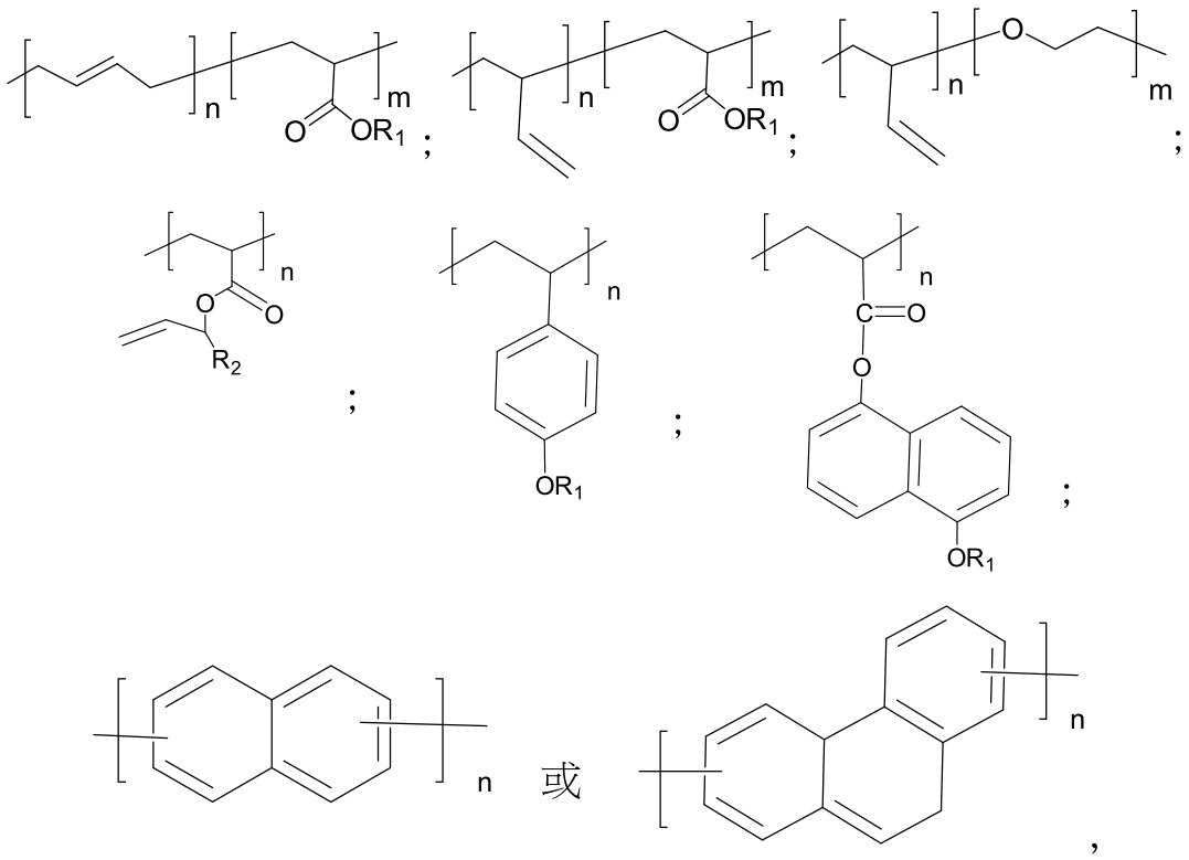
在一些實施例中,富碳聚合物具有以下結構中的一者:

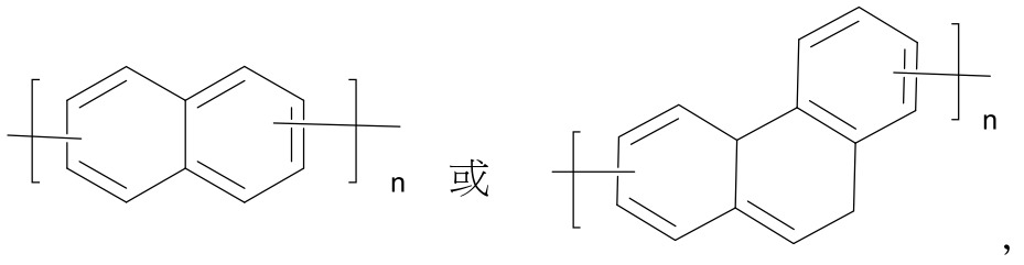
在進一步的實施例中,頂部塗佈層240包含具有上述結構的聚合物的混合物。In a further embodiment, the
在一些實施例中,頂部塗佈層240可包含富矽材料。在一些實施例中,頂部塗佈層240包含富矽聚合物,諸如舉例而言,矽氧烷聚合物(例如,具有-O-Si-O-Si-主鏈的聚合物)。可控制頂部塗佈層材料的矽比率以向頂部塗佈層240提供更高的抗蝕刻性。In some embodiments, the
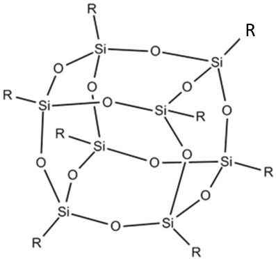
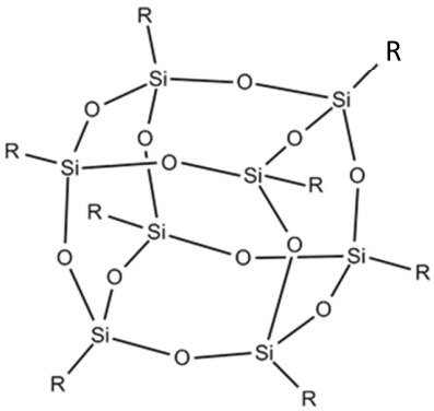
在一些實施例中,頂部塗佈層240包含矽倍半氧烷。舉例而言,頂部塗佈層240可係具有以下結構的籠型矽倍半氧烷:
在一些實施例中,頂部塗佈層240亦可包含與光阻劑層230中的光酸產生劑相同或不同的光酸產生劑。舉例而言,光酸產生劑可係鋶陽離子與磺酸根的鹽類、碘鎓陽離子與磺酸根的鹽類、磺醯基重氮甲烷化合物、N-磺醯氧基醯亞胺光酸產生劑、安息香磺酸鹽光酸產生劑、連苯三酚三磺酸鹽光酸產生劑、硝基苄基磺酸鹽光酸產生劑、碸光酸產生劑、乙二肟衍生物、及三苯基鋶全氟丁基磺酸鹽。光酸產生劑可具有頂部塗佈層240的重量的約1%至30%範圍的濃度。In some embodiments, the
在一些實施例中,頂部塗佈層240進一步包含一或多種添加劑,諸如舉例而言,界面活性劑、淬滅劑、穩定劑、溶解抑制劑、塑化劑、著色劑、附著添加劑、表面調平劑、其組合或類似者。以上關於光阻劑層230描述了各種添加劑的實例,且本文將不進行詳細描述。In some embodiments,
在一些實施例中,頂部塗佈層240可例如藉由旋轉塗佈來沉積。可藉由在光阻劑層230的頂表面上施加包含富碳或富矽材料、光酸產生劑及適合的添加劑及溶劑的頂部塗佈溶液,然後或同時旋轉基板202來實施旋轉塗佈製程,以使頂部塗佈成分分散在光阻劑層230的整個頂表面上。選擇溶劑以不溶解底下的光阻劑層230。在一些實施例中,溶劑係醚型溶劑,諸如舉例而言,乙酸甲酯、乙酸乙酯、乙酸異丙酯、乙酸正丁酯、丙酸乙酯、丁酸正乙酯及乙二醇二乙酸酯、乙二醇單甲醚乙酸酯、乙二醇單乙醚乙酸酯、乙二醇單正丁基醚(丁賽路蘇(butyl cellosolve))或丙二醇單甲醚乙酸酯。在一些實施例中,頂部塗佈層240形成為具有約5 奈米至約10 奈米範圍的厚度。在某些情況下,若頂部塗佈層240的厚度太小,則頂部塗佈層240不能提供足夠的抗蝕刻性以允許將光阻劑圖案完全轉移至中間材料層220中。另一方面,在某些情況下,若頂部塗佈層240的厚度太大,則由於不必要的材料消耗及形成頂部塗佈層240的圖案的處理時間提高,而提高了生產成本。In some embodiments,
隨後,藉由烘烤(即,固化)蒸發紡絲膜中的溶劑以形成頂部塗佈層240。在一些實施例中,烘烤製程可在約攝氏120度至約攝氏350度範圍的溫度下進行。其他烘烤溫度亦適用於蒸發溶劑。Subsequently, the solvent in the spun film is evaporated by baking (ie, curing) to form the
參考第1圖及第2E圖,根據一些實施例,方法100進行至操作110,其中頂部塗佈層240及光阻劑層230曝光於圖案化輻射250。第2E圖係根據一些實施例,將頂部塗佈層240及光阻劑層230曝光於圖案化輻射250之後的第2D圖的半導體結構200的橫截面圖。Referring to FIGS. 1 and 2E , according to some embodiments,
在一些實施例中,頂部塗佈層240及光阻劑層230經由光罩260曝光於來自光源的圖案化輻射250。光罩260具有基於要製造的積體電路的規範而為積體電路設計的預定義圖案。光罩260的圖案對應於構成要被製造的積體電路裝置的各種組件的材料的圖案。舉例而言,積體電路設計佈局的一部分包含各種積體電路特徵,諸如主動區、閘電極、源極及汲極、層間互連結構的金屬線或通孔件及用於接合墊的開口,該些特徵將形成在基板202中及/或置於基板202上的各種材料層中。In some embodiments,
光罩260包含第一區域262及第二區域264。在第一區域262中,圖案化輻射250被光罩260阻擋而不能到達頂部塗佈層240及光阻劑層230,而在第二區域264中,圖案化輻射250未被光罩260阻擋,且可通過光罩260以到達頂部塗佈層240及光阻劑層230。因此,頂部塗佈層240及光阻劑層230在第二區域264之下的部分接收圖案化輻射250,稱為曝光部分。而頂部塗佈層240及光阻劑層230在第一區域262之下的部分不接收圖案化輻射250,稱為未曝光部分。The
在一些實施例中,圖案化輻射250係深紫外(deep ultraviolet,DUV)輻射,諸如氟化氪準分子雷射(248 奈米)或氟化氬準分子雷射(193 奈米)、極紫外線輻射(13.5 奈米)、電子束輻射、x射線輻射、離子束輻射或其他適合的輻射。在一些實施例中,頂部塗佈層240及光阻劑層230以約10 毫焦耳/平方公分(mJ/cm
2)至約60毫焦耳/平方公分的曝光能量曝光於極紫外線輻射束。若曝光能量太高,在某些情況下,圖案化的效率不會改變,但是生產成本提高。若曝光能量太低,則在某些情況下,圖案化的效率太低。在一些實施例中,對於極紫外線微影術及電子束微影術,操作110在液體(浸沒式微影術)或真空中執行。
In some embodiments, patterning
隨後,可對頂部塗佈層240及光阻劑層230進行曝光後烘烤製程。曝光後烘烤製程可在約攝氏50度至約攝氏150度的溫度下進行約60秒至約360秒的執行時間。Subsequently, a post-exposure baking process may be performed on the
參考第1圖及第2F圖,方法100進行至操作112,其中根據一些實施例,使用顯影劑顯影頂部塗佈層240及光阻劑層230以形成經圖案化頂部塗佈層240P及經圖案化光阻劑層230P。第2F圖係根據一些實施例,在形成經圖案化頂部塗佈層240P及經圖案化光阻劑層230P之後的第2E圖的半導體結構200的橫截面圖。Referring to FIGS. 1 and 2F ,
參考第2F圖,在顯影製程期間,將顯影劑施加至頂部塗佈層240及光阻劑層230。取決於抗蝕劑類型,顯影劑可移除頂部塗佈層240及光阻劑層230的曝光或未曝光部分。舉例而言且如第2F圖所示,頂部塗佈層240及光阻劑層230各包含負型光阻劑,因此頂部塗佈層240及光阻劑層230中被圖案化輻射250曝光的部分不被顯影劑溶解且保持在中間材料層220上方。另一方面,若頂部塗佈層240及光阻劑層230各包含正型光阻劑,則頂部塗佈層240及光阻劑層230中被圖案化輻射250曝光的部分將被顯影劑溶解,將未曝光的部分留在中間材料層220上方。Referring to FIG. 2F , during the development process, a developer is applied to the
其餘部分定義了經圖案化頂部塗佈層240P及經圖案化光阻劑層230P中的圖案。圖案含有一或多個開口,在開口中曝光底下的中間材料層220的部分。The remainder defines the patterns in the patterned
顯影劑可包含醇、芳香族烴及類似者。醇的實例包含但不限於甲醇、乙醇、1-丁醇及4-甲基-2-戊醇。芳香族烴的實例包含、但不限於:二甲苯、甲苯及苯。在一些實施例中,顯影劑選自甲醇、4-甲基-2-戊醇及二甲苯中的至少一種。The developer may contain alcohols, aromatic hydrocarbons, and the like. Examples of alcohols include, but are not limited to, methanol, ethanol, 1-butanol, and 4-methyl-2-pentanol. Examples of aromatic hydrocarbons include, but are not limited to: xylene, toluene, and benzene. In some embodiments, the developer is at least one selected from methanol, 4-methyl-2-pentanol and xylene.
可使用任何適合的方法來施加顯影劑。在一些實施例中,藉由將結構浸入顯影劑浴中來施加顯影劑。在一些實施例中,將顯影液噴塗至頂部塗佈層240及光阻劑層230上。The developer can be applied using any suitable method. In some embodiments, the developer is applied by dipping the structure in a developer bath. In some embodiments, a developer solution is sprayed onto the
參考第1圖及第2G圖,方法100進行至操作114,其中根據一些實施例,使用經圖案化頂部塗佈層240P及經圖案化光阻劑層230P作為蝕刻遮罩來蝕刻中間材料層220。第2G圖係根據一些實施例,在使用經圖案化頂部塗佈層240P及經圖案化光阻劑層230P作為蝕刻遮罩蝕刻中間材料層220之後的第2F圖的半導體結構200的橫截面圖。Referring to FIGS. 1 and 2G ,
參考第2G圖,使用經圖案化頂部塗佈層240P及經圖案化光阻劑層230P作為蝕刻遮罩,圖案化中間材料層220,以形成經圖案化中間材料層220P。Referring to FIG. 2G, the
可執行蝕刻製程以將經圖案化頂部塗佈層240P及經圖案化光阻劑層230P中的圖案轉移至中間材料層220。在一些實施例中,所採用的蝕刻製程係非等向性蝕刻,諸如乾式蝕刻,儘管可利用任何適合的蝕刻製程。在一些實施例中,乾式蝕刻係反應性離子蝕刻(reactive ion etch,RIE)或電漿蝕刻。在一些實施例中,乾式蝕刻由含氟氣體(例如,氟甲烷(CF
4)、六氟化硫(SF
6)、二氟甲烷(CH
2F
2)、三氟甲烷(CHF
3)及/或六氟乙烷(C
2F
6)、含氯氣體(例如,氯氣(Cl
2)、三氯甲烷(CHCl
3)、四氯甲烷(CCl
4)及/或三氯化硼(BCl
3)、含溴氣體(例如,溴化氫(HBr)及/或三溴甲烷(CHBr
3)、含氧氣體、含碘氣體、其他適合的氣體及/或電漿或其組合來實施。在一些實施例中,執行氧電漿以蝕刻中間材料層220。在一些實施例中,非等向性蝕刻在約攝氏250度至攝氏450度的溫度下進行約20秒至約300秒的執行時間。
An etching process may be performed to transfer the patterns in the patterned
若在蝕刻製程中未完全消耗,則在形成經圖案化中間材料層220P之後,舉例而言,藉由電漿灰化或濕剝離來移除經圖案化光阻劑層230P。If not completely consumed during the etching process, after forming the patterned
在本揭露中,頂部塗佈層240及光阻劑層230一起用作蝕刻遮罩來蝕刻中間材料層220。由於頂部塗佈層240具有比光阻劑層更高的抗蝕刻性,若假定中間材料層220上的蝕刻時間相同,則光阻劑層230的厚度可形成為小於僅光阻劑層230用作蝕刻遮罩的情況。因此,防止了由於使用厚的光阻劑層而導致的圖案崩壞,而同時確保了光阻劑圖案完全轉移至中間材料層220中。因此,可在中間材料層220中高精度地轉移光阻劑圖案。In the present disclosure, the
參考圖第1圖及第2H圖,方法100進行至操作116,根據一些實施例,其中使用經圖案化中間材料層220P作為蝕刻遮罩來蝕刻底部材料層210。第2H圖係根據一些實施例,在使用經圖案化中間材料層220P作為蝕刻遮罩來蝕刻底部材料層210之後的第2G圖的半導體結構200的橫截面圖。Referring to FIGS. 1 and 2H ,
參考第2H圖,使用經圖案化中間材料層220P作為蝕刻遮罩來蝕刻底部材料層210,以形成經圖案化底部材料層210P。底部材料層210的蝕刻曝光了底下的基板202的部分。Referring to FIG. 2H, the
可執行蝕刻製程以將經圖案化中間材料層220P中的圖案轉移至底部材料層210。在一些實施例中,蝕刻製程係非等向性蝕刻,諸如乾式蝕刻。在一些實施例中,乾式蝕刻係反應性離子蝕刻或電漿蝕刻。An etching process may be performed to transfer the pattern in the patterned
參考第1圖及第2I圖,方法100進行至操作118,根據一些實施例,其中使用經圖案化中間材料層220P及經圖案化底部材料層210P作為蝕刻遮罩來蝕刻基板202的上部部分。第2I圖係根據一些實施例,使用經圖案化中間材料層220P及經圖案化底部材料層210P作為蝕刻遮罩來蝕刻基板202的上部部分之後的第2H圖的半導體結構200的橫截面圖。Referring to FIGS. 1 and 21 ,
參考第2I圖,使用經圖案化中間材料層220P及經圖案化底部材料層210P作為蝕刻遮罩來蝕刻基板202,以在基板202中形成經圖案化特徵202P。經圖案化特徵202P可係閘極結構、諸如在鰭式場效電晶體中提供的鰭結構、互連結構、隔離特徵、諸如接線的導電特徵、及/或其他適合的半導體裝置特徵。Referring to FIG. 21 , the
可執行蝕刻製程以移除基板202中被經圖案化中間材料層220P及經圖案化底部材料層210P暴露的部分。在一些實施例中,蝕刻製程係非等向性蝕刻,諸如乾式蝕刻。在一些實施例中,乾式蝕刻係反應性離子蝕刻或電漿蝕刻。An etching process may be performed to remove portions of the
本說明書的一個態樣涉及圖案化堆疊。圖案化堆疊包含基板上方的底部抗反射塗佈(bottom anti-reflective coating,BARC)層、在底部抗反射塗佈層上方的具有第一抗蝕刻性的光阻劑層、及在光阻劑層上方的具有大於第一抗蝕刻性的第二抗蝕刻性的頂部塗佈層。頂部塗佈層包含具有聚合物主鏈的聚合物,聚合物主鏈包含具有高抗蝕刻性的至少一個功能單元及連接至聚合物主鏈或矽籠化合物的一或多個酸不穩定基團。One aspect of the description relates to patterned stacking. The patterned stack includes a bottom anti-reflective coating (BARC) layer over the substrate, a photoresist layer having a first etch resistance over the bottom anti-reflective coating layer, and a photoresist layer over the photoresist layer. An overlying top coating layer having a second etch resistance greater than the first etch resistance. The top coating layer comprises a polymer having a polymer backbone comprising at least one functional unit having high etch resistance and one or more acid-labile groups attached to the polymer backbone or a silicon cage compound .
在一些實施例中,至少一個高抗蝕刻性的功能單元選自由三級碳、雙鍵、三鍵及芳香族基團組成的群組。In some embodiments, at least one functional unit with high etch resistance is selected from the group consisting of tertiary carbons, double bonds, triple bonds and aromatic groups.
在一些實施例中,一或多個酸不穩定基團包含羧酸、氟化醇、酚醇、磺基、磺醯胺、磺醯亞胺基、(烷基磺醯基)亞甲基、(烷基羰基)亞甲基、(烷基磺醯基)醯亞胺基、(烷基羰基)醯亞胺基、雙(烷基羰基)亞甲基、雙(烷基羰基)醯亞胺基、雙(烷基磺醯基)亞甲基、雙(烷基磺醯基)醯亞胺基、三(烷基羰基)醯亞胺基或三(烷基磺醯基)亞甲基。In some embodiments, the one or more acid labile groups comprise carboxylic acid, fluorinated alcohol, phenolic alcohol, sulfo, sulfonamide, sulfonimide, (alkylsulfonyl)methylene, (Alkylcarbonyl)methylene, (Alkylsulfonyl)imide, (Alkylcarbonyl)imide, bis(alkylcarbonyl)methylene, bis(alkylcarbonyl)imide group, bis(alkylsulfonyl)methylene group, bis(alkylsulfonyl)imide group, tris(alkylcarbonyl)imide group or tris(alkylsulfonyl)methylene group.
在一些實施例中,頂部塗佈層更包含光酸產生劑。In some embodiments, the top coating layer further includes a photoacid generator.
在一些實施例中,頂部塗佈層更包含淬滅劑。In some embodiments, the top coating layer further includes a quencher.
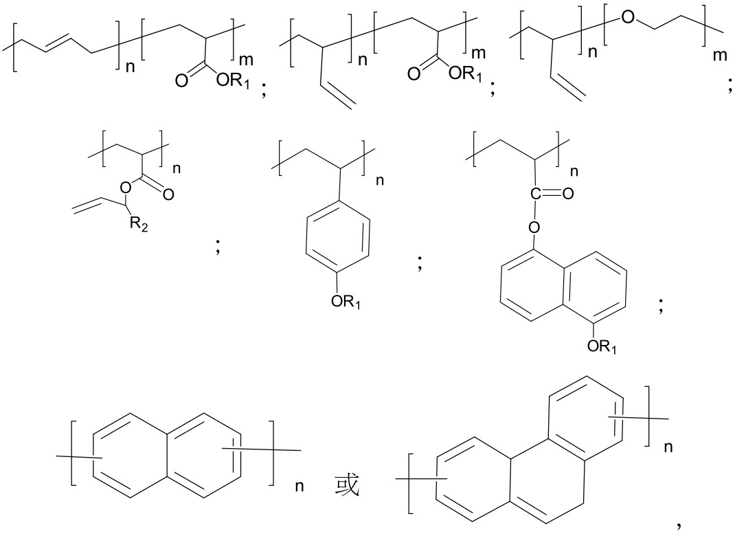
在一些實施例中,頂部塗佈層包含具有以下結構中的一者的聚合物:
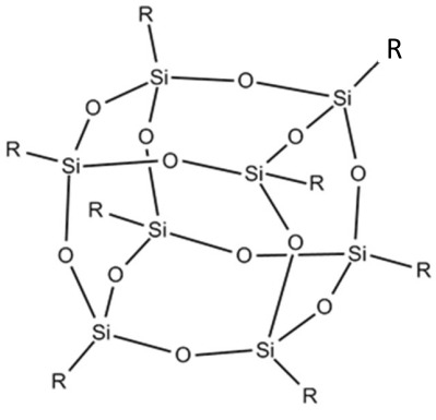
在一些實施例中,矽籠化合物係具有以下結構的矽倍半氧烷:
在一些實施例中,圖案化堆疊更包含在底部抗反射塗佈層與基板之間的平坦化層。In some embodiments, the patterned stack further includes a planarization layer between the BARC layer and the substrate.
在一些實施例中,底部抗反射塗佈層包含氧化矽或碳化矽氧。In some embodiments, the BARC layer includes silicon oxide or silicon carbide oxide.
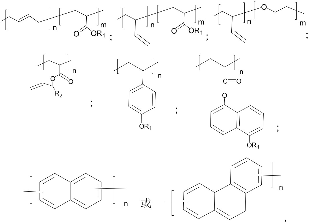
本說明書的另一態樣涉及圖案化堆疊。圖案化堆疊包含在基板上方的第一材料層、在第一材料層上方的第二材料層、在第二材料層上方具有第一抗蝕刻性的光阻劑層、及在光阻劑層上方具有大於第一抗蝕刻性的第二抗蝕刻性的頂部塗佈層。頂部塗佈層包含聚合物、光酸產生劑及淬滅劑,聚合物具有以下結構中的一者:
在一些實施例中,酸不穩定基團包含羧酸、氟化醇、酚醇、磺基、磺醯胺、磺醯亞胺基、(烷基磺醯基)亞甲基、(烷基羰基)亞甲基、(烷基磺醯基)醯亞胺基、(烷基羰基)醯亞胺基、雙(烷基羰基)亞甲基、雙(烷基羰基)醯亞胺基、雙(烷基磺醯基)亞甲基、雙(烷基磺醯基)醯亞胺基、三(烷基羰基)醯亞胺基或三(烷基磺醯基)亞甲基。In some embodiments, the acid labile group comprises carboxylic acid, fluorinated alcohol, phenolic alcohol, sulfo, sulfonamide, sulfonimide, (alkylsulfonyl)methylene, (alkylcarbonyl ) methylene, (alkylsulfonyl) imide, (alkylcarbonyl) imide, bis (alkylcarbonyl) methylene, bis (alkylcarbonyl) imide, bis ( Alkylsulfonyl)methylene, bis(alkylsulfonyl)imide, tris(alkylcarbonyl)imide or tris(alkylsulfonyl)methylene.
在一些實施例中,第一材料層包含旋轉塗佈的碳、類鑽碳、聚亞芳香醚或聚醯亞胺。In some embodiments, the first material layer includes spin-on carbon, diamond-like carbon, polyarylene ether, or polyimide.
在一些實施例中,第二材料層包含聚合物,該聚合物具有聚合物主鏈及連接至聚合物主鏈的一或多個交聯劑基團、一或多個發色團及一或多個極性基團。In some embodiments, the second material layer comprises a polymer having a polymer backbone and one or more crosslinker groups attached to the polymer backbone, one or more chromophores, and one or more multiple polar groups.
在一些實施例中,聚合物具有至少80%的碳含量。In some embodiments, the polymer has a carbon content of at least 80%.
在一些實施例中,頂部塗佈層具有約5奈米至約10奈米範圍的厚度。In some embodiments, the top coating layer has a thickness ranging from about 5 nanometers to about 10 nanometers.
本說明書的又一態樣涉及形成半導體結構的方法。方法包含在基板上方沉積第一材料層;在第一材料層上方沉積第二材料層;在第二材料層上方形成具有第一抗蝕刻性的光阻劑層;在光阻劑層上方形成具有大於第一抗蝕刻性的第二抗蝕刻性的頂部塗佈層;圖案化頂部塗佈層及光阻劑層以提供經圖案化頂部塗佈層及經圖案化光阻劑層;及使用經圖案化頂部塗佈層及經圖案化光阻劑層作為蝕刻遮罩來蝕刻第二材料層以提供經圖案化第二材料層。頂部塗佈層包含具有聚合物主鏈的聚合物,聚合物主鏈含有具有高抗蝕刻性的至少一個功能單元及連接至聚合物主鏈或矽籠化合物的一或多個酸不穩定基團。Yet another aspect of the specification relates to a method of forming a semiconductor structure. The method includes depositing a first material layer over a substrate; depositing a second material layer over the first material layer; forming a photoresist layer having first etch resistance over the second material layer; forming a photoresist layer over the photoresist layer a top coating layer having a second etch resistance greater than the first etch resistance; patterning the top coating layer and the photoresist layer to provide a patterned top coating layer and a patterned photoresist layer; The patterned top coating layer and the patterned photoresist layer serve as an etch mask to etch the second material layer to provide a patterned second material layer. The top coating layer comprises a polymer having a polymer backbone containing at least one functional unit having high etch resistance and one or more acid-labile groups attached to the polymer backbone or a silicon cage compound .
在一些實施例中,圖案化頂部塗佈層及光阻劑層包含將頂部塗佈層及光阻劑層曝光於輻射。In some embodiments, patterning the top coating layer and the photoresist layer includes exposing the top coating layer and the photoresist layer to radiation.
在一些實施例中,輻射係極紫外輻射。In some embodiments, the radiation is extreme ultraviolet radiation.
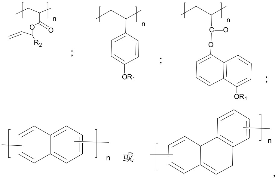
在一些實施例中,聚合物具有以下結構中的一者:

矽籠化合物具有以下結構:
前述內容概述幾個實施例的特徵,使得熟習此項技術者可更佳地理解本揭露的態樣。熟習此項技術者應瞭解,該些技術者可容易將本揭露用作作為設計或修改用於實現本文中介紹的實施例的相同目的及/或達成與本文中介紹的實施例的相同優優點的其他製程及結構的基礎。熟習此項技術者亦應認識至,此等等效構造不背離本揭露的精神及範疇,且該些技術者可在不背離本揭露的精神及範疇的情況下作出本文中的各種改變、取代及改動。The foregoing summary outlines features of several embodiments so that those skilled in the art may better understand aspects of the present disclosure. Those skilled in the art should appreciate that those skilled in the art can readily use the present disclosure as a design or modification for achieving the same purpose and/or achieving the same advantages as the embodiments described herein. The basis of other processes and structures. Those skilled in the art should also realize that such equivalent structures do not depart from the spirit and scope of the present disclosure, and those skilled in the art can make various changes and substitutions herein without departing from the spirit and scope of the present disclosure. and changes.
100:方法
102:操作
104:操作
106:操作
108:操作
110:操作
112:操作
114:操作
116:操作
118:操作
200:半導體結構
202:基板
202P:經圖案化特徵
210:底部材料層
210P:經圖案化底部材料層
220:中間材料層
220P:經圖案化中間材料層
230:光阻劑層
230P:經圖案化光阻劑層
240:頂部塗佈層
240P:經圖案化頂部塗佈層
250:圖案化輻射
260:光罩
262:第一區域
264:第二區域
310:聚合物
312:聚合物主鏈
314:第一側基
316:第二側基
318:第三側基
320:添加劑
100: method
102: Operation
104: Operation
106: Operation
108: Operation
110: Operation
112: Operation
114: Operation
116: Operation
118: Operation
200: Semiconductor Structures
202:
本揭露的態樣將在結合附圖閱讀時自以下詳細描述最佳地瞭解。應注意,根據行業中的標準慣例,各種特徵未按比例繪製。實際上,各種特徵的尺寸可為了論述清楚經任意地增大或減小。 第1圖係根據一些實施例的用於製造半導體結構的方法的流程圖。 第2A圖至第2I圖係根據一些實施例的使用第1圖的方法製造的半導體結構的橫截面圖。 第3圖圖示根據一些實施例的可在中間材料層中使用的組成物。 Aspects of the present disclosure are best understood from the following detailed description when read in conjunction with the accompanying drawings. It should be noted that, in accordance with the standard practice in the industry, various features are not drawn to scale. In fact, the dimensions of the various features may be arbitrarily increased or decreased for clarity of discussion. FIG. 1 is a flowchart of a method for fabricating a semiconductor structure in accordance with some embodiments. FIGS. 2A-21 are cross-sectional views of semiconductor structures fabricated using the method of FIG. 1 , according to some embodiments. Figure 3 illustrates compositions that may be used in the intermediate material layer according to some embodiments.
國內寄存資訊(請依寄存機構、日期、號碼順序註記) 無 國外寄存資訊(請依寄存國家、機構、日期、號碼順序註記) 無 Domestic deposit information (please note in order of depositor, date, and number) none Overseas storage information (please note in order of storage country, institution, date, and number) none
310:聚合物 310: polymer
312:聚合物主鏈 312: Polymer backbone
314:第一側基 314: First side base
316:第二側基 316:Second side base
318:第三側基 318: The third side base
320:添加劑 320: Additives
Claims (20)




Applications Claiming Priority (2)
| Application Number | Priority Date | Filing Date | Title |
|---|---|---|---|
| US17/231,946 | 2021-04-15 | ||
| US17/231,946 US12535738B2 (en) | 2021-04-15 | 2021-04-15 | Photoresist top coating material for etching rate control |
Publications (1)
| Publication Number | Publication Date |
|---|---|
| TW202242547A true TW202242547A (en) | 2022-11-01 |
Family
ID=82764166
Family Applications (1)
| Application Number | Title | Priority Date | Filing Date |
|---|---|---|---|
| TW111106651A TW202242547A (en) | 2021-04-15 | 2022-02-23 | Patterning stack |
Country Status (3)
| Country | Link |
|---|---|
| US (2) | US12535738B2 (en) |
| CN (1) | CN114911133A (en) |
| TW (1) | TW202242547A (en) |
Families Citing this family (1)
| Publication number | Priority date | Publication date | Assignee | Title |
|---|---|---|---|---|
| KR20240026997A (en) * | 2021-06-24 | 2024-02-29 | 도쿄엘렉트론가부시키가이샤 | Substrate processing method and substrate processing system |
Family Cites Families (24)
| Publication number | Priority date | Publication date | Assignee | Title |
|---|---|---|---|---|
| JPH085927B2 (en) * | 1986-12-26 | 1996-01-24 | 日本合成ゴム株式会社 | Photosensitive resin composition |
| US5145764A (en) * | 1990-04-10 | 1992-09-08 | E. I. Du Pont De Nemours And Company | Positive working resist compositions process of exposing, stripping developing |
| JP3575109B2 (en) * | 1995-05-10 | 2004-10-13 | Jsr株式会社 | Bump forming material |
| US6117967A (en) * | 1999-06-04 | 2000-09-12 | Xerox Corporation | Arylene ether alcohol polymers |
| US6737222B2 (en) * | 2000-11-21 | 2004-05-18 | Advanced Micro Devices, Inc. | Dual damascene process utilizing a bi-layer imaging layer |
| US7361607B2 (en) * | 2003-06-27 | 2008-04-22 | Lam Research Corporation | Method for multi-layer resist plasma etch |
| KR100586165B1 (en) * | 2003-12-30 | 2006-06-07 | 동부일렉트로닉스 주식회사 | Floor anti-reflective coating method |
| EP1612604A3 (en) * | 2004-07-02 | 2006-04-05 | Rohm and Haas Electronic Materials, L.L.C. | Compositions and processes for immersion lithography |
| US7387969B2 (en) * | 2005-03-18 | 2008-06-17 | Taiwan Semiconductor Manufacturing Co., Ltd. | Top patterned hardmask and method for patterning |
| US20070196773A1 (en) * | 2006-02-22 | 2007-08-23 | Weigel Scott J | Top coat for lithography processes |
| US7435537B2 (en) | 2006-06-21 | 2008-10-14 | International Business Machines Corporation | Fluorinated half ester of maleic anhydride polymers for dry 193 nm top antireflective coating application |
| WO2009072465A1 (en) * | 2007-12-07 | 2009-06-11 | Mitsubishi Gas Chemical Company, Inc. | Composition for forming base film for lithography and method for forming multilayer resist pattern |
| US20090174036A1 (en) | 2008-01-04 | 2009-07-09 | International Business Machines Corporation | Plasma curing of patterning materials for aggressively scaled features |
| US8084193B2 (en) * | 2008-07-12 | 2011-12-27 | International Business Machines Corporation | Self-segregating multilayer imaging stack with built-in antireflective properties |
| US20120122029A1 (en) * | 2010-11-11 | 2012-05-17 | Takanori Kudo | Underlayer Developable Coating Compositions and Processes Thereof |
| US8623589B2 (en) * | 2011-06-06 | 2014-01-07 | Az Electronic Materials Usa Corp. | Bottom antireflective coating compositions and processes thereof |
| JP6119667B2 (en) * | 2013-06-11 | 2017-04-26 | 信越化学工業株式会社 | Underlayer film material and pattern forming method |
| JP6267532B2 (en) * | 2014-02-14 | 2018-01-24 | 信越化学工業株式会社 | Resist protective film material and pattern forming method |
| JP5882510B2 (en) * | 2014-06-30 | 2016-03-09 | 太陽インキ製造株式会社 | Photosensitive dry film and method for producing printed wiring board using the same |
| US9595441B2 (en) * | 2014-12-22 | 2017-03-14 | Tokyo Electron Limited | Patterning a substrate using grafting polymer material |
| US9917189B2 (en) * | 2015-07-31 | 2018-03-13 | Taiwan Semiconductor Manufacturing Company, Ltd. | Method for detecting presence and location of defects in a substrate |
| US10312075B2 (en) * | 2015-09-30 | 2019-06-04 | Taiwan Semiconductor Manufacturing Company, Ltd. | Treatment system and method |
| US9983475B2 (en) | 2016-08-12 | 2018-05-29 | International Business Machines Corporation | Fluorinated sulfonate esters of aryl ketones for non-ionic photo-acid generators |
| US10347486B1 (en) * | 2017-12-19 | 2019-07-09 | International Business Machines Corporation | Patterning material film stack with metal-containing top coat for enhanced sensitivity in extreme ultraviolet (EUV) lithography |
-
2021
- 2021-04-15 US US17/231,946 patent/US12535738B2/en active Active
-
2022
- 2022-02-23 TW TW111106651A patent/TW202242547A/en unknown
- 2022-04-12 CN CN202210382238.XA patent/CN114911133A/en active Pending
-
2023
- 2023-08-10 US US18/447,673 patent/US12607937B2/en active Active
Also Published As
| Publication number | Publication date |
|---|---|
| US20240192601A1 (en) | 2024-06-13 |
| US12535738B2 (en) | 2026-01-27 |
| US20220334482A1 (en) | 2022-10-20 |
| CN114911133A (en) | 2022-08-16 |
| US12607937B2 (en) | 2026-04-21 |
Similar Documents
| Publication | Publication Date | Title |
|---|---|---|
| US20240377731A1 (en) | Extreme ultraviolet photolithography method with developer composition | |
| KR102708968B1 (en) | Protective composition and method of forming photoresist pattern | |
| CN107068542B (en) | Method for manufacturing semiconductor device | |
| US8623739B2 (en) | Method of manufacturing semiconductor device using acid diffusion | |
| US20180315617A1 (en) | Material composition and methods thereof | |
| US10672619B2 (en) | Material composition and methods thereof | |
| US12607937B2 (en) | Photoresist top coating material for etching rate control | |
| CN113314402A (en) | Photoresist composition and method for manufacturing semiconductor device | |
| US12476107B2 (en) | Method of manufacturing a semiconductor device | |
| TWI829545B (en) | Method of forming semiconductor structure | |
| TW201913730A (en) | Method of performing lithography process | |
| TWI914837B (en) | Method for forming semiconductor device and photoresist composition | |
| US12374639B2 (en) | Non-DMSO stripper for advance package metal plating process | |
| US12106961B2 (en) | Humidity control or aqueous treatment for EUV metallic resist | |
| TWI863423B (en) | Method of manufacturing a semiconductor device and photoresist composition | |
| US20240210822A1 (en) | Switchable substrate for extreme ultraviolet or e-beam metallic resist | |
| TW202528377A (en) | Photoresist compositions | |
| TW202445267A (en) | Method of forming semiconductor device | |
| CN117826534A (en) | Method for forming a semiconductor device | |
| TW202345286A (en) | Method of forming semiconductor device | |
| CN115202155A (en) | Method for reducing photoresist consumption and method for forming semiconductor structure |