TWI667360B - Organic electroluminescent device and preparation method thereof - Google Patents
Organic electroluminescent device and preparation method thereof Download PDFInfo
- Publication number
- TWI667360B TWI667360B TW107101972A TW107101972A TWI667360B TW I667360 B TWI667360 B TW I667360B TW 107101972 A TW107101972 A TW 107101972A TW 107101972 A TW107101972 A TW 107101972A TW I667360 B TWI667360 B TW I667360B
- Authority
- TW
- Taiwan
- Prior art keywords
- ring
- host material
- organic electroluminescent
- electroluminescent device
- host
- Prior art date
Links
- 238000002360 preparation method Methods 0.000 title description 4
- 239000000463 material Substances 0.000 claims abstract description 131
- 238000001704 evaporation Methods 0.000 claims abstract description 26
- 230000008020 evaporation Effects 0.000 claims abstract description 26
- 238000000034 method Methods 0.000 claims abstract description 16
- 238000010549 co-Evaporation Methods 0.000 claims abstract description 8
- 238000002347 injection Methods 0.000 claims description 20
- 239000007924 injection Substances 0.000 claims description 20
- 230000003287 optical effect Effects 0.000 claims description 19
- 125000000623 heterocyclic group Chemical group 0.000 claims description 16
- 230000005540 biological transmission Effects 0.000 claims description 12
- -1 (9-fluorenyl)- Chemical class 0.000 claims description 11
- 230000000903 blocking effect Effects 0.000 claims description 11
- 150000001875 compounds Chemical class 0.000 claims description 8
- 230000005525 hole transport Effects 0.000 claims description 8
- 239000000758 substrate Substances 0.000 claims description 8
- 229910052757 nitrogen Inorganic materials 0.000 claims description 7
- 125000001997 phenyl group Chemical group [H]C1=C([H])C([H])=C(*)C([H])=C1[H] 0.000 claims description 7
- 238000004770 highest occupied molecular orbital Methods 0.000 claims description 6
- 125000001624 naphthyl group Chemical group 0.000 claims description 6
- 125000004433 nitrogen atom Chemical group N* 0.000 claims description 6
- 238000004768 lowest unoccupied molecular orbital Methods 0.000 claims description 5
- 125000000732 arylene group Chemical group 0.000 claims description 4
- 125000004429 atom Chemical group 0.000 claims description 4
- 125000005549 heteroarylene group Chemical group 0.000 claims description 4
- 125000001424 substituent group Chemical group 0.000 claims description 4
- 150000001454 anthracenes Chemical group 0.000 claims description 3
- 230000009477 glass transition Effects 0.000 claims description 3
- 125000005577 anthracene group Chemical group 0.000 claims description 2
- 238000006467 substitution reaction Methods 0.000 claims description 2
- 230000008021 deposition Effects 0.000 claims 1
- QJGQUHMNIGDVPM-UHFFFAOYSA-N nitrogen group Chemical group [N] QJGQUHMNIGDVPM-UHFFFAOYSA-N 0.000 claims 1
- 238000005401 electroluminescence Methods 0.000 abstract description 14
- 230000008569 process Effects 0.000 abstract description 6
- 230000005284 excitation Effects 0.000 description 7
- 239000000969 carrier Substances 0.000 description 6
- 238000004519 manufacturing process Methods 0.000 description 6
- 125000005842 heteroatom Chemical group 0.000 description 5
- YERGTYJYQCLVDM-UHFFFAOYSA-N iridium(3+);2-(4-methylphenyl)pyridine Chemical compound [Ir+3].C1=CC(C)=CC=C1C1=CC=CC=N1.C1=CC(C)=CC=C1C1=CC=CC=N1.C1=CC(C)=CC=C1C1=CC=CC=N1 YERGTYJYQCLVDM-UHFFFAOYSA-N 0.000 description 5
- 239000000126 substance Substances 0.000 description 5
- 230000000052 comparative effect Effects 0.000 description 4
- 230000003111 delayed effect Effects 0.000 description 4
- PQXKHYXIUOZZFA-UHFFFAOYSA-M lithium fluoride Chemical compound [Li+].[F-] PQXKHYXIUOZZFA-UHFFFAOYSA-M 0.000 description 4
- 239000011777 magnesium Substances 0.000 description 4
- 229910052751 metal Inorganic materials 0.000 description 4
- 239000002184 metal Substances 0.000 description 4
- 239000002243 precursor Substances 0.000 description 4
- UHOVQNZJYSORNB-UHFFFAOYSA-N Benzene Chemical compound C1=CC=CC=C1 UHOVQNZJYSORNB-UHFFFAOYSA-N 0.000 description 3
- WHXSMMKQMYFTQS-UHFFFAOYSA-N Lithium Chemical compound [Li] WHXSMMKQMYFTQS-UHFFFAOYSA-N 0.000 description 3
- 238000010586 diagram Methods 0.000 description 3
- 229910052744 lithium Inorganic materials 0.000 description 3
- 238000011112 process operation Methods 0.000 description 3
- 230000006798 recombination Effects 0.000 description 3
- 238000005215 recombination Methods 0.000 description 3
- IJGRMHOSHXDMSA-UHFFFAOYSA-N Atomic nitrogen Chemical compound N#N IJGRMHOSHXDMSA-UHFFFAOYSA-N 0.000 description 2
- OYPRJOBELJOOCE-UHFFFAOYSA-N Calcium Chemical compound [Ca] OYPRJOBELJOOCE-UHFFFAOYSA-N 0.000 description 2
- RYGMFSIKBFXOCR-UHFFFAOYSA-N Copper Chemical compound [Cu] RYGMFSIKBFXOCR-UHFFFAOYSA-N 0.000 description 2
- SMWDFEZZVXVKRB-UHFFFAOYSA-N Quinoline Chemical compound N1=CC=CC2=CC=CC=C21 SMWDFEZZVXVKRB-UHFFFAOYSA-N 0.000 description 2
- BQCADISMDOOEFD-UHFFFAOYSA-N Silver Chemical compound [Ag] BQCADISMDOOEFD-UHFFFAOYSA-N 0.000 description 2
- XLOMVQKBTHCTTD-UHFFFAOYSA-N Zinc monoxide Chemical compound [Zn]=O XLOMVQKBTHCTTD-UHFFFAOYSA-N 0.000 description 2
- MCMNRKCIXSYSNV-UHFFFAOYSA-N Zirconium dioxide Chemical compound O=[Zr]=O MCMNRKCIXSYSNV-UHFFFAOYSA-N 0.000 description 2
- 239000000956 alloy Substances 0.000 description 2
- 229910045601 alloy Inorganic materials 0.000 description 2
- 229910052782 aluminium Inorganic materials 0.000 description 2
- 125000000319 biphenyl-4-yl group Chemical group [H]C1=C([H])C([H])=C([H])C([H])=C1C1=C([H])C([H])=C([*])C([H])=C1[H] 0.000 description 2
- UFVXQDWNSAGPHN-UHFFFAOYSA-K bis[(2-methylquinolin-8-yl)oxy]-(4-phenylphenoxy)alumane Chemical compound [Al+3].C1=CC=C([O-])C2=NC(C)=CC=C21.C1=CC=C([O-])C2=NC(C)=CC=C21.C1=CC([O-])=CC=C1C1=CC=CC=C1 UFVXQDWNSAGPHN-UHFFFAOYSA-K 0.000 description 2
- XJHCXCQVJFPJIK-UHFFFAOYSA-M caesium fluoride Chemical compound [F-].[Cs+] XJHCXCQVJFPJIK-UHFFFAOYSA-M 0.000 description 2
- 229910052791 calcium Inorganic materials 0.000 description 2
- 239000011575 calcium Substances 0.000 description 2
- 229920001940 conductive polymer Polymers 0.000 description 2
- 229910052802 copper Inorganic materials 0.000 description 2
- 239000010949 copper Substances 0.000 description 2
- 230000009849 deactivation Effects 0.000 description 2
- ZUOUZKKEUPVFJK-UHFFFAOYSA-N diphenyl Chemical compound C1=CC=CC=C1C1=CC=CC=C1 ZUOUZKKEUPVFJK-UHFFFAOYSA-N 0.000 description 2
- 230000009977 dual effect Effects 0.000 description 2
- 238000002866 fluorescence resonance energy transfer Methods 0.000 description 2
- PCHJSUWPFVWCPO-UHFFFAOYSA-N gold Chemical compound [Au] PCHJSUWPFVWCPO-UHFFFAOYSA-N 0.000 description 2
- 229910052737 gold Inorganic materials 0.000 description 2
- 239000010931 gold Substances 0.000 description 2
- AMWRITDGCCNYAT-UHFFFAOYSA-L hydroxy(oxo)manganese;manganese Chemical compound [Mn].O[Mn]=O.O[Mn]=O AMWRITDGCCNYAT-UHFFFAOYSA-L 0.000 description 2
- 229910010272 inorganic material Inorganic materials 0.000 description 2
- 239000011147 inorganic material Substances 0.000 description 2
- 229910052749 magnesium Inorganic materials 0.000 description 2
- 229910044991 metal oxide Inorganic materials 0.000 description 2
- 150000004706 metal oxides Chemical class 0.000 description 2
- 150000002790 naphthalenes Chemical group 0.000 description 2
- 230000003647 oxidation Effects 0.000 description 2
- 238000007254 oxidation reaction Methods 0.000 description 2
- IEQIEDJGQAUEQZ-UHFFFAOYSA-N phthalocyanine Chemical class N1C(N=C2C3=CC=CC=C3C(N=C3C4=CC=CC=C4C(=N4)N3)=N2)=C(C=CC=C2)C2=C1N=C1C2=CC=CC=C2C4=N1 IEQIEDJGQAUEQZ-UHFFFAOYSA-N 0.000 description 2
- 229920000767 polyaniline Polymers 0.000 description 2
- AHLATJUETSFVIM-UHFFFAOYSA-M rubidium fluoride Chemical compound [F-].[Rb+] AHLATJUETSFVIM-UHFFFAOYSA-M 0.000 description 2
- 229910052709 silver Inorganic materials 0.000 description 2
- 239000004332 silver Substances 0.000 description 2
- NDVLTYZPCACLMA-UHFFFAOYSA-N silver oxide Chemical compound [O-2].[Ag+].[Ag+] NDVLTYZPCACLMA-UHFFFAOYSA-N 0.000 description 2
- 229910052717 sulfur Inorganic materials 0.000 description 2
- IWZZBBJTIUYDPZ-DVACKJPTSA-N (z)-4-hydroxypent-3-en-2-one;iridium;2-phenylpyridine Chemical compound [Ir].C\C(O)=C\C(C)=O.[C-]1=CC=CC=C1C1=CC=CC=N1.[C-]1=CC=CC=C1C1=CC=CC=N1 IWZZBBJTIUYDPZ-DVACKJPTSA-N 0.000 description 1
- XANIFASCQKHXRC-UHFFFAOYSA-N 2-(1,3-benzothiazol-2-yl)phenol zinc Chemical compound [Zn].Oc1ccccc1-c1nc2ccccc2s1.Oc1ccccc1-c1nc2ccccc2s1 XANIFASCQKHXRC-UHFFFAOYSA-N 0.000 description 1
- UOCMXZLNHQBBOS-UHFFFAOYSA-N 2-(1,3-benzoxazol-2-yl)phenol zinc Chemical compound [Zn].Oc1ccccc1-c1nc2ccccc2o1.Oc1ccccc1-c1nc2ccccc2o1 UOCMXZLNHQBBOS-UHFFFAOYSA-N 0.000 description 1
- FQJQNLKWTRGIEB-UHFFFAOYSA-N 2-(4-tert-butylphenyl)-5-[3-[5-(4-tert-butylphenyl)-1,3,4-oxadiazol-2-yl]phenyl]-1,3,4-oxadiazole Chemical compound C1=CC(C(C)(C)C)=CC=C1C1=NN=C(C=2C=C(C=CC=2)C=2OC(=NN=2)C=2C=CC(=CC=2)C(C)(C)C)O1 FQJQNLKWTRGIEB-UHFFFAOYSA-N 0.000 description 1
- NSMJMUQZRGZMQC-UHFFFAOYSA-N 2-naphthalen-1-yl-1H-imidazo[4,5-f][1,10]phenanthroline Chemical compound C12=CC=CN=C2C2=NC=CC=C2C2=C1NC(C=1C3=CC=CC=C3C=CC=1)=N2 NSMJMUQZRGZMQC-UHFFFAOYSA-N 0.000 description 1
- DHDHJYNTEFLIHY-UHFFFAOYSA-N 4,7-diphenyl-1,10-phenanthroline Chemical compound C1=CC=CC=C1C1=CC=NC2=C1C=CC1=C(C=3C=CC=CC=3)C=CN=C21 DHDHJYNTEFLIHY-UHFFFAOYSA-N 0.000 description 1
- AWXGSYPUMWKTBR-UHFFFAOYSA-N 4-carbazol-9-yl-n,n-bis(4-carbazol-9-ylphenyl)aniline Chemical compound C12=CC=CC=C2C2=CC=CC=C2N1C1=CC=C(N(C=2C=CC(=CC=2)N2C3=CC=CC=C3C3=CC=CC=C32)C=2C=CC(=CC=2)N2C3=CC=CC=C3C3=CC=CC=C32)C=C1 AWXGSYPUMWKTBR-UHFFFAOYSA-N 0.000 description 1
- 125000004860 4-ethylphenyl group Chemical group [H]C1=C([H])C(=C([H])C([H])=C1*)C([H])([H])C([H])([H])[H] 0.000 description 1
- 229910001316 Ag alloy Inorganic materials 0.000 description 1
- JPVYNHNXODAKFH-UHFFFAOYSA-N Cu2+ Chemical compound [Cu+2] JPVYNHNXODAKFH-UHFFFAOYSA-N 0.000 description 1
- 101000837344 Homo sapiens T-cell leukemia translocation-altered gene protein Proteins 0.000 description 1
- FYYHWMGAXLPEAU-UHFFFAOYSA-N Magnesium Chemical compound [Mg] FYYHWMGAXLPEAU-UHFFFAOYSA-N 0.000 description 1
- VUMVABVDHWICAZ-UHFFFAOYSA-N N-phenyl-N-[4-[4-[N-(9,9'-spirobi[fluorene]-2-yl)anilino]phenyl]phenyl]-9,9'-spirobi[fluorene]-2-amine Chemical group C1=CC=CC=C1N(C=1C=C2C3(C4=CC=CC=C4C4=CC=CC=C43)C3=CC=CC=C3C2=CC=1)C1=CC=C(C=2C=CC(=CC=2)N(C=2C=CC=CC=2)C=2C=C3C4(C5=CC=CC=C5C5=CC=CC=C54)C4=CC=CC=C4C3=CC=2)C=C1 VUMVABVDHWICAZ-UHFFFAOYSA-N 0.000 description 1
- 229920000144 PEDOT:PSS Polymers 0.000 description 1
- 239000004642 Polyimide Substances 0.000 description 1
- BUGBHKTXTAQXES-UHFFFAOYSA-N Selenium Chemical group [Se] BUGBHKTXTAQXES-UHFFFAOYSA-N 0.000 description 1
- NINIDFKCEFEMDL-UHFFFAOYSA-N Sulfur Chemical compound [S] NINIDFKCEFEMDL-UHFFFAOYSA-N 0.000 description 1
- 102100028692 T-cell leukemia translocation-altered gene protein Human genes 0.000 description 1
- GWEVSGVZZGPLCZ-UHFFFAOYSA-N Titan oxide Chemical compound O=[Ti]=O GWEVSGVZZGPLCZ-UHFFFAOYSA-N 0.000 description 1
- WGLPBDUCMAPZCE-UHFFFAOYSA-N Trioxochromium Chemical compound O=[Cr](=O)=O WGLPBDUCMAPZCE-UHFFFAOYSA-N 0.000 description 1
- DGEZNRSVGBDHLK-UHFFFAOYSA-N [1,10]phenanthroline Chemical compound C1=CN=C2C3=NC=CC=C3C=CC2=C1 DGEZNRSVGBDHLK-UHFFFAOYSA-N 0.000 description 1
- XHCLAFWTIXFWPH-UHFFFAOYSA-N [O-2].[O-2].[O-2].[O-2].[O-2].[V+5].[V+5] Chemical compound [O-2].[O-2].[O-2].[O-2].[O-2].[V+5].[V+5] XHCLAFWTIXFWPH-UHFFFAOYSA-N 0.000 description 1
- 229910052783 alkali metal Inorganic materials 0.000 description 1
- 150000001340 alkali metals Chemical class 0.000 description 1
- 229910052784 alkaline earth metal Inorganic materials 0.000 description 1
- 150000001342 alkaline earth metals Chemical class 0.000 description 1
- XAGFODPZIPBFFR-UHFFFAOYSA-N aluminium Chemical compound [Al] XAGFODPZIPBFFR-UHFFFAOYSA-N 0.000 description 1
- 229910021529 ammonia Inorganic materials 0.000 description 1
- QGZKDVFQNNGYKY-UHFFFAOYSA-N ammonia Natural products N QGZKDVFQNNGYKY-UHFFFAOYSA-N 0.000 description 1
- QVGXLLKOCUKJST-UHFFFAOYSA-N atomic oxygen Chemical compound [O] QVGXLLKOCUKJST-UHFFFAOYSA-N 0.000 description 1
- 230000004888 barrier function Effects 0.000 description 1
- 230000009286 beneficial effect Effects 0.000 description 1
- 150000001555 benzenes Chemical class 0.000 description 1
- 229910052790 beryllium Inorganic materials 0.000 description 1
- ATBAMAFKBVZNFJ-UHFFFAOYSA-N beryllium atom Chemical compound [Be] ATBAMAFKBVZNFJ-UHFFFAOYSA-N 0.000 description 1
- 230000015572 biosynthetic process Effects 0.000 description 1
- 235000010290 biphenyl Nutrition 0.000 description 1
- 239000004305 biphenyl Substances 0.000 description 1
- XZCJVWCMJYNSQO-UHFFFAOYSA-N butyl pbd Chemical compound C1=CC(C(C)(C)C)=CC=C1C1=NN=C(C=2C=CC(=CC=2)C=2C=CC=CC=2)O1 XZCJVWCMJYNSQO-UHFFFAOYSA-N 0.000 description 1
- 229910052792 caesium Inorganic materials 0.000 description 1
- TVFDJXOCXUVLDH-UHFFFAOYSA-N caesium atom Chemical compound [Cs] TVFDJXOCXUVLDH-UHFFFAOYSA-N 0.000 description 1
- WUKWITHWXAAZEY-UHFFFAOYSA-L calcium difluoride Chemical compound [F-].[F-].[Ca+2] WUKWITHWXAAZEY-UHFFFAOYSA-L 0.000 description 1
- 229910001634 calcium fluoride Inorganic materials 0.000 description 1
- 238000006243 chemical reaction Methods 0.000 description 1
- 229910000423 chromium oxide Inorganic materials 0.000 description 1
- 238000000576 coating method Methods 0.000 description 1
- XCJYREBRNVKWGJ-UHFFFAOYSA-N copper(II) phthalocyanine Chemical compound [Cu+2].C12=CC=CC=C2C(N=C2[N-]C(C3=CC=CC=C32)=N2)=NC1=NC([C]1C=CC=CC1=1)=NC=1N=C1[C]3C=CC=CC3=C2[N-]1 XCJYREBRNVKWGJ-UHFFFAOYSA-N 0.000 description 1
- IOJUPLGTWVMSFF-UHFFFAOYSA-N cyclobenzothiazole Natural products C1=CC=C2SC=NC2=C1 IOJUPLGTWVMSFF-UHFFFAOYSA-N 0.000 description 1
- 230000000694 effects Effects 0.000 description 1
- 230000005611 electricity Effects 0.000 description 1
- 239000012776 electronic material Substances 0.000 description 1
- 230000005281 excited state Effects 0.000 description 1
- 230000002349 favourable effect Effects 0.000 description 1
- 239000011521 glass Substances 0.000 description 1
- 230000005283 ground state Effects 0.000 description 1
- 229910000449 hafnium oxide Inorganic materials 0.000 description 1
- WIHZLLGSGQNAGK-UHFFFAOYSA-N hafnium(4+);oxygen(2-) Chemical compound [O-2].[O-2].[Hf+4] WIHZLLGSGQNAGK-UHFFFAOYSA-N 0.000 description 1
- 150000002390 heteroarenes Chemical class 0.000 description 1
- 229910052738 indium Inorganic materials 0.000 description 1
- APFVFJFRJDLVQX-UHFFFAOYSA-N indium atom Chemical compound [In] APFVFJFRJDLVQX-UHFFFAOYSA-N 0.000 description 1
- RHZWSUVWRRXEJF-UHFFFAOYSA-N indium tin Chemical compound [In].[Sn] RHZWSUVWRRXEJF-UHFFFAOYSA-N 0.000 description 1
- AMGQUBHHOARCQH-UHFFFAOYSA-N indium;oxotin Chemical compound [In].[Sn]=O AMGQUBHHOARCQH-UHFFFAOYSA-N 0.000 description 1
- 229910052741 iridium Inorganic materials 0.000 description 1
- GKOZUEZYRPOHIO-UHFFFAOYSA-N iridium atom Chemical compound [Ir] GKOZUEZYRPOHIO-UHFFFAOYSA-N 0.000 description 1
- 230000007246 mechanism Effects 0.000 description 1
- 229910001512 metal fluoride Inorganic materials 0.000 description 1
- 230000004048 modification Effects 0.000 description 1
- 238000012986 modification Methods 0.000 description 1
- 238000004776 molecular orbital Methods 0.000 description 1
- 229910000476 molybdenum oxide Inorganic materials 0.000 description 1
- QGLKJKCYBOYXKC-UHFFFAOYSA-N nonaoxidotritungsten Chemical compound O=[W]1(=O)O[W](=O)(=O)O[W](=O)(=O)O1 QGLKJKCYBOYXKC-UHFFFAOYSA-N 0.000 description 1
- 125000002524 organometallic group Chemical group 0.000 description 1
- 150000004866 oxadiazoles Chemical class 0.000 description 1
- 150000007978 oxazole derivatives Chemical class 0.000 description 1
- PQQKPALAQIIWST-UHFFFAOYSA-N oxomolybdenum Chemical compound [Mo]=O PQQKPALAQIIWST-UHFFFAOYSA-N 0.000 description 1
- 229910052760 oxygen Inorganic materials 0.000 description 1
- 239000001301 oxygen Substances 0.000 description 1
- 125000004430 oxygen atom Chemical group O* 0.000 description 1
- 150000003018 phosphorus compounds Chemical class 0.000 description 1
- 238000007747 plating Methods 0.000 description 1
- 229920003055 poly(ester-imide) Polymers 0.000 description 1
- 229920001721 polyimide Polymers 0.000 description 1
- 229920000123 polythiophene Polymers 0.000 description 1
- 230000009467 reduction Effects 0.000 description 1
- 230000003252 repetitive effect Effects 0.000 description 1
- 230000004044 response Effects 0.000 description 1
- 229910001925 ruthenium oxide Inorganic materials 0.000 description 1
- WOCIAKWEIIZHES-UHFFFAOYSA-N ruthenium(iv) oxide Chemical compound O=[Ru]=O WOCIAKWEIIZHES-UHFFFAOYSA-N 0.000 description 1
- 229910052711 selenium Inorganic materials 0.000 description 1
- 125000003748 selenium group Chemical group *[Se]* 0.000 description 1
- 229910001923 silver oxide Inorganic materials 0.000 description 1
- 239000000243 solution Substances 0.000 description 1
- 229910052712 strontium Inorganic materials 0.000 description 1
- CIOAGBVUUVVLOB-UHFFFAOYSA-N strontium atom Chemical compound [Sr] CIOAGBVUUVVLOB-UHFFFAOYSA-N 0.000 description 1
- 239000011593 sulfur Substances 0.000 description 1
- 125000004434 sulfur atom Chemical group 0.000 description 1
- 239000010409 thin film Substances 0.000 description 1
- OGIDPMRJRNCKJF-UHFFFAOYSA-N titanium oxide Inorganic materials [Ti]=O OGIDPMRJRNCKJF-UHFFFAOYSA-N 0.000 description 1
- 230000007704 transition Effects 0.000 description 1
- 150000003852 triazoles Chemical class 0.000 description 1
- SXXNJJQVBPWGTP-UHFFFAOYSA-K tris[(4-methylquinolin-8-yl)oxy]alumane Chemical compound [Al+3].C1=CC=C2C(C)=CC=NC2=C1[O-].C1=CC=C2C(C)=CC=NC2=C1[O-].C1=CC=C2C(C)=CC=NC2=C1[O-] SXXNJJQVBPWGTP-UHFFFAOYSA-K 0.000 description 1
- 229910001930 tungsten oxide Inorganic materials 0.000 description 1
- 238000001771 vacuum deposition Methods 0.000 description 1
- 229910001935 vanadium oxide Inorganic materials 0.000 description 1
- 239000011701 zinc Substances 0.000 description 1
- YVTHLONGBIQYBO-UHFFFAOYSA-N zinc indium(3+) oxygen(2-) Chemical compound [O--].[Zn++].[In+3] YVTHLONGBIQYBO-UHFFFAOYSA-N 0.000 description 1
- 239000011787 zinc oxide Substances 0.000 description 1
Classifications
-
- C—CHEMISTRY; METALLURGY
- C07—ORGANIC CHEMISTRY
- C07D—HETEROCYCLIC COMPOUNDS
- C07D491/00—Heterocyclic compounds containing in the condensed ring system both one or more rings having oxygen atoms as the only ring hetero atoms and one or more rings having nitrogen atoms as the only ring hetero atoms, not provided for by groups C07D451/00 - C07D459/00, C07D463/00, C07D477/00 or C07D489/00
- C07D491/02—Heterocyclic compounds containing in the condensed ring system both one or more rings having oxygen atoms as the only ring hetero atoms and one or more rings having nitrogen atoms as the only ring hetero atoms, not provided for by groups C07D451/00 - C07D459/00, C07D463/00, C07D477/00 or C07D489/00 in which the condensed system contains two hetero rings
- C07D491/04—Ortho-condensed systems
- C07D491/044—Ortho-condensed systems with only one oxygen atom as ring hetero atom in the oxygen-containing ring
- C07D491/048—Ortho-condensed systems with only one oxygen atom as ring hetero atom in the oxygen-containing ring the oxygen-containing ring being five-membered
-
- H—ELECTRICITY
- H10—SEMICONDUCTOR DEVICES; ELECTRIC SOLID-STATE DEVICES NOT OTHERWISE PROVIDED FOR
- H10K—ORGANIC ELECTRIC SOLID-STATE DEVICES
- H10K50/00—Organic light-emitting devices
- H10K50/10—OLEDs or polymer light-emitting diodes [PLED]
- H10K50/11—OLEDs or polymer light-emitting diodes [PLED] characterised by the electroluminescent [EL] layers
- H10K50/12—OLEDs or polymer light-emitting diodes [PLED] characterised by the electroluminescent [EL] layers comprising dopants
-
- H—ELECTRICITY
- H10—SEMICONDUCTOR DEVICES; ELECTRIC SOLID-STATE DEVICES NOT OTHERWISE PROVIDED FOR
- H10K—ORGANIC ELECTRIC SOLID-STATE DEVICES
- H10K85/00—Organic materials used in the body or electrodes of devices covered by this subclass
- H10K85/10—Organic polymers or oligomers
-
- C—CHEMISTRY; METALLURGY
- C07—ORGANIC CHEMISTRY
- C07D—HETEROCYCLIC COMPOUNDS
- C07D487/00—Heterocyclic compounds containing nitrogen atoms as the only ring hetero atoms in the condensed system, not provided for by groups C07D451/00 - C07D477/00
- C07D487/02—Heterocyclic compounds containing nitrogen atoms as the only ring hetero atoms in the condensed system, not provided for by groups C07D451/00 - C07D477/00 in which the condensed system contains two hetero rings
- C07D487/04—Ortho-condensed systems
-
- C—CHEMISTRY; METALLURGY
- C07—ORGANIC CHEMISTRY
- C07D—HETEROCYCLIC COMPOUNDS
- C07D495/00—Heterocyclic compounds containing in the condensed system at least one hetero ring having sulfur atoms as the only ring hetero atoms
- C07D495/02—Heterocyclic compounds containing in the condensed system at least one hetero ring having sulfur atoms as the only ring hetero atoms in which the condensed system contains two hetero rings
- C07D495/04—Ortho-condensed systems
-
- H—ELECTRICITY
- H10—SEMICONDUCTOR DEVICES; ELECTRIC SOLID-STATE DEVICES NOT OTHERWISE PROVIDED FOR
- H10K—ORGANIC ELECTRIC SOLID-STATE DEVICES
- H10K50/00—Organic light-emitting devices
-
- H—ELECTRICITY
- H10—SEMICONDUCTOR DEVICES; ELECTRIC SOLID-STATE DEVICES NOT OTHERWISE PROVIDED FOR
- H10K—ORGANIC ELECTRIC SOLID-STATE DEVICES
- H10K50/00—Organic light-emitting devices
- H10K50/10—OLEDs or polymer light-emitting diodes [PLED]
-
- H—ELECTRICITY
- H10—SEMICONDUCTOR DEVICES; ELECTRIC SOLID-STATE DEVICES NOT OTHERWISE PROVIDED FOR
- H10K—ORGANIC ELECTRIC SOLID-STATE DEVICES
- H10K50/00—Organic light-emitting devices
- H10K50/10—OLEDs or polymer light-emitting diodes [PLED]
- H10K50/11—OLEDs or polymer light-emitting diodes [PLED] characterised by the electroluminescent [EL] layers
-
- H—ELECTRICITY
- H10—SEMICONDUCTOR DEVICES; ELECTRIC SOLID-STATE DEVICES NOT OTHERWISE PROVIDED FOR
- H10K—ORGANIC ELECTRIC SOLID-STATE DEVICES
- H10K50/00—Organic light-emitting devices
- H10K50/10—OLEDs or polymer light-emitting diodes [PLED]
- H10K50/14—Carrier transporting layers
-
- H—ELECTRICITY
- H10—SEMICONDUCTOR DEVICES; ELECTRIC SOLID-STATE DEVICES NOT OTHERWISE PROVIDED FOR
- H10K—ORGANIC ELECTRIC SOLID-STATE DEVICES
- H10K50/00—Organic light-emitting devices
- H10K50/10—OLEDs or polymer light-emitting diodes [PLED]
- H10K50/14—Carrier transporting layers
- H10K50/15—Hole transporting layers
-
- H—ELECTRICITY
- H10—SEMICONDUCTOR DEVICES; ELECTRIC SOLID-STATE DEVICES NOT OTHERWISE PROVIDED FOR
- H10K—ORGANIC ELECTRIC SOLID-STATE DEVICES
- H10K50/00—Organic light-emitting devices
- H10K50/10—OLEDs or polymer light-emitting diodes [PLED]
- H10K50/17—Carrier injection layers
-
- H—ELECTRICITY
- H10—SEMICONDUCTOR DEVICES; ELECTRIC SOLID-STATE DEVICES NOT OTHERWISE PROVIDED FOR
- H10K—ORGANIC ELECTRIC SOLID-STATE DEVICES
- H10K50/00—Organic light-emitting devices
- H10K50/80—Constructional details
-
- H—ELECTRICITY
- H10—SEMICONDUCTOR DEVICES; ELECTRIC SOLID-STATE DEVICES NOT OTHERWISE PROVIDED FOR
- H10K—ORGANIC ELECTRIC SOLID-STATE DEVICES
- H10K71/00—Manufacture or treatment specially adapted for the organic devices covered by this subclass
-
- H—ELECTRICITY
- H10—SEMICONDUCTOR DEVICES; ELECTRIC SOLID-STATE DEVICES NOT OTHERWISE PROVIDED FOR
- H10K—ORGANIC ELECTRIC SOLID-STATE DEVICES
- H10K71/00—Manufacture or treatment specially adapted for the organic devices covered by this subclass
- H10K71/10—Deposition of organic active material
- H10K71/16—Deposition of organic active material using physical vapour deposition [PVD], e.g. vacuum deposition or sputtering
- H10K71/164—Deposition of organic active material using physical vapour deposition [PVD], e.g. vacuum deposition or sputtering using vacuum deposition
-
- H—ELECTRICITY
- H10—SEMICONDUCTOR DEVICES; ELECTRIC SOLID-STATE DEVICES NOT OTHERWISE PROVIDED FOR
- H10K—ORGANIC ELECTRIC SOLID-STATE DEVICES
- H10K85/00—Organic materials used in the body or electrodes of devices covered by this subclass
- H10K85/40—Organosilicon compounds, e.g. TIPS pentacene
-
- H—ELECTRICITY
- H10—SEMICONDUCTOR DEVICES; ELECTRIC SOLID-STATE DEVICES NOT OTHERWISE PROVIDED FOR
- H10K—ORGANIC ELECTRIC SOLID-STATE DEVICES
- H10K85/00—Organic materials used in the body or electrodes of devices covered by this subclass
- H10K85/60—Organic compounds having low molecular weight
- H10K85/649—Aromatic compounds comprising a hetero atom
- H10K85/656—Aromatic compounds comprising a hetero atom comprising two or more different heteroatoms per ring
-
- H—ELECTRICITY
- H10—SEMICONDUCTOR DEVICES; ELECTRIC SOLID-STATE DEVICES NOT OTHERWISE PROVIDED FOR
- H10K—ORGANIC ELECTRIC SOLID-STATE DEVICES
- H10K85/00—Organic materials used in the body or electrodes of devices covered by this subclass
- H10K85/60—Organic compounds having low molecular weight
- H10K85/649—Aromatic compounds comprising a hetero atom
- H10K85/657—Polycyclic condensed heteroaromatic hydrocarbons
-
- H—ELECTRICITY
- H10—SEMICONDUCTOR DEVICES; ELECTRIC SOLID-STATE DEVICES NOT OTHERWISE PROVIDED FOR
- H10K—ORGANIC ELECTRIC SOLID-STATE DEVICES
- H10K85/00—Organic materials used in the body or electrodes of devices covered by this subclass
- H10K85/60—Organic compounds having low molecular weight
- H10K85/649—Aromatic compounds comprising a hetero atom
- H10K85/657—Polycyclic condensed heteroaromatic hydrocarbons
- H10K85/6572—Polycyclic condensed heteroaromatic hydrocarbons comprising only nitrogen in the heteroaromatic polycondensed ring system, e.g. phenanthroline or carbazole
-
- H—ELECTRICITY
- H10—SEMICONDUCTOR DEVICES; ELECTRIC SOLID-STATE DEVICES NOT OTHERWISE PROVIDED FOR
- H10K—ORGANIC ELECTRIC SOLID-STATE DEVICES
- H10K2101/00—Properties of the organic materials covered by group H10K85/00
- H10K2101/10—Triplet emission
-
- H—ELECTRICITY
- H10—SEMICONDUCTOR DEVICES; ELECTRIC SOLID-STATE DEVICES NOT OTHERWISE PROVIDED FOR
- H10K—ORGANIC ELECTRIC SOLID-STATE DEVICES
- H10K2101/00—Properties of the organic materials covered by group H10K85/00
- H10K2101/30—Highest occupied molecular orbital [HOMO], lowest unoccupied molecular orbital [LUMO] or Fermi energy values
-
- H—ELECTRICITY
- H10—SEMICONDUCTOR DEVICES; ELECTRIC SOLID-STATE DEVICES NOT OTHERWISE PROVIDED FOR
- H10K—ORGANIC ELECTRIC SOLID-STATE DEVICES
- H10K2101/00—Properties of the organic materials covered by group H10K85/00
- H10K2101/40—Interrelation of parameters between multiple constituent active layers or sublayers, e.g. HOMO values in adjacent layers
-
- H—ELECTRICITY
- H10—SEMICONDUCTOR DEVICES; ELECTRIC SOLID-STATE DEVICES NOT OTHERWISE PROVIDED FOR
- H10K—ORGANIC ELECTRIC SOLID-STATE DEVICES
- H10K2102/00—Constructional details relating to the organic devices covered by this subclass
- H10K2102/10—Transparent electrodes, e.g. using graphene
- H10K2102/101—Transparent electrodes, e.g. using graphene comprising transparent conductive oxides [TCO]
- H10K2102/103—Transparent electrodes, e.g. using graphene comprising transparent conductive oxides [TCO] comprising indium oxides, e.g. ITO
-
- H—ELECTRICITY
- H10—SEMICONDUCTOR DEVICES; ELECTRIC SOLID-STATE DEVICES NOT OTHERWISE PROVIDED FOR
- H10K—ORGANIC ELECTRIC SOLID-STATE DEVICES
- H10K2102/00—Constructional details relating to the organic devices covered by this subclass
- H10K2102/301—Details of OLEDs
- H10K2102/361—Temperature
-
- H—ELECTRICITY
- H10—SEMICONDUCTOR DEVICES; ELECTRIC SOLID-STATE DEVICES NOT OTHERWISE PROVIDED FOR
- H10K—ORGANIC ELECTRIC SOLID-STATE DEVICES
- H10K50/00—Organic light-emitting devices
- H10K50/10—OLEDs or polymer light-emitting diodes [PLED]
- H10K50/18—Carrier blocking layers
-
- H—ELECTRICITY
- H10—SEMICONDUCTOR DEVICES; ELECTRIC SOLID-STATE DEVICES NOT OTHERWISE PROVIDED FOR
- H10K—ORGANIC ELECTRIC SOLID-STATE DEVICES
- H10K85/00—Organic materials used in the body or electrodes of devices covered by this subclass
- H10K85/60—Organic compounds having low molecular weight
- H10K85/649—Aromatic compounds comprising a hetero atom
- H10K85/653—Aromatic compounds comprising a hetero atom comprising only oxygen as heteroatom
-
- H—ELECTRICITY
- H10—SEMICONDUCTOR DEVICES; ELECTRIC SOLID-STATE DEVICES NOT OTHERWISE PROVIDED FOR
- H10K—ORGANIC ELECTRIC SOLID-STATE DEVICES
- H10K85/00—Organic materials used in the body or electrodes of devices covered by this subclass
- H10K85/60—Organic compounds having low molecular weight
- H10K85/649—Aromatic compounds comprising a hetero atom
- H10K85/654—Aromatic compounds comprising a hetero atom comprising only nitrogen as heteroatom
-
- H—ELECTRICITY
- H10—SEMICONDUCTOR DEVICES; ELECTRIC SOLID-STATE DEVICES NOT OTHERWISE PROVIDED FOR
- H10K—ORGANIC ELECTRIC SOLID-STATE DEVICES
- H10K85/00—Organic materials used in the body or electrodes of devices covered by this subclass
- H10K85/60—Organic compounds having low molecular weight
- H10K85/649—Aromatic compounds comprising a hetero atom
- H10K85/655—Aromatic compounds comprising a hetero atom comprising only sulfur as heteroatom
-
- H—ELECTRICITY
- H10—SEMICONDUCTOR DEVICES; ELECTRIC SOLID-STATE DEVICES NOT OTHERWISE PROVIDED FOR
- H10K—ORGANIC ELECTRIC SOLID-STATE DEVICES
- H10K85/00—Organic materials used in the body or electrodes of devices covered by this subclass
- H10K85/60—Organic compounds having low molecular weight
- H10K85/649—Aromatic compounds comprising a hetero atom
- H10K85/656—Aromatic compounds comprising a hetero atom comprising two or more different heteroatoms per ring
- H10K85/6565—Oxadiazole compounds
Landscapes
- Chemical & Material Sciences (AREA)
- Physics & Mathematics (AREA)
- Optics & Photonics (AREA)
- Engineering & Computer Science (AREA)
- Organic Chemistry (AREA)
- Materials Engineering (AREA)
- Spectroscopy & Molecular Physics (AREA)
- Manufacturing & Machinery (AREA)
- Electroluminescent Light Sources (AREA)
Abstract
本發明提供了一種有機電致發光器件及其製備方法,該有機電致發光器件的發光層的主體材料由予體主體材料和受體主體材料置於同一蒸發源中,進行共蒸鍍而形成激發錯合體,解決了現有技術中的有機電致發光器件發光效率低、使用壽命短或操作工藝複雜等技術問題。本發明提供的有機電致發光器件,包括陽極、陰極以及設置於陽極和陰極之間的發光層,該發光層的主體材料由予體主體材料和受體主體材料預混形成,且予體主體材料和受體主體材料置於同一蒸發源中,進行共蒸鍍而形成激發錯合體,主體材料中摻雜客體材料。 The invention provides an organic electroluminescence device and a method for preparing the same. The host material of the light-emitting layer of the organic electroluminescence device is formed by co-evaporation of a host host material and a host host material in the same evaporation source. Excite the complex, and solve the technical problems of low luminous efficiency, short service life, or complicated operation process of the organic electroluminescent device in the prior art. The organic electroluminescence device provided by the present invention includes an anode, a cathode, and a light-emitting layer disposed between the anode and the cathode. The host material of the light-emitting layer is formed by premixing the host host material and the acceptor host material, and the host body The material and the host material are placed in the same evaporation source, and co-evaporation is performed to form an excited complex, and the host material is doped with a guest material.
Description
本發明涉及顯示器件技術領域,具體涉及一種有機電致發光器件及其製備方法。 The present invention relates to the technical field of display devices, and in particular, to an organic electroluminescent device and a preparation method thereof.
有機電致發光器件是自發光裝置,由於其具有寬視角、高對比、高亮度、低驅動電壓、快速的回應時間以及面板輕薄等特性,作為下一代的平板顯示器件已受到廣泛關注。 Organic electroluminescence devices are self-luminous devices. Because of their wide viewing angle, high contrast, high brightness, low drive voltage, fast response time, and thin and light panels, they have attracted widespread attention as the next generation of flat panel display devices.
有機電致發光器件的發光機理屬於載流子注入型,即對夾在陽極和陰極之間的發光層施加電壓,則從陽極注入的電洞流經電洞傳輸層向發光層移動,從陰極注入的電子流經電子傳輸層向發光層移動。作為載流子的電洞和電子在發光層複合,以使發光物質激發,當該激發態馳豫至基態時發光。然而,經研究表明,電子傳輸層的電子遷移率遠遠低於電洞傳輸層的電洞遷移率,這導致了正負載流子傳輸的不平衡,嚴重影響了有機電致發光器件的發光效率和使用壽命。 The light-emitting mechanism of an organic electroluminescent device belongs to a carrier injection type, that is, when a voltage is applied to a light-emitting layer sandwiched between an anode and a cathode, a hole injected from the anode flows through the hole-transporting layer to the light-emitting layer and moves from the cathode. The injected electron flows through the electron transport layer and moves toward the light emitting layer. Holes and electrons as carriers are recombined in the light-emitting layer to excite the light-emitting substance and emit light when the excited state relaxes to the ground state. However, studies have shown that the electron mobility of the electron transport layer is much lower than the hole mobility of the hole transport layer, which leads to an imbalance in the transport of positively-charged carriers, which seriously affects the luminous efficiency of organic electroluminescent devices. And service life.
為了調節發光層載流子的平衡性,頂發光有機電致發光器件的發光層一般會選用偏電子的電子型(接受電子型)主體材料和偏電洞的電洞型(給予電子型)主體材料相混合的雙主體材料。現有技術中,通常採用兩種材料共蒸鍍的方式,但這需要將兩種材料分別放入兩個蒸發源中進行蒸鍍,對量產工藝要求高,影響了量產的良率。但若採用常見的電子 型主體BAlq或電洞型主體CBP單獨作為主體,又都無法使載流子平衡,降低了器件的發光效率。 In order to adjust the carrier balance of the light-emitting layer, the light-emitting layer of the top-emitting organic electroluminescent device generally uses a polarized electron-type (electron-accepting) host material and a polarized hole-type (electron-donating) host. The material is a dual body material. In the prior art, two materials are commonly co-evaporated, but this requires that the two materials be placed in two evaporation sources for evaporation, which requires high mass production processes and affects the yield of mass production. However, if the common electronic host BAlq or hole host CBP is used as the host alone, the carriers cannot be balanced and the light emitting efficiency of the device is reduced.
為了解決上述問題,業界內研究出一種採用雙極性單一主體材料的方法,雖然此種發光材料的有機電致發光器件在一定程度上能夠調整載流子的平衡,但是一般效率仍較低,壽命尚需提高,效率滾降(roll-off)較為嚴重的問題也需要解決。 In order to solve the above problems, a method using a bipolar single host material has been developed in the industry. Although the organic electroluminescence device of such a light emitting material can adjust the carrier balance to a certain extent, the efficiency is still low and the lifetime is generally low. It still needs to be improved, and the problem of serious roll-off of efficiency also needs to be solved.
有鑑於此,本發明實施例提供了一種有機電致發光器件及其製備方法,該有機電致發光器件的發光層的主體材料由予體主體(Donor Host)材料和受體主體材料(Acceptor Host)置於同一蒸發源中,進行共蒸鍍而形成激發錯合體,解決了現有技術中的有機電致發光器件發光效率低、使用壽命短或操作工藝複雜等技術問題。 In view of this, embodiments of the present invention provide an organic electroluminescence device and a method for preparing the same. The host material of the light-emitting layer of the organic electroluminescence device is composed of a donor host material and an acceptor host material. ) Is placed in the same evaporation source, and co-evaporation is performed to form an excitation complex, which solves the technical problems of low luminous efficiency, short service life, or complicated operation process of organic electroluminescent devices in the prior art.
本發明一實施例提供的一種有機電致發光器件,包括陽極、陰極以及設置於所述陽極和陰極之間的發光層,所述發光層的主體材料由予體主體材料和受體主體材料預混形成,且所述予體主體材料和受體主體材料置於同一蒸發源中,進行共蒸鍍而形成激發錯合體,所述主體材料中摻雜客體材料。 An organic electroluminescence device provided by an embodiment of the present invention includes an anode, a cathode, and a light-emitting layer disposed between the anode and the cathode. It is mixed and formed, and the host host material and the host host material are placed in the same evaporation source, and co-evaporation is performed to form an excited complex, and the host material is doped with a guest material.
本發明實施例提供的有機電致發光器件,其發光層的主體材料由予體主體材料和受體主體材料置於同一蒸發源中,進行共蒸鍍而形成激發錯合體,不僅利於電子與電洞載流子間的平衡,提升了器件的壽命和效率,而且單源蒸鍍降低了工藝操作難度,提高了量產的良率。另外,兩主體材料形成激發錯合體,並以該激發錯合體為介質,通過螢光共振能量 轉移(Forster resonance energy transfer,FRET)能量傳遞,將三重態能量高效地轉移給客體材料,抑制了激發能量的失去活性,有效地解決了高亮度下效率滾降(roll-off)下降嚴重的問題,使得器件的穩定性進一步提高,同時減少了客體材料的摻雜濃度,進而降低了產品成本。 In the organic electroluminescence device provided by the embodiment of the present invention, the host material of the light-emitting layer is composed of the host host material and the acceptor host material in the same evaporation source, and is co-evaporated to form an excited complex, which is not only beneficial to electrons and electricity. The balance between the holes' carriers improves the life and efficiency of the device, and single source evaporation reduces the difficulty of process operation and improves the yield of mass production. In addition, the two host materials form an excitation complex, and using the excitation complex as a medium, the triplet energy is efficiently transferred to the guest material through fluorescence resonance energy transfer (FRET) energy transfer, thereby suppressing excitation The loss of energy effectively solves the problem of serious roll-off drop in efficiency under high brightness, which further improves the stability of the device, reduces the doping concentration of the guest material, and reduces the product cost.
10‧‧‧基板 10‧‧‧ substrate
20‧‧‧陽極 20‧‧‧Anode
30‧‧‧陰極 30‧‧‧ cathode
40‧‧‧電洞注入層 40‧‧‧ Hole injection layer
50‧‧‧電洞傳輸層 50‧‧‧ Hole Transmission Layer
60‧‧‧發光層 60‧‧‧Light-emitting layer
70‧‧‧電子傳輸層 70‧‧‧ electron transmission layer
80‧‧‧電子注入層 80‧‧‧ electron injection layer
90‧‧‧光學補償層 90‧‧‧Optical compensation layer
100‧‧‧電洞阻擋層 100‧‧‧ Hole barrier
圖1為本發明一實施例提供的一種有機電致發光器件的結構示意圖。 FIG. 1 is a schematic structural diagram of an organic electroluminescent device according to an embodiment of the present invention.
圖2為本發明一實施例提供的一種有機電致發光器件發光層能量傳遞示意圖。 FIG. 2 is a schematic diagram of energy transfer of a light emitting layer of an organic electroluminescent device according to an embodiment of the present invention.
圖3為本發明另一實施例提供的一種有機電致發光器件的結構示意圖。 FIG. 3 is a schematic structural diagram of an organic electroluminescent device according to another embodiment of the present invention.
下面將結合本發明實施例中的圖式,對本發明實施例中的技術方案進行清楚、完整地描述,然而,所描述的實施例僅是本發明一部分實施例,而不是全部的實施例。基於本發明中的實施例,本領域普通技術人員在沒有做出創造性行為前提下所獲得的所有其他實施例,都屬於本發明保護的範圍。 In the following, the technical solutions in the embodiments of the present invention will be clearly and completely described in combination with the drawings in the embodiments of the present invention. However, the described embodiments are only a part of the embodiments of the present invention, rather than all the embodiments. Based on the embodiments of the present invention, all other embodiments obtained by those of ordinary skill in the art without making creative actions fall within the protection scope of the present invention.
圖1為本發明一實施例提供的在陽極20和陰極30間設置有發光層60的有機電致發光器件。如圖1所示,該有機電致發光器件包括基板10,基板10上設置有陽極20,陽極20上依序層疊設置有電洞注入層(hole injection layer,HIL)40、電洞傳輸層(hole transport layer,HTL)50、發光層60、電子傳輸層(electron transport layer,ETL)70、電子注入層(electron injection layer,EIL)80,透明陰極30。 FIG. 1 is an organic electroluminescent device provided with a light emitting layer 60 between an anode 20 and a cathode 30 according to an embodiment of the present invention. As shown in FIG. 1, the organic electroluminescent device includes a substrate 10 on which an anode 20 is disposed. The anode 20 is sequentially stacked with a hole injection layer (HIL) 40 and a hole transmission layer ( A hole transport layer (HTL) 50, a light emitting layer 60, an electron transport layer (ETL) 70, an electron injection layer (EIL) 80, and a transparent cathode 30.
發光層60的主體材料是由予體主體材料和受體主體材料預混形成的,且予體主體材料和受體主體材料被置於同一蒸發源中,進行共蒸鍍而形成激發錯合體,主體材料中摻雜有客體材料。在一實施例中,客體材料優選為磷光材料,即磷光材料作為客體材料分散在雙主體材料中,其可使發光器件具有高的發光效率。 The host material of the light-emitting layer 60 is formed by premixing the host host material and the host host material, and the host host material and the host host material are placed in the same evaporation source and co-evaporated to form an excited complex. The host material is doped with a guest material. In one embodiment, the guest material is preferably a phosphorescent material, that is, the phosphorescent material is dispersed as a guest material in a dual host material, which can make the light emitting device have high light emitting efficiency.
在本發明一實施例中,該予體主體和受體主體屬於不同系列的衍生物,其中,予體主體選為偏電洞的電洞型材料,如氨類化合物,受體主體選為偏電子的電子型材料,如磷類化合物。二者的蒸發溫度均為150℃~500℃,玻璃轉化溫度Tg均大於100℃。 In an embodiment of the present invention, the donor body and the receptor body belong to different series of derivatives. Among them, the donor body is selected as a hole-type material of a bias hole, such as an ammonia compound, and the receptor body is selected as a bias. Electronic electronic materials, such as phosphorus compounds. The evaporation temperature of both is 150 ℃ ~ 500 ℃, and the glass transition temperature T g is more than 100 ℃.
在本發明一實施例中,該予體主體和受體主體蒸鍍溫度的差值絕對值小於30℃,在一優選的實施例中,該予體主體和受體主體蒸鍍溫度的差值絕對值小於15℃,在一更優的實施例中,二者蒸鍍溫度的差值絕對值小於5℃。即予體主體和受體主體的蒸發溫度和玻璃轉化溫度在同一範圍內,二者間的蒸鍍溫度差值越小,越有利於將其置於同一蒸發源中進行共蒸鍍(即單源蒸鍍),從而不僅可以利於電子與電洞載流子間的平衡,提升器件的壽命和效率,而且單源蒸鍍降低了工藝操作難度,提高了量產的良率。 In an embodiment of the present invention, the absolute value of the difference between the evaporation temperature of the donor body and the acceptor body is less than 30 ° C. In a preferred embodiment, the difference between the evaporation temperature of the donor body and the acceptor body The absolute value is less than 15 ° C. In a more preferred embodiment, the absolute value of the difference between the two evaporation temperatures is less than 5 ° C. That is, the evaporation temperature and glass transition temperature of the donor body and the acceptor body are in the same range. The smaller the difference in evaporation temperature between the two is, the more favorable it is to place them in the same evaporation source for co-evaporation (that is, (Source evaporation), which can not only facilitate the balance between electrons and hole carriers, improve the life and efficiency of the device, but single source evaporation reduces the difficulty of process operation and improves the yield of mass production.
予體主體和受體主體在共蒸鍍成薄膜時形成激發錯合體,在本發明一實施例中,該予體主體的三重態能階大於激發錯合體的單重態能階,二者的能隙0.2eV,且予體主體的最高佔用分子軌域(highest occupied molecular orbital,HOMO)能階絕對值5.3eV;受體主體的三重態能階大於激發錯合體的單重態能階,二者的能隙>0.2eV,且受體主體的未佔用分子 軌域(lowest unoccupied molecular orbital,LUMO)能階絕對值>2.0eV。即本發明實施例的主體材料中予體主體和受體主體,與其形成的激發錯合體間的能階關係滿足下面條件:-S1 0.2eV -S1>0.2eV | HOMOD |5.3eV | LUMOA |>2.0eV The excited host and the acceptor host form an excited complex when they are co-evaporated into a thin film. In an embodiment of the present invention, the triplet energy level of the precursor body is greater than the singlet energy level of the excited complex. Gap 0.2eV, and the absolute value of the highest occupied molecular orbital (HOMO) energy level of the subject 5.3eV; the triplet energy level of the acceptor body is greater than the singlet energy level of the excited complex, the energy gap between the two is> 0.2eV, and the unoccupied molecular orbital (LUMO) energy level of the acceptor body Absolute value> 2.0eV. That is, the energy level relationship between the precursor body and the acceptor body in the host material according to the embodiment of the present invention and the excited complex formed by the host body meet the following conditions: -S 1 0.2eV -S 1 > 0.2eV | HOMO D | 5.3eV | LUMO A |> 2.0eV
其中,表示予體的三重態能階,表示受體的三重態能階,S1表示激發錯合體的單重態能階,HOMOD表示予體的HOMO能階,LUMOA表示受體的LUMO能階。 among them, Represents the triplet energy level of the body, Represents the triplet energy level of the acceptor, S 1 represents the singlet energy level of the excited complex, HOMO D represents the HOMO energy level of the donor, and LUMO A represents the LUMO energy level of the acceptor.
當兩種主體材料滿足上述4項條件後,其形成的激發錯合體為熱活化型延遲螢光激發錯合體(thermally activated delayed fluorescence (TADF)激發錯合體),這種激發錯合體是一種第一單重態和第一三重態之間能階差較小(△EST<0.3eV)的材料,具有熱活化延遲螢光效應。 When the two host materials meet the above four conditions, the excited complex formed by the two host materials is a thermally activated delayed fluorescence (TADF) excited complex. This excited complex is a first A material with a small energy difference between the singlet state and the first triplet state (△ EST <0.3eV) has a thermally activated delayed fluorescent effect.
如圖2所示,本發明實施例雙主體形成的熱活化型延遲螢光激發錯合體,其三重態能量經反系間竄躍轉移給了單重態,然後經Förster能量傳遞給了磷光材料;同時,磷光材料自身的能量也從單重態轉向了三重態。這樣一來,器件中主體材料和客體材料的三重態能量都高效率地轉移到了磷光材料而得到充分利用,提升了器件效率;且熱活化型延遲螢光快速的能量轉換過程抑制了激發能量的失去活性(發光或熱失活),有效地解決了高亮度下效率滾降(roll-off)下降嚴重的問題,使得器件的穩定性進一步提高,延長了發光器件的壽命。另外,因為現有的磷光體系中進行的 是短程Dexter能量轉移,需要提高磷光材料的摻雜濃度才能保證充分的能量轉移。而本發明實施例提供的發光器件通過長程的Förster能量轉移可以減少磷光材料的摻雜濃度,從而降低了產品成本。 As shown in FIG. 2, in the embodiment of the present invention, the triplet energy of the thermally activated delayed fluorescent excitation complex is transferred to the singlet state through the intersystem transition, and then transferred to the phosphorescent material through Förster energy; At the same time, the energy of the phosphorescent material itself also changed from a singlet state to a triplet state. In this way, the triplet energy of the host material and the guest material in the device is efficiently transferred to the phosphorescent material to be fully utilized, which improves the device efficiency; and the rapid energy conversion process of the thermally activated delayed fluorescence suppresses the excitation energy. Deactivation (light emission or thermal deactivation) effectively solves the problem of serious roll-off drop in efficiency under high brightness, which further improves the stability of the device and prolongs the life of the light emitting device. In addition, because the short-range Dexter energy transfer is performed in the existing phosphorescent system, the doping concentration of the phosphorescent material needs to be increased to ensure sufficient energy transfer. The light emitting device provided by the embodiment of the present invention can reduce the doping concentration of the phosphorescent material through long-range Förster energy transfer, thereby reducing the product cost.
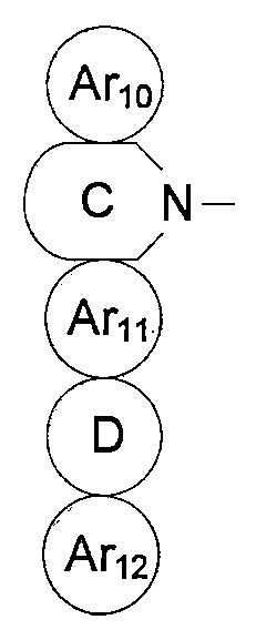
作為予體主體材料,在本發明一實施例中,其分子通式為:
式中,Ar1、Ar2、Ar3和Ar4取代基相同或不同,分別獨立選自亞芳基或亞雜芳基(雜原子特指氮原子);R1、R2、R3和R4的結構為,其中,Ar5、A、Ar6、B和Ar7是以稠環方式連接的,共用2個原子,Ar5、Ar6和Ar7相同或不同,分別獨立選自苯環、取代的苯環、萘環、取代的萘環、蒽環或取代的蒽環,A為含氮原子的五員雜環或六員雜環,B為五員環、五員雜環、六員環或六員雜環(雜原子為氮原子、氧原子、硫原子或硒原子中的一種或兩種)。 In the formula, the substituents of Ar 1 , Ar 2 , Ar 3 and Ar 4 are the same or different, and are independently selected from arylene or heteroarylene (heteroatom especially nitrogen atom); R 1 , R 2 , R 3 and The structure of R 4 is Among them, Ar 5 , A, Ar 6 , B and Ar 7 are connected in a condensed ring manner and share two atoms. Ar 5 , Ar 6 and Ar 7 are the same or different and are independently selected from benzene rings and substituted benzenes. Ring, naphthalene ring, substituted naphthalene ring, anthracene ring or substituted anthracene ring, A is a five-membered heterocyclic ring or a six-membered heterocyclic ring containing nitrogen atom, and B is a five-membered ring, a five-membered heterocyclic ring, a six-membered ring or a six-membered ring Member heterocycle (heteroatom is one or two of nitrogen atom, oxygen atom, sulfur atom or selenium atom).
作為受體主體材料,在本發明一實施例中,其分子通式為:
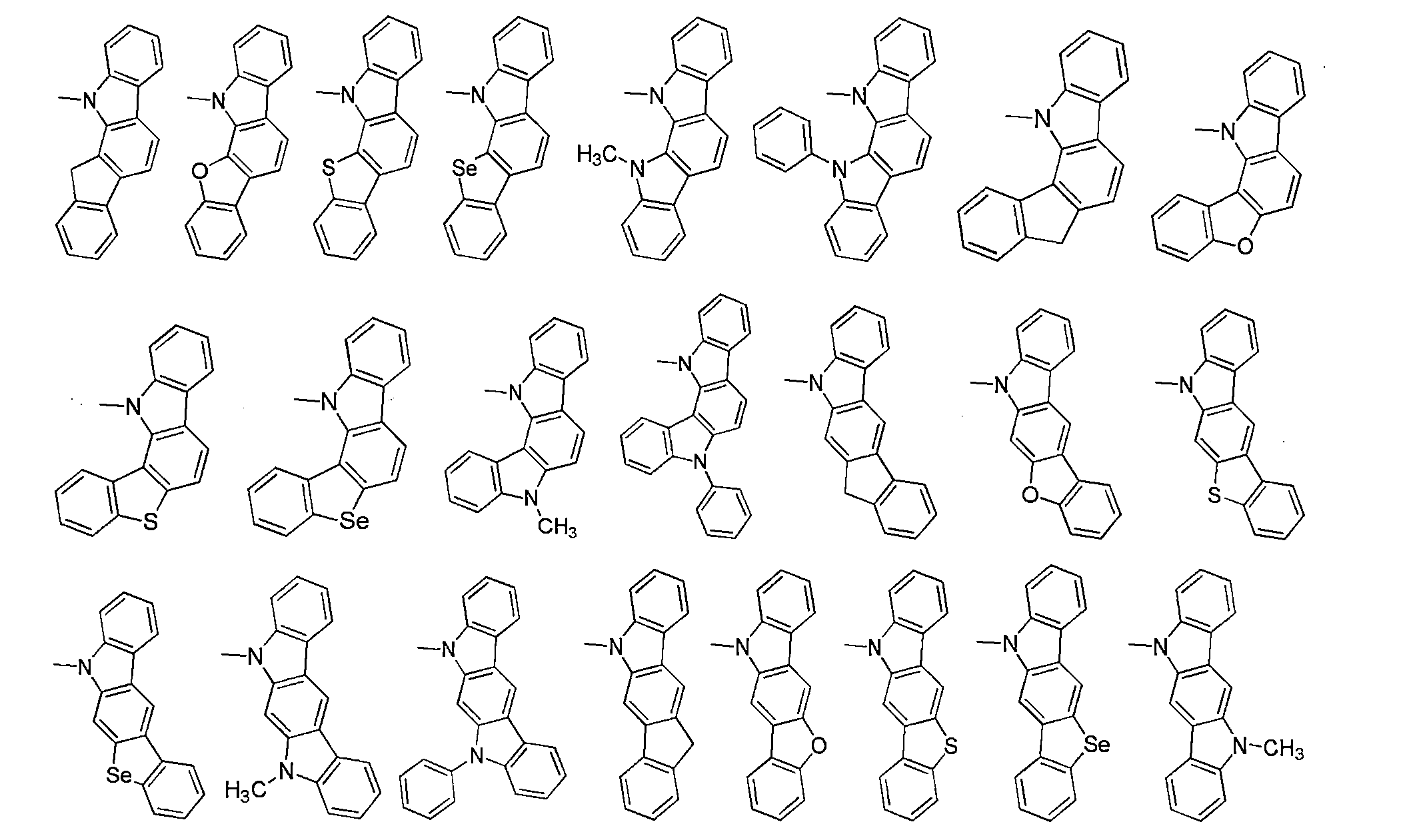
優選地,R1、R2、R3、R4、R5和R6雜環分別獨立選自以下任意分子結構中的一種:
進一步優選地,予體主體材料為具有如下結構的化合物:
優選地,受體主體材料為具有如下結構的化合物:
在將容易給予電子的化合物及容易接受電子的化合物分別用作予體主體材料和受體主體材料時,可以通過設定二者的混合比率來達到最佳的載流子平衡,在該平衡條件下使發光層60內的電洞和電子的複合概率提高且發光效率提高。在本發明一實施例中,予體主體和受體主體的摻雜品質比為1:9~9:1。 When a compound that is easy to donate electrons and a compound that easily accepts electrons are used as the donor host material and the acceptor host material, respectively, the optimal carrier balance can be achieved by setting the mixing ratio of the two. Under this equilibrium condition, The recombination probability of holes and electrons in the light emitting layer 60 is increased, and the light emission efficiency is improved. In an embodiment of the present invention, the doping quality ratio of the donor body and the acceptor body is 1: 9 to 9: 1.
作為磷光材料,在本發明一實施例中,其優選為有機金屬配合物,尤其優選為銥配合物,例如三(2-對甲苯基吡啶)合銥(Ⅲ)(縮寫:Ir(mppy)3)或乙醯丙酮酸二(2-苯基吡啶)合銥(Ⅲ)(縮寫:[Ir(ppy)2(acac)])等。 As a phosphorescent material, in one embodiment of the present invention, it is preferably an organometallic complex, and particularly preferably an iridium complex, such as tris (2-p-tolylpyridine) iridium (III) (abbreviation: Ir (mppy) 3 ) Or acetamidine pyruvate di (2-phenylpyridine) iridium (III) (abbreviation: [Ir (ppy) 2 (acac)]) and the like.
在本發明一實施例中,如圖3所示,電洞傳輸層50和發光層 60之間設置有光學補償層90。在一實施例中,光學補償層90的材料為具有高電洞遷移率的電子阻擋材料,且該電子阻擋材料的三重態能階大於預混的予體主體材料和受體主體材料所形成的激發錯合體的三重態能階。在本發明一實施例中,該光學補償層90的材料為其三重態能階T1>2.6eV的常規電子阻擋材料即可,本發明對其材料不做具體限定。 In an embodiment of the present invention, as shown in FIG. 3, an optical compensation layer 90 is provided between the hole transport layer 50 and the light emitting layer 60. In one embodiment, the material of the optical compensation layer 90 is an electron blocking material with high hole mobility, and the triplet energy level of the electron blocking material is greater than that formed by the premixed pre-host material and the acceptor host material. Excited triplet energy levels of complexes. In an embodiment of the present invention, the material of the optical compensation layer 90 may be a conventional electron blocking material having a triplet energy level T1> 2.6 eV, and the material of the optical compensation layer 90 is not specifically limited in the present invention.
本發明實施例提供的有機電致發光器件,採用高三重態能階的電子阻擋材料作為光學補償層90,不僅在不影響發光器件驅動電壓的情況下,提高了有機電致發光器件,尤其是頂發光有機電致綠光器件的色純度和效率,而且將電子局限在發光層60區域,有利於提高激子的複合機率,進一步提高了器件的發光效率。另外,該實施例中的光學補償層90設置于發光層60和電洞傳輸層50之間,使得光學補償層90和發光層60在蒸鍍過程中,可採用同一組掩膜板製備,能夠避免傳統工藝中由於將光學補償層90設置於電洞注入層40和電洞傳輸層50之間所導致的掩膜板Mask重複對位的問題,在一定程度上提高了工藝精度和良品率。這是由於掩膜板的每次對位元都會有一定誤差,因此對位次數越少,誤差就越少,產品良率也就相應地提高。 The organic electroluminescent device provided by the embodiment of the present invention uses an electron blocking material with a high triplet energy level as the optical compensation layer 90, which not only improves the organic electroluminescent device without affecting the driving voltage of the light emitting device, especially The color purity and efficiency of top-emitting organic electroluminescent green light devices, and limiting the electrons to the area of the light emitting layer 60 are conducive to improving the recombination probability of excitons and further improving the light emitting efficiency of the device. In addition, the optical compensation layer 90 in this embodiment is disposed between the light emitting layer 60 and the hole transmission layer 50, so that during the evaporation process, the optical compensation layer 90 and the light emitting layer 60 can be prepared using the same set of mask plates, which can Avoiding the problem of repetitive alignment of the mask Mask caused by the optical compensation layer 90 disposed between the hole injection layer 40 and the hole transmission layer 50 in the traditional process, which improves the process accuracy and the yield rate to a certain extent. This is because there is a certain error in each alignment of the mask plate, so the fewer the number of alignments, the fewer the errors, and the product yield will increase accordingly.
在本發明另一實施例中,如圖3所示,發光層60和電子傳輸層70間設置有電洞阻擋層(HBL)100,其可通過真空沉積法、濕法或鐳射轉印法等方法形成。作為HBL材料,可以採用任何一種已知的電洞阻擋材料,例如噁二唑衍生物、三唑衍生物或菲咯啉衍生物等。電洞阻擋層100可以有效地阻擋電洞傳輸,將載流子複合限制在發光層60區域,提高了器件的發光效率。 In another embodiment of the present invention, as shown in FIG. 3, a hole blocking layer (HBL) 100 is provided between the light emitting layer 60 and the electron transporting layer 70. The hole blocking layer (HBL) 100 can be formed by a vacuum deposition method, a wet method, or a laser transfer method. Method formation. As the HBL material, any known hole blocking material can be used, such as an oxadiazole derivative, a triazole derivative, or a phenanthroline derivative. The hole blocking layer 100 can effectively block hole transmission, restrict the carrier recombination in the region of the light emitting layer 60, and improve the light emitting efficiency of the device.
基板10為透明的,可以採用玻璃基片或者由聚酯類、聚醯亞胺類等化合物材料構成的柔性基片。 The substrate 10 is transparent, and a glass substrate or a flexible substrate made of a compound material such as polyester or polyimide can be used.
陽極層20可採用無機材料或有機導電聚合物,無機材料一般為氧化銦錫、氧化鋅、氧化銦鋅等金屬氧化物或金、銅、銀等功函數較高的金屬,其中,優選為氧化銦錫(Indium Tin Oxide,ITO),有機導電聚合物優選為聚噻吩/聚乙烯基苯磺酸鈉(縮寫:PEDOT:PSS)、聚苯胺(polyaniline,PANI)中的一種材料。 The anode layer 20 may be an inorganic material or an organic conductive polymer. The inorganic material is generally a metal oxide such as indium tin oxide, zinc oxide, or indium zinc oxide, or a metal with a higher work function such as gold, copper, or silver. Among them, oxidation is preferred. Indium tin (ITO), the organic conductive polymer is preferably one of polythiophene / polyvinylbenzenesulfonate (abbreviation: PEDOT: PSS) and polyaniline (PANI).
陰極層30一般採用鋰、鎂、鈣、鍶、鋁或銦等功函數較低的金屬或它們中的一種與銅、金或銀的合金,或上述金屬分別與合金或金屬氟化物形成的電極層,例如LiF/Al或Mg:Ag合金層/Ag層。 The cathode layer 30 generally uses a metal with a lower work function such as lithium, magnesium, calcium, strontium, aluminum, or indium, or an alloy of one of these with copper, gold, or silver, or an electrode formed by the above metal and an alloy or metal fluoride, respectively. Layer, such as LiF / Al or Mg: Ag alloy layer / Ag layer.
電洞注入層40為包含具有高電洞注入性物質的層,具體可選擇如氧化鉬、氧化鈦、氧化釩、氧化錸、氧化釕、氧化鉻、氧化鋯、氧化銀、氧化鎢和氧化錳等金屬氧化物。此外,還可選擇如酞菁(phthalocyanine,H2Pc)或酞菁銅(II)(copper(II)phyhalocyanine,CuPc)等酞菁類化合物。 The hole injection layer 40 is a layer containing a substance having a high hole injection property. Specifically, for example, molybdenum oxide, titanium oxide, vanadium oxide, hafnium oxide, ruthenium oxide, chromium oxide, zirconia, silver oxide, tungsten oxide, and manganese oxide can be selected. And other metal oxides. In addition, phthalocyanine compounds such as phthalocyanine (H 2 Pc) or copper (II) phyhalocyanine (CuPc) can be selected.
電洞傳輸層50為包含具有高電洞傳輸性物質的層,具體可選擇如NPB、TPD、BPAFLP、4,4’-雙[N-(9,9-二甲基芴-2-基)-N-苯基氨基]聯苯(縮寫:DFLDPBi)和4,4’-雙[N-(螺環-9,9’-聯芴-2-基)-N-苯基氨基]聯苯(縮寫:BSPB)等芳族胺化合物,還可選擇如CBP、CzPA、PCzPA等哢唑衍生物或如t-BuDNA、DNA、DPAnth等蒽衍生物。 The hole transporting layer 50 is a layer containing a substance having a high hole transporting property. Specifically, NPB, TPD, BPAFLP, 4,4'-bis [N- (9,9-dimethylfluoren-2-yl) can be selected. -N-phenylamino] biphenyl (abbreviation: DFLDPBi) and 4,4'-bis [N- (spiro-9,9'-bifluoren-2-yl) -N-phenylamino] biphenyl ( Abbreviation: BSPB) and other aromatic amine compounds. Also selectable are oxazole derivatives such as CBP, CzPA, PCzPA or anthracene derivatives such as t-BuDNA, DNA, DPAnth.
電子傳輸層70為包含具有高電子傳輸性物質的層,具體可選擇如Alq3、三(4-甲基-8-羥基喹啉)鋁(縮寫:Almq3)、雙(10-羥基苯並[h]喹啉)鈹(縮寫:BeBq2)、BAlq、Zn(BOX)2、雙[2-(2-羥基苯基)苯並噻唑]鋅(縮 寫:Zn(BTZ)2)等金屬配合物,也可選擇如2-(4-聯苯基)-5-(4-叔丁基苯基)-1,3,4-噁二唑(縮寫:PBD)、1,3-雙[5-(對叔丁基苯基)-1,3,4-噁二唑-2-基]苯(縮寫:OXD-7)、3-(4-叔丁基苯基)-4-苯基-5-(4-聯苯基)-1,2,4-三唑(縮寫:TAZ)、3-(4-叔丁基苯基)-4-(4-乙基苯基)-5-(4-聯苯基)-1,2,4-三唑(縮寫:p-EtTAZ)、紅菲繞啉(縮寫:BPhen)等雜芳族化合物。 The electron-transporting layer 70 is a layer containing a substance having a high electron-transporting property. Specifically, for example, Alq 3 , tris (4-methyl-8-hydroxyquinoline) aluminum (abbreviation: Almq 3 ), or bis (10-hydroxybenzo) may be selected. [h] quinoline) beryllium (abbreviation: BeBq 2 ), BAlq, Zn (BOX) 2 , bis [2- (2-hydroxyphenyl) benzothiazole] zinc (abbreviation: Zn (BTZ) 2 ) and other metal complexes Materials, can also choose such as 2- (4-biphenyl) -5- (4-tert-butylphenyl) -1,3,4-oxadiazole (abbreviation: PBD), 1,3-bis [5 -(P-tert-butylphenyl) -1,3,4-oxadiazol-2-yl] benzene (abbreviation: OXD-7), 3- (4-tert-butylphenyl) -4-phenyl- 5- (4-biphenyl) -1,2,4-triazole (abbreviation: TAZ), 3- (4-tert-butylphenyl) -4- (4-ethylphenyl) -5- ( Heteroaromatic compounds such as 4-biphenyl) -1,2,4-triazole (abbreviation: p-EtTAZ) and phenanthroline (abbreviation: BPhen).
電子注入層80為包含具有高電子注入性物質的層,可選擇鹼金屬、鹼土金屬和其化合物,如鋰、銫、鈣、氟化鋰、氟化銫、氟化鈣、氟化鉺或者氧化鋰等。下面將通過具體實施例進一步說明本發明提供的有機電致發光器件。但是,本發明並不局限於下列實施例。 The electron injection layer 80 is a layer containing a substance having a high electron injection property, and an alkali metal, an alkaline earth metal, and a compound thereof such as lithium, cesium, calcium, lithium fluoride, cesium fluoride, calcium fluoride, rubidium fluoride, or oxidation can be selected. Lithium, etc. The organic electroluminescence device provided by the present invention will be further described below through specific examples. However, the present invention is not limited to the following examples.
實施例1 Example 1
本實施例中的有機電致發光器件發光層60的主體材料由不同品質比的予體主體材料與受體主體材料預混而成,這些器件的結構如圖3所示。發光層60的主體材料為激發錯合體(其中,予體主體材料為1-2,受體主體材料為2-3,予體主體材料1-2和受體主體材料2-3採用單源蒸鍍的方式形成激發錯合體),主體材料中摻雜的磷光材料為Ir(mppy)3,光學補償層90設置於電洞傳輸層50和發光層60之間,其材料為具有高遷移率的電子阻擋材料mCBP。 The host material of the light-emitting layer 60 of the organic electroluminescence device in this embodiment is made of pre-mixed host materials and acceptor host materials with different quality ratios. The structures of these devices are shown in FIG. 3. The host material of the light-emitting layer 60 is an excited complex (wherein the host host material is 1-2, the acceptor host material is 2-3, and the host host material 1-2 and the acceptor host material 2-3 are single-source steamed. The excitation complex is formed by plating.) The doped phosphorescent material in the host material is Ir (mppy) 3. The optical compensation layer 90 is disposed between the hole transport layer 50 and the light emitting layer 60. Its material is high mobility Electron blocking material mCBP.
本實施例的器件結構如下: The device structure of this embodiment is as follows:
ITO(20nm)/電洞注入層(HATCN,10nm)/電洞傳輸層(TCTA,80nm)/光學補償層(mCBP,70nm)/(予體主體材料(1-2,10nm):受體主體材料(2-3):10%磷光材料Ir(mppy)3/電子傳輸層(TPBi,30nm)/電子注入層(Bphen,10nm)/Mg:Ag(1:4,1nm)/Ag(15nm) ITO (20nm) / hole injection layer (HATCN, 10nm) / hole transport layer (TCTA, 80nm) / optical compensation layer (mCBP, 70nm) / (precursor host material (1-2, 10nm): acceptor host Material (2-3): 10% phosphorescent material Ir (mppy) 3 / electron transport layer (TPBi, 30nm) / electron injection layer (Bphen, 10nm) / Mg: Ag (1: 4, 1nm) / Ag (15nm)
對照例1 Comparative Example 1
該器件結構如下: The device structure is as follows:
ITO(20nm)電洞注入層(HATCN,10nm)/光學補償層(mCBP,150nm)/mCBP(20nm):10%磷光材料Ir(mppy)3/電子傳輸層(TPBi,30nm)/電子注入層(Bphen,10nm)/Mg:Ag(1:4,1nm)/Ag(15nm) ITO (20nm) hole injection layer (HATCN, 10nm) / optical compensation layer (mCBP, 150nm) / mCBP (20nm): 10% phosphorescent material Ir (mppy) 3 / electron transport layer (TPBi, 30nm) / electron injection layer (Bphen, 10nm) / Mg: Ag (1: 4,1nm) / Ag (15nm)
將上面實施例1和對照例1的有機電致發光器件的性能表示在下表1中:
由表1的資料可看出,主體材料由予體主體和受體材料預混後,其電流效率和T97壽命均比未預混(對照例1)高,其中,當予體主體材料(1-2)與受體主體材料(2-3)的品質比為2:3時器件性能最好,與對照例1對比電流效率提升了22%,T97壽命提升了1倍以上,實施例1中的器件壽命T97可以達到1000小時以上。 From the data in Table 1, it can be seen that after the host material is pre-mixed with the pre-host body and the acceptor material, its current efficiency and T97 life are higher than those without pre-mixing (Comparative Example 1). Among them, when the pre-host body material (1 -2) The performance of the device is the best when the quality ratio of the receptor host material (2-3) is 2: 3. Compared with Comparative Example 1, the current efficiency is increased by 22%, and the T97 life is increased by more than double. In Example 1, The device life T97 can reach more than 1000 hours.
實施例2 Example 2
參考實施例1製備有機電致發光器件,其中,予體主體材料為本發明上述予體主體材料1-24,受體主體材料為本發明上述受體主體材料2-10,且二者的品質比為2:3。該器件的性能如表2所示。 Reference Example 1 was used to prepare an organic electroluminescence device. The donor host material was the above-mentioned donor host material 1-24, and the acceptor host material was the above-mentioned acceptor host material 2-10. The ratio is 2: 3. The performance of this device is shown in Table 2.
實施例3 Example 3
參考實施例1製備有機電致發光器件,其中,予體主體材料為本發明上述予體主體材料1-30,受體主體材料為本發明上述受體主體材料2-16,且二者的品質比為2:3,該器件的性能如表2所示。 Reference Example 1 was used to prepare an organic electroluminescence device. The donor host material was the above-mentioned donor host material 1-30, and the acceptor host material was the above-mentioned acceptor host material 2-16. The ratio is 2: 3, and the performance of this device is shown in Table 2.
本發明實施例還提供一種有機電致發光器件的製備方法,該製備方法包括:在基板10上設置陽極20;在陽極20上設置發光層60,該發光層60的主體材料由予體主體材料和受體主體材料預混形成,且予體主體材料和受體主體材料置於同一蒸發源中,進行共蒸鍍而形成激發錯合體,主體材料中摻雜客體材料;以及在發光層60上設置陰極30。 An embodiment of the present invention also provides a method for preparing an organic electroluminescent device. The manufacturing method includes: providing an anode 20 on a substrate 10; and providing a light-emitting layer 60 on the anode 20. It is formed by premixing with the host host material, and the host host material and the host host material are placed in the same evaporation source, and co-evaporation is performed to form an excited complex, and the host material is doped with a guest material; and on the light-emitting layer 60 A cathode 30 is provided.
本發明實施例有效地解決了高亮度下效率滾降(roll-off)下降嚴重的問題,使得器件的穩定性進一步提高,同時減少了客體材料的摻雜濃度,從而降低了產品成本。 The embodiment of the present invention effectively solves the problem of serious reduction in efficiency roll-off at high brightness, which further improves the stability of the device, and reduces the doping concentration of the guest material, thereby reducing the product cost.
在本發明實施例中,該製備方法還包括:在前述陽極20與前 述發光層60之間依序層疊設置電洞注入層40和電洞傳輸層50;以及在前述電洞傳輸層50與前述發光層60之間設置光學補償層90。具體地,在陽極20上設置電洞注入層40,在電洞注入層40上設置電洞傳輸層50,進一步地,在電洞傳輸層50上設置光學補償層90,該光學補償層90位於發光層60之下。 In the embodiment of the present invention, the preparation method further includes: sequentially stacking a hole injection layer 40 and a hole transmission layer 50 between the anode 20 and the light emitting layer 60; and placing the hole transmission layer 50 and the hole An optical compensation layer 90 is provided between the light emitting layers 60. Specifically, a hole injection layer 40 is provided on the anode 20, a hole transmission layer 50 is provided on the hole injection layer 40, and an optical compensation layer 90 is provided on the hole transmission layer 50. The optical compensation layer 90 is located on Under the light emitting layer 60.
在本發明實施例中,可以通過傳統的蒸鍍或塗佈工藝在基板10上依序層疊設置陽極20、電洞注入層40、電洞傳輸層50、光學補償層90、發光層60和陰極30等。 In the embodiment of the present invention, the anode 20, the hole injection layer 40, the hole transmission layer 50, the optical compensation layer 90, the light emitting layer 60, and the cathode can be sequentially stacked on the substrate 10 through a conventional evaporation or coating process. 30 and so on.
以上所述僅為本發明的較佳實施例而已,並不用以限制本發明,凡在本發明的精神和原則之內,所作的任何修改、等同替換等,均應包含在本發明的保護範圍之內。 The above are only the preferred embodiments of the present invention, and are not intended to limit the present invention. Any modification, equivalent replacement, etc. within the spirit and principle of the present invention shall be included in the protection scope of the present invention. within.
工業實用性 Industrial applicability
本發明的有機電致發光器件及其製備方法,通過將發光層60的主體材料由予體主體材料和受體主體材料置於同一蒸發源中,進行共蒸鍍而形成激發錯合體,不僅利於電子與電洞載流子間的平衡,提升了器件的壽命和效率,而且單源蒸鍍降低了工藝操作難度,提高了量產的良率。 The organic electroluminescence device and the preparation method thereof of the present invention form an excited complex by placing the host material of the light-emitting layer 60 from the host host material and the acceptor host material in the same evaporation source and co-evaporation to form an excited complex. The balance between electrons and hole carriers improves the life and efficiency of the device, and single source evaporation reduces the difficulty of process operation and improves the yield of mass production.
Claims (14)




Applications Claiming Priority (2)
| Application Number | Priority Date | Filing Date | Title |
|---|---|---|---|
| CN201710048295.3A CN108336237B (en) | 2017-01-20 | 2017-01-20 | An organic electroluminescent device |
| ??201710048295.3 | 2017-01-20 |
Publications (2)
| Publication Number | Publication Date |
|---|---|
| TW201827628A TW201827628A (en) | 2018-08-01 |
| TWI667360B true TWI667360B (en) | 2019-08-01 |
Family
ID=62908838
Family Applications (1)
| Application Number | Title | Priority Date | Filing Date |
|---|---|---|---|
| TW107101972A TWI667360B (en) | 2017-01-20 | 2018-01-19 | Organic electroluminescent device and preparation method thereof |
Country Status (7)
| Country | Link |
|---|---|
| US (1) | US11158821B2 (en) |
| EP (1) | EP3573118B1 (en) |
| JP (1) | JP6829768B2 (en) |
| KR (1) | KR102254393B1 (en) |
| CN (1) | CN108336237B (en) |
| TW (1) | TWI667360B (en) |
| WO (1) | WO2018133836A1 (en) |
Families Citing this family (16)
| Publication number | Priority date | Publication date | Assignee | Title |
|---|---|---|---|---|
| CA3298593A1 (en) * | 2016-12-02 | 2026-03-02 | The Research Foundation For The State University Of New York | Fabrication method for fused multi-layer amorphous selenium sensor |
| US11479544B2 (en) | 2017-03-08 | 2022-10-25 | Idemitsu Kosan Co., Ltd. | Compound, material for organic electroluminescence element, organic electroluminescence element, and electronic device |
| KR102637792B1 (en) | 2018-03-22 | 2024-02-19 | 삼성디스플레이 주식회사 | Organic light emitting device and electronic device including the same |
| WO2020075014A1 (en) * | 2018-10-10 | 2020-04-16 | Semiconductor Energy Laboratory Co., Ltd. | Light-emitting device, light-emitting apparatus, electronic device, and lighting device |
| CN109638170B (en) * | 2018-11-07 | 2021-10-19 | 北京绿人科技有限责任公司 | An organic electro-optical element |
| JP7393799B2 (en) * | 2018-11-30 | 2023-12-07 | 株式会社Kyulux | Membrane manufacturing method |
| KR102804493B1 (en) | 2019-04-30 | 2025-05-09 | 삼성디스플레이 주식회사 | Organic light emitting device |
| KR102770368B1 (en) | 2020-03-03 | 2025-02-18 | 주식회사 엘지화학 | Novel compound and organic light emitting device comprising the same |
| CN111943829B (en) * | 2020-07-27 | 2022-04-15 | 清华大学 | Exciplex, application thereof and organic electroluminescent device adopting exciplex |
| KR20220085924A (en) | 2020-12-15 | 2022-06-23 | 삼성디스플레이 주식회사 | Light emitting device and electronic apparatus comprising same |
| CN114639786B (en) * | 2020-12-15 | 2025-08-22 | 云谷(固安)科技有限公司 | Light-emitting device and display panel |
| CN112979623B (en) * | 2021-02-22 | 2022-09-09 | 吉林奥来德光电材料股份有限公司 | A five-membered heterocyclic compound and preparation method thereof, organic electroluminescent device and element |
| CN115224208B (en) * | 2021-04-20 | 2026-01-23 | 中国科学院理化技术研究所 | Phosphorescent organic electroluminescent device sensitized by exciplex |
| CN113969168B (en) * | 2021-10-27 | 2024-06-21 | 京东方科技集团股份有限公司 | Red light organic electroluminescent composition, red light organic electroluminescent device and display device containing the same |
| KR20250074833A (en) * | 2023-11-20 | 2025-05-28 | 에스에프씨 주식회사 | Novel Heterocyclic compounds and Organic light emitting diode including the same |
| CN119661546A (en) * | 2025-02-24 | 2025-03-21 | 西安欧得光电材料有限公司 | Organic light-emitting compound and organic electroluminescent device thereof |
Citations (3)
| Publication number | Priority date | Publication date | Assignee | Title |
|---|---|---|---|---|
| CN1303083C (en) * | 2003-02-12 | 2007-03-07 | 昱镭光电科技股份有限公司 | Red organic electroluminescent material |
| CN103515537A (en) * | 2012-06-27 | 2014-01-15 | 三星显示有限公司 | Organic light-emitting device including multi-layered hole transport layer, and organic light-emitting display apparatus including the same |
| KR20150105906A (en) * | 2014-03-10 | 2015-09-18 | 삼성에스디아이 주식회사 | Condensed compound and organic light emitting device including the same |
Family Cites Families (17)
| Publication number | Priority date | Publication date | Assignee | Title |
|---|---|---|---|---|
| KR20050066970A (en) * | 2003-12-26 | 2005-06-30 | 닛토덴코 가부시키가이샤 | Electroluminescence device, planar light source and display using the same |
| EP2564438B1 (en) * | 2010-04-28 | 2016-10-19 | Universal Display Corporation | Depositing premixed materials |
| JP5694019B2 (en) * | 2011-03-17 | 2015-04-01 | 株式会社東芝 | Organic electroluminescent element, display device and lighting device |
| WO2012127990A1 (en) | 2011-03-23 | 2012-09-27 | Semiconductor Energy Laboratory Co., Ltd. | Light-emitting element |
| JP2014187130A (en) * | 2013-03-22 | 2014-10-02 | Nippon Hoso Kyokai <Nhk> | Organic electroluminescent element, display device and illuminating device, evaluation method of hole transport material |
| US10014487B2 (en) * | 2013-09-17 | 2018-07-03 | Kyulux, Inc. | Organic electroluminescent device |
| CN104600213A (en) * | 2013-10-30 | 2015-05-06 | 海洋王照明科技股份有限公司 | Preparation method of organic electroluminescent device |
| KR102315298B1 (en) * | 2014-04-22 | 2021-10-20 | 유니버셜 디스플레이 코포레이션 | Material for phosphorescent light-emitting element |
| CN103985822B (en) * | 2014-05-30 | 2017-05-10 | 广州华睿光电材料有限公司 | Organic mixture, composite containing organic mixture, organic electronic device and application |
| KR102377360B1 (en) * | 2014-08-08 | 2022-03-21 | 가부시키가이샤 한도오따이 에네루기 켄큐쇼 | Light-emitting element, light-emitting device, lighting device, display device, display panel, and electronic appliance |
| TWI666803B (en) * | 2014-09-17 | 2019-07-21 | 日商日鐵化學材料股份有限公司 | Organic electric field light emitting element and manufacturing method thereof |
| CN104538559B (en) * | 2014-12-31 | 2017-10-10 | 北京维信诺科技有限公司 | A kind of organic electroluminescence display device and method of manufacturing same with rgb pixel area |
| CN105895811B (en) * | 2015-01-26 | 2018-03-20 | 北京维信诺科技有限公司 | A kind of thermal activation sensitized fluorescence organic electroluminescence device |
| TWI749726B (en) * | 2015-03-09 | 2021-12-11 | 日商半導體能源研究所股份有限公司 | Light-emitting element, display device, electronic device, and lighting device |
| JP6731908B2 (en) * | 2015-03-30 | 2020-07-29 | 日鉄ケミカル&マテリアル株式会社 | Organic electroluminescent device |
| CN106328816B (en) * | 2015-06-16 | 2018-11-13 | 昆山国显光电有限公司 | A kind of organic electroluminescence device and preparation method thereof |
| KR102646440B1 (en) * | 2015-07-08 | 2024-03-13 | 가부시키가이샤 한도오따이 에네루기 켄큐쇼 | Light-emitting devices, display devices, electronic devices, and lighting devices |
-
2017
- 2017-01-20 CN CN201710048295.3A patent/CN108336237B/en active Active
-
2018
- 2018-01-19 WO PCT/CN2018/073380 patent/WO2018133836A1/en not_active Ceased
- 2018-01-19 EP EP18741504.7A patent/EP3573118B1/en active Active
- 2018-01-19 KR KR1020197015666A patent/KR102254393B1/en active Active
- 2018-01-19 JP JP2019529234A patent/JP6829768B2/en active Active
- 2018-01-19 TW TW107101972A patent/TWI667360B/en active
-
2019
- 2019-01-11 US US16/317,491 patent/US11158821B2/en active Active
Patent Citations (3)
| Publication number | Priority date | Publication date | Assignee | Title |
|---|---|---|---|---|
| CN1303083C (en) * | 2003-02-12 | 2007-03-07 | 昱镭光电科技股份有限公司 | Red organic electroluminescent material |
| CN103515537A (en) * | 2012-06-27 | 2014-01-15 | 三星显示有限公司 | Organic light-emitting device including multi-layered hole transport layer, and organic light-emitting display apparatus including the same |
| KR20150105906A (en) * | 2014-03-10 | 2015-09-18 | 삼성에스디아이 주식회사 | Condensed compound and organic light emitting device including the same |
Also Published As
| Publication number | Publication date |
|---|---|
| CN108336237B (en) | 2020-01-31 |
| TW201827628A (en) | 2018-08-01 |
| WO2018133836A1 (en) | 2018-07-26 |
| JP2020513691A (en) | 2020-05-14 |
| EP3573118B1 (en) | 2023-03-29 |
| US20190165286A1 (en) | 2019-05-30 |
| KR102254393B1 (en) | 2021-05-24 |
| KR20190069584A (en) | 2019-06-19 |
| US11158821B2 (en) | 2021-10-26 |
| JP6829768B2 (en) | 2021-02-10 |
| CN108336237A (en) | 2018-07-27 |
| EP3573118A4 (en) | 2020-01-22 |
| EP3573118A1 (en) | 2019-11-27 |
Similar Documents
| Publication | Publication Date | Title |
|---|---|---|
| TWI667360B (en) | Organic electroluminescent device and preparation method thereof | |
| JP7456997B2 (en) | Molten mixture for organic electroluminescent device and organic electroluminescent device | |
| US11189802B2 (en) | Organic electroluminescent element | |
| CN107078221B (en) | Organic electroluminescence element and manufacturing method thereof | |
| TWI892393B (en) | Light-emitting element | |
| TW201831652A (en) | Material for organic electroluminescent element, and organic electroluminescent element | |
| CN111051313A (en) | Organic compound, light-emitting element, light-emitting device, electronic device, and lighting device | |
| KR102760228B1 (en) | Organic electroluminescent device | |
| TW201840819A (en) | Material for organic electroluminescence element, and organic electroluminescence element | |
| CN113506855A (en) | Organic electroluminescent device, preparation method thereof and display device | |
| JP2025157550A (en) | Organic electroluminescent device | |
| CN115336027A (en) | Organic electroluminescent element | |
| JP2020123477A (en) | Light-emitting element, display device and illumination apparatus | |
| KR102823219B1 (en) | Organic electroluminescent device | |
| CN114916245A (en) | OLED device and manufacturing method | |
| CN116635395A (en) | Organic electroluminescence element | |
| TW202138544A (en) | Organic electroluminescent device | |
| CN113661226A (en) | Organic electroluminescent element | |
| WO2024048536A1 (en) | Organic electroluminescent element | |
| JP2026046735A (en) | Boron-containing compounds, light-emitting materials, organic electroluminescent elements, and electronic devices | |
| WO2024208890A1 (en) | Organic electroluminescent device comprising a organic matrix compound and organic electron transport compound of formula (i), and display device comprising the organic electroluminescent device | |
| Banik | Functional Pyrene–Pyridine-Integrated Hole-Transporting Materials for Solution-Processed OLEDs with Reduced Efficiency Roll-Off |