TWI802199B - semiconductor memory device - Google Patents
semiconductor memory device Download PDFInfo
- Publication number
- TWI802199B TWI802199B TW111100118A TW111100118A TWI802199B TW I802199 B TWI802199 B TW I802199B TW 111100118 A TW111100118 A TW 111100118A TW 111100118 A TW111100118 A TW 111100118A TW I802199 B TWI802199 B TW I802199B
- Authority
- TW
- Taiwan
- Prior art keywords
- data
- transistor
- transistors
- input
- circuit
- Prior art date
Links
Images






Classifications
-
- G—PHYSICS
- G11—INFORMATION STORAGE
- G11C—STATIC STORES
- G11C7/00—Arrangements for writing information into, or reading information out from, a digital store
- G11C7/06—Sense amplifiers; Associated circuits, e.g. timing or triggering circuits
- G11C7/065—Differential amplifiers of latching type
-
- G—PHYSICS
- G11—INFORMATION STORAGE
- G11C—STATIC STORES
- G11C7/00—Arrangements for writing information into, or reading information out from, a digital store
- G11C7/10—Input/output [I/O] data interface arrangements, e.g. I/O data control circuits, I/O data buffers
- G11C7/1078—Data input circuits, e.g. write amplifiers, data input buffers, data input registers, data input level conversion circuits
- G11C7/1087—Data input latches
-
- G—PHYSICS
- G11—INFORMATION STORAGE
- G11C—STATIC STORES
- G11C16/00—Erasable programmable read-only memories
- G11C16/02—Erasable programmable read-only memories electrically programmable
- G11C16/06—Auxiliary circuits, e.g. for writing into memory
- G11C16/26—Sensing or reading circuits; Data output circuits
-
- G—PHYSICS
- G11—INFORMATION STORAGE
- G11C—STATIC STORES
- G11C7/00—Arrangements for writing information into, or reading information out from, a digital store
- G11C7/10—Input/output [I/O] data interface arrangements, e.g. I/O data control circuits, I/O data buffers
- G11C7/1015—Read-write modes for single port memories, i.e. having either a random port or a serial port
- G11C7/1039—Read-write modes for single port memories, i.e. having either a random port or a serial port using pipelining techniques, i.e. using latches between functional memory parts, e.g. row/column decoders, I/O buffers, sense amplifiers
-
- G—PHYSICS
- G11—INFORMATION STORAGE
- G11C—STATIC STORES
- G11C7/00—Arrangements for writing information into, or reading information out from, a digital store
- G11C7/10—Input/output [I/O] data interface arrangements, e.g. I/O data control circuits, I/O data buffers
- G11C7/1051—Data output circuits, e.g. read-out amplifiers, data output buffers, data output registers, data output level conversion circuits
- G11C7/106—Data output latches
-
- G—PHYSICS
- G11—INFORMATION STORAGE
- G11C—STATIC STORES
- G11C7/00—Arrangements for writing information into, or reading information out from, a digital store
- G11C7/10—Input/output [I/O] data interface arrangements, e.g. I/O data control circuits, I/O data buffers
- G11C7/1051—Data output circuits, e.g. read-out amplifiers, data output buffers, data output registers, data output level conversion circuits
- G11C7/1063—Control signal output circuits, e.g. status or busy flags, feedback command signals
-
- G—PHYSICS
- G11—INFORMATION STORAGE
- G11C—STATIC STORES
- G11C7/00—Arrangements for writing information into, or reading information out from, a digital store
- G11C7/10—Input/output [I/O] data interface arrangements, e.g. I/O data control circuits, I/O data buffers
- G11C7/1078—Data input circuits, e.g. write amplifiers, data input buffers, data input registers, data input level conversion circuits
- G11C7/109—Control signal input circuits
-
- G—PHYSICS
- G11—INFORMATION STORAGE
- G11C—STATIC STORES
- G11C16/00—Erasable programmable read-only memories
- G11C16/02—Erasable programmable read-only memories electrically programmable
- G11C16/04—Erasable programmable read-only memories electrically programmable using variable threshold transistors, e.g. FAMOS
- G11C16/0483—Erasable programmable read-only memories electrically programmable using variable threshold transistors, e.g. FAMOS comprising cells having several storage transistors connected in series
-
- G—PHYSICS
- G11—INFORMATION STORAGE
- G11C—STATIC STORES
- G11C2207/00—Indexing scheme relating to arrangements for writing information into, or reading information out from, a digital store
- G11C2207/005—Transfer gates, i.e. gates coupling the sense amplifier output to data lines, I/O lines or global bit lines
-
- G—PHYSICS
- G11—INFORMATION STORAGE
- G11C—STATIC STORES
- G11C7/00—Arrangements for writing information into, or reading information out from, a digital store
- G11C7/06—Sense amplifiers; Associated circuits, e.g. timing or triggering circuits
- G11C7/067—Single-ended amplifiers
Landscapes
- Read Only Memory (AREA)
- Static Random-Access Memory (AREA)
- Semiconductor Memories (AREA)
- Metal-Oxide And Bipolar Metal-Oxide Semiconductor Integrated Circuits (AREA)
- Non-Volatile Memory (AREA)
Abstract
本發明提供一種能提高資料輸入輸出之穩健性之半導體記憶裝置。 實施方式之半導體記憶裝置包含:複數個資料鎖存電路XDL,其等用於在感測放大器電路與輸入輸出電路之間進行資料之輸入輸出;及匯流排XBUS,其連接於複數個資料鎖存電路XDL。資料鎖存電路XDL包含:反相器電路XIV,其暫時保持在感測放大器電路與輸入輸出電路之間輸入輸出之資料;以及N通道型MOS電晶體TN31、TN32及P通道型MOS電晶體TP31,其等並聯設置於反相器電路XIV與匯流排XBUS之間。N通道型MOS電晶體TN31、TN32經多工化。The invention provides a semiconductor memory device capable of improving the robustness of data input and output. The semiconductor memory device of the embodiment includes: a plurality of data latch circuits XDL, which are used to input and output data between the sense amplifier circuit and the input and output circuit; and a bus bar XBUS, which is connected to the plurality of data latch circuits. Circuit XDL. The data latch circuit XDL includes: an inverter circuit XIV, which temporarily holds data input and output between the sense amplifier circuit and the input-output circuit; and N-channel type MOS transistors TN31, TN32 and P-channel type MOS transistor TP31 , which are arranged in parallel between the inverter circuit XIV and the bus bar XBUS. N-channel MOS transistors TN31 and TN32 are multiplexed.
Description
本發明之實施方式係關於一種半導體記憶裝置。Embodiments of the present invention relate to a semiconductor memory device.
先前之半導體記憶裝置具備複數個資料鎖存電路,其等用於感測放大器與輸入輸出電路之間之資料之輸入輸出。複數個資料鎖存電路經由資料配線而相互連接。自感測放大器輸出之資料暫時保持於資料鎖存電路後,經由資料配線自輸入輸出電路輸出。Previous semiconductor memory devices have a plurality of data latch circuits, which are used for input and output of data between the sense amplifier and the input and output circuits. The plurality of data latch circuits are connected to each other via data wiring. The data output from the sense amplifier is temporarily held in the data latch circuit, and then output from the input/output circuit through the data wiring.
根據所揭示之實施方式,提供一種能提高資料輸入輸出之穩健性之半導體記憶裝置。According to the disclosed embodiments, a semiconductor memory device capable of improving the robustness of data input and output is provided.
實施方式之半導體記憶裝置包含:複數個資料鎖存電路,其等用於在感測放大器電路與輸入輸出電路之間進行資料之輸入輸出;及資料配線,其連接於複數個資料鎖存電路。資料鎖存電路包含:資料保持部,其暫時保持在感測放大器電路與輸入輸出電路之間輸入輸出之資料;及N通道型MOS(Metal Oxide Semiconductor,金氧半導體)電晶體及P通道型MOS電晶體中之至少一者,其設置於資料保持部與資料配線之間。N通道型MOS電晶體及P通道型MOS電晶體中之至少一者經多工化。The semiconductor memory device of the embodiment includes: a plurality of data latch circuits for inputting and outputting data between the sense amplifier circuit and the input/output circuit; and data wiring connected to the plurality of data latch circuits. The data latch circuit includes: a data holding unit, which temporarily holds data input and output between the sense amplifier circuit and the input and output circuits; and an N-channel MOS (Metal Oxide Semiconductor, Metal Oxide Semiconductor) transistor and a P-channel MOS At least one of the transistors is disposed between the data holding part and the data wiring. At least one of the N-channel MOS transistor and the P-channel MOS transistor is multiplexed.
以下,參照圖式對實施方式進行說明。為了使說明容易理解,各圖式中對同一構成要素儘量標註相同之符號,從而省略重複之說明。Embodiments will be described below with reference to the drawings. In order to make the description easier to understand, the same components are given the same symbols as much as possible in the drawings, and repeated descriptions are omitted.
<實施方式> (記憶系統之構成) 如圖1所示,本實施方式之記憶系統具備記憶體控制器1及半導體記憶裝置2。半導體記憶裝置2係作為NAND(Not And,反及)型快閃記憶體而構成之非揮發性記憶裝置。記憶系統可與主機連接。主機例如為個人電腦或移動終端等電子設備。再者,雖然圖1中僅圖示出一個半導體記憶裝置2,但實際上記憶系統中設置有複數個半導體記憶裝置2。<Embodiment> (Configuration of memory system) As shown in FIG. 1 , the memory system of this embodiment includes a
記憶體控制器1按照來自主機之寫入請求,對向半導體記憶裝置2寫入資料之動作進行控制。又,記憶體控制器1按照來自主機之讀出請求,對自半導體記憶裝置2讀出資料之動作進行控制。The
於記憶體控制器1與半導體記憶裝置2之間,收發晶片賦能信號/CE、就緒-忙碌信號/RB、指令鎖存賦能信號CLE、位址鎖存賦能信號ALE、寫賦能信號/WE、讀賦能信號RE、/RE、寫保護信號/WP、資料之信號DQ<7:0>、及資料選通信號DQS、/DQS各種信號。Between the
晶片賦能信號/CE係用以啟用半導體記憶裝置2之信號。就緒-忙碌信號/RB係用以表示半導體記憶裝置2為就緒狀態抑或為忙碌狀態之信號。所謂「就緒狀態」,係指可受理來自外部之命令之狀態。所謂「忙碌狀態」,係指不可受理來自外部之命令之狀態。指令鎖存賦能信號CLE係表示信號DQ<7:0>為指令之信號。位址鎖存賦能信號ALE係表示信號DQ<7:0>為位址之信號。寫賦能信號/WE係用以將所接收到之信號取入至半導體記憶裝置2中之信號,每當接收到指令、位址及資料時,由記憶體控制器1使之生效。記憶體控制器1指示半導體記憶裝置2於信號/WE為「L(Low,低)」位準之期間取入信號DQ<7:0>。The chip enable signal /CE is a signal for enabling the
讀賦能信號RE、/RE係用以使記憶體控制器1自半導體記憶裝置2讀出資料之信號。讀賦能信號RE、/RE用以控制例如輸出信號DQ<7:0>時之半導體記憶裝置2之動作時序。寫保護信號/WP係用以指示半導體記憶裝置2禁止資料寫入及抹除之信號。信號DQ<7:0>係於半導體記憶裝置2與記憶體控制器1之間收發之資料之實體,包括指令、位址及資料。資料選通信號DQS、/DQS係用以控制信號DQ<7:0>之輸入輸出時序之信號。The read enable signals RE and /RE are signals used to enable the
記憶體控制器1具備RAM(Random Access Memory,隨機存取記憶體)11、處理器12、主機介面13、ECC(Error Check and Correction,錯誤檢測與校正)電路14及記憶體介面15。其等藉由內部匯流排16而相互連接。The
主機介面13將自主機接收到之請求及用戶資料(寫入資料)等輸出至內部匯流排16。又,主機介面13將自半導體記憶裝置2讀出之用戶資料、及來自處理器12之應答等發送至主機。The
記憶體介面15基於處理器12之指示,對向半導體記憶裝置2寫入用戶資料等之處理、及自半導體記憶裝置2讀出用戶資料等之處理進行控制。The
處理器12統籌控制記憶體控制器1。處理器12為CPU(Central Processing Unit,中央處理單元)或MPU(Micro Processing Unit,微處理單元)等。處理器12於自主機經由主機介面13接收到請求之情形時,按照該請求進行控制。例如,處理器12按照來自主機之請求,指示記憶體介面15向半導體記憶裝置2寫入用戶資料及奇偶校驗碼。又,處理器12按照來自主機之請求,指示記憶體介面15自半導體記憶裝置2讀出用戶資料及奇偶校驗碼。The
處理器12決定RAM11中儲存之用戶資料於半導體記憶裝置2上之儲存區域(記憶區域)。用戶資料經由內部匯流排16儲存於RAM11。處理器12對作為寫入單位之頁單位之資料(頁資料)實施記憶區域之決定。半導體記憶裝置2之1頁中儲存之用戶資料下文亦稱「單元資料」。單元資料一般會被編碼,而以碼字形式儲存於半導體記憶裝置2。本實施方式中,並非一定要編碼。記憶體控制器1亦可將單元資料不經編碼地儲存於半導體記憶裝置2,但圖1中示出了進行編碼之構成作為一例。於記憶體控制器1不進行編碼之情形時,頁資料與單元資料一致。又,可基於1個單元資料生成1個碼字,亦可基於由單元資料分割而成之分割資料生成1個碼字。又,亦可使用複數個單元資料生成1個碼字。The
處理器12逐個單元資料地決定作為寫入目的地之半導體記憶裝置2之記憶區域。半導體記憶裝置2之記憶區域被分配有物理位址。處理器12使用物理位址,管理作為單元資料之寫入目的地之記憶區域。處理器12指定所決定之記憶區域(物理位址),而指示記憶體介面15將用戶資料寫入至半導體記憶裝置2。處理器12管理用戶資料之邏輯位址(由主機管理之邏輯位址)與物理位址之對應。處理器12於接收到來自主機之包含邏輯位址之讀出請求之情形時,特定出與邏輯位址對應之物理位址,並且指定物理位址而指示記憶體介面15讀出用戶資料。The
ECC電路14將RAM11中儲存之用戶資料編碼,生成碼字。又,ECC電路14將自半導體記憶裝置2讀出之碼字解碼。The
RAM11於將自主機接收到之用戶資料向半導體記憶裝置2中記憶以前,暫時儲存該用戶資料,或於將自半導體記憶裝置2讀出之資料向主機發送以前,暫時儲存該資料。RAM11例如為SRAM(Static Random Access Memory,靜態隨機存取記憶體)或DRAM(Dynamic Random Access Memory,動態隨機存取記憶體)等通用記憶體。The
圖1中示出了記憶體控制器1具備ECC電路14及記憶體介面15之構成例。但其實亦可為ECC電路14內置於記憶體介面15中。又,還可為ECC電路14內置於半導體記憶裝置2中。圖1所示之各要素之具體構成及配置並不特別限定。FIG. 1 shows a configuration example in which a
於自主機接收到寫入請求之情形時,圖1之記憶系統按照如下所述而動作。處理器12使作為寫入對象之資料暫時記憶於RAM11。處理器12將RAM11中儲存之資料讀出並輸入至ECC電路14。ECC電路14將所輸入之資料編碼,並將碼字輸入至記憶體介面15。記憶體介面15將所輸入之碼字寫入至半導體記憶裝置2。When a write request is received from the host, the memory system of FIG. 1 operates as follows. The
於自主機接收到讀出請求之情形時,圖1之記憶系統按照如下所述而動作。記憶體介面15將自半導體記憶裝置2讀出之碼字輸入至ECC電路14。ECC電路14將所輸入之碼字解碼,並將解碼所得之資料儲存於RAM11。處理器12將RAM11中儲存之資料經由主機介面13發送至主機。When a read request is received from the host, the memory system in FIG. 1 operates as follows. The
(半導體記憶裝置之概略構成) 如圖2所示,半導體記憶裝置2具備記憶單元陣列21、輸入輸出電路22、邏輯控制電路23、暫存器24、定序器25、電壓產生電路26、列解碼器27、感測放大器28、輸入輸出用焊墊群30、邏輯控制用焊墊群31及電源輸入用端子群32。(Schematic structure of a semiconductor memory device) As shown in FIG.
記憶單元陣列21係記憶資料之部分。記憶單元陣列21具有與複數個位元線及複數個字元線相關聯之複數個記憶單元電晶體而構成。The
輸入輸出電路22與記憶體控制器1之間收發信號DQ<7:0>及資料選通信號DQS、/DQS。又,輸入輸出電路22將信號DQ<7:0>內之指令及位址傳送至暫存器24。進而,輸入輸出電路22與感測放大器28之間收發寫入資料及讀出資料。The input/
邏輯控制電路23自記憶體控制器1接收晶片賦能信號/CE、指令鎖存賦能信號CLE、位址鎖存賦能信號ALE、寫賦能信號/WE、讀賦能信號RE、/RE及寫保護信號/WP。又,邏輯控制電路23將就緒-忙碌信號/RB傳送至記憶體控制器1,向外部通知半導體記憶裝置2之狀態。
暫存器24暫時保持各種資料。例如,暫存器24保持指示寫入動作、讀出動作及抹除動作等之指令。該指令自記憶體控制器1輸入至輸入輸出電路22後,自輸入輸出電路22傳送至暫存器24而加以保持。又,暫存器24亦保持與上述指令對應之位址。該位址自記憶體控制器1輸入至輸入輸出電路22後,自輸入輸出電路22傳送至暫存器24而加以保持。進而,暫存器24還保持表示半導體記憶裝置2之動作狀態之狀態資訊。狀態資訊根據記憶單元陣列21等之動作狀態,由定序器25隨時更新。狀態資訊根據來自記憶體控制器1之請求,作為狀態信號自輸入輸出電路22輸出至記憶體控制器1。The
定序器25基於自記憶體控制器1輸入至輸入輸出電路22及邏輯控制電路23之控制信號,控制包括記憶單元陣列21在內之各部之動作。The
電壓產生電路26係產生記憶單元陣列21中之資料之寫入動作、讀出動作及抹除動作各自所需之電壓之部分。該電壓中包括例如對記憶單元陣列21之複數個字元線及複數個位元線分別施加之電壓等。電壓產生電路26之動作由定序器25控制。The
列解碼器27係包含用以對記憶單元陣列21之複數個字元線分別施加電壓之開關群之電路。列解碼器27自暫存器24接收塊位址及列位址,基於塊位址而選擇塊,並且基於列位址而選擇字元線。列解碼器27切換開關群之開關狀態,以對所選擇之字元線施加來自電壓產生電路26之電壓。列解碼器27之動作由定序器25控制。The
感測放大器28係用以調整對記憶單元陣列21之位元線施加之電壓、或將位元線之電壓讀出並轉換成資料之電路。感測放大器28於資料之讀出時,獲取自記憶單元陣列21之記憶單元電晶體讀出至位元線之資料,並且將所取得之讀出資料傳送至輸入輸出電路22。感測放大器28於資料之寫入時,將經由位元線而寫入之資料傳送至記憶單元電晶體。感測放大器28之動作由定序器25控制。The
輸入輸出用焊墊群30係設置有用以於記憶體控制器1與輸入輸出電路22之間收發各信號之複數個端子(焊墊)之部分。各個端子分別對應於信號DQ<7:0>及資料選通信號DQS、/DQS而個別地設置。The input/
邏輯控制用焊墊群31係設置有用以於記憶體控制器1與邏輯控制電路23之間收發各信號之複數個端子之部分。各個端子分別對應於晶片賦能信號/CE、指令鎖存賦能信號CLE、位址鎖存賦能信號ALE、寫賦能信號/WE、讀賦能信號RE、/RE、寫保護信號/WP及就緒-忙碌信號/RB而個別地設置。The logic
電源輸入用端子群32係設置有用以承接半導體記憶裝置2之動作所需之各電壓之施加的複數個端子之部分。對各個端子施加之電壓中包括電源電壓Vcc、VccQ、Vpp及接地電壓Vss。電源電壓Vcc係作為動作電源而自外部提供之電路電源電壓,例如為3.3 V左右之電壓。電源電壓VccQ例如為1.2 V之電壓。電源電壓VccQ係於記憶體控制器1與半導體記憶裝置2之間收發信號時使用之電壓。電源電壓Vpp係高於電源電壓Vcc之電源電壓,例如為12 V之電壓。The
(記憶單元陣列之電路構成) 其次,對記憶單元陣列21之電路構成進行說明。(Circuit Configuration of Memory Cell Array) Next, the circuit configuration of the
如圖3所示,記憶單元陣列21包含複數個塊BLK。圖3中僅示出了複數個塊BLK中之一個。記憶單元陣列21所具有之其他塊BLK之構成與圖3所示之構成相同。As shown in FIG. 3, the
如圖3所示,塊BLK例如包含4個串單元SU(SU0~SU3)。又,各串單元SU包含複數個NAND串NS。NAND串NS各自包含例如8個記憶單元電晶體MT(MT0~MT7)、及選擇電晶體ST1、ST2。As shown in FIG. 3 , the block BLK includes, for example, four string units SU ( SU0 to SU3 ). Also, each string unit SU includes a plurality of NAND strings NS. Each of the NAND strings NS includes, for example, eight memory cell transistors MT ( MT0 -MT7 ) and selection transistors ST1 and ST2 .
再者,記憶單元電晶體MT之個數並不限於8個,例如亦可為32個、48個、64個、96個。例如,為了提高截止特性,選擇電晶體ST1、ST2亦可各自由複數個電晶體構成,而非由單個電晶體構成。進而,記憶單元電晶體MT與選擇電晶體ST1、ST2之間亦可設置有虛設單元電晶體。Furthermore, the number of memory unit transistors MT is not limited to 8, for example, it can also be 32, 48, 64, or 96. For example, in order to improve the cut-off characteristic, the selection transistors ST1 and ST2 can also be composed of a plurality of transistors instead of a single transistor. Furthermore, a dummy unit transistor may also be provided between the memory unit transistor MT and the selection transistors ST1 and ST2.
記憶單元電晶體MT以串聯連接於選擇電晶體ST1與選擇電晶體ST2之間之方式配置。一端側之記憶單元電晶體MT7連接於選擇電晶體ST1之源極,另一端側之記憶單元電晶體MT0連接於選擇電晶體ST2之汲極。The memory cell transistor MT is arranged to be connected in series between the selection transistor ST1 and the selection transistor ST2. The memory unit transistor MT7 at one end is connected to the source of the selection transistor ST1, and the memory unit transistor MT0 at the other end is connected to the drain of the selection transistor ST2.
串單元SU0~SU3各自之選擇電晶體ST1之閘極分別共通連接於選擇閘極線SGD0~SGD3。選擇電晶體ST2之閘極在位於同一塊BLK內之複數個串單元SU間共通連接於同一根選擇閘極線SGS。位於同一塊BLK內之記憶單元電晶體MT0~MT7之閘極分別共通連接於字元線WL0~WL7。即,字元線WL0~WL7及選擇閘極線SGS於同一塊BLK內之複數個串單元SU0~SU3間共通,而選擇閘極線SGD即便於同一塊BLK內亦針對每個串單元SU0~SU3個別地設置。The gates of the respective select transistors ST1 of the string units SU0 - SU3 are commonly connected to the select gate lines SGD0 - SGD3 . The gates of the selection transistor ST2 are commonly connected to the same selection gate line SGS among a plurality of string units SU located in the same block BLK. The gates of the memory cell transistors MT0 - MT7 located in the same BLK are respectively connected to the word lines WL0 - WL7 . That is, the word lines WL0-WL7 and the selection gate line SGS are shared among the plurality of string units SU0-SU3 in the same block BLK, and the selection gate line SGD is for each string unit SU0-SU3 even in the same block BLK. SU3 is set individually.
於記憶單元陣列21,設置有n個位元線BL(BL0、BL1、…、BL(n-1))。「n」係與1個串單元SU中包含之NAND串NS之個數對應之整數。例如,於半導體記憶裝置2以將16 kByte資料作為1個單位而寫入至記憶單元陣列21或自記憶單元陣列21讀出之方式構成之情形時,「n」為131072(2之17次冪)。NAND串NS各自之選擇電晶體ST1之汲極連接於對應之位元線BL。NAND串NS各自之選擇電晶體ST2之源極連接於源極線SL。源極線SL相對於塊BLK所具有之複數個選擇電晶體ST2之源極共通。In the
位於同一塊BLK內之複數個記憶單元電晶體MT中記憶之資料會被一次性抹除。另一方面,資料之讀出及寫入係對連接於1個字元線WL且屬於1個串單元SU之複數個記憶單元電晶體MT統一進行。The data memorized in the plurality of memory unit transistors MT located in the same block of BLK will be erased at one time. On the other hand, reading and writing of data are collectively performed on a plurality of memory cell transistors MT connected to one word line WL and belonging to one string unit SU.
再者,於以下之說明中,將連接於1個字元線WL且屬於1個串單元SU之複數個記憶單元電晶體MT所記憶之1位元資料之集合稱為「頁」。於圖3中,對如上所述之由複數個記憶單元電晶體MT構成之集合之一標註了符號「MG」。Furthermore, in the following description, a collection of 1-bit data stored in a plurality of memory unit transistors MT connected to one word line WL and belonging to one string unit SU is referred to as a "page". In FIG. 3 , a symbol "MG" is attached to one of the above-mentioned sets composed of a plurality of memory cell transistors MT.
(感測放大器之構成) 感測放大器28包含與n個位元線BL分別相關聯之n個感測放大器電路。圖4表示n個感測放大器電路中之1個感測放大器電路SAC之電路構成。(Configuration of Sense Amplifier) The
如圖4所示,感測放大器電路SAC包含感測放大器部SA、及資料鎖存電路SDL、ADL、BDL、CDL、XDL。感測放大器部SA、及資料鎖存電路SDL、ADL、BDL、CDL、XDL以可相互收發資料之方式藉由匯流排LBUS而連接。更詳細而言,資料鎖存電路SDL、ADL、BDL、CDL經由匯流排LBUS而共通連接,資料鎖存電路XDL連接於匯流排DBUS。匯流排LBUS及匯流排DBUS經由電晶體TRXX而連接。電晶體TRXX之閘極被輸入控制信號SW。控制信號SW例如由定序器25生成。As shown in FIG. 4 , the sense amplifier circuit SAC includes a sense amplifier section SA and data latch circuits SDL, ADL, BDL, CDL, and XDL. The sense amplifier section SA and the data latch circuits SDL, ADL, BDL, CDL, and XDL are connected through the bus LBUS so that data can be exchanged with each other. More specifically, the data latch circuits SDL, ADL, BDL, and CDL are commonly connected via the bus bar LBUS, and the data latch circuit XDL is connected to the bus bar DBUS. Bus bar LBUS and bus bar DBUS are connected via transistor TRXX. The gate of the transistor TRXX is input with the control signal SW. The control signal SW is generated by the
感測放大器部SA例如於讀出動作中,感測讀出至對應之位元線BL之資料,並判定所讀出之資料為「0」抑或為「1」。感測放大器部SA例如包含為P通道型MOS電晶體之電晶體TR1、為N通道型MOS電晶體之電晶體TR2~TR9、及電容器C10。For example, in the read operation, the sense amplifier unit SA senses the data read out to the corresponding bit line BL, and determines whether the read data is “0” or “1”. The sense amplifier section SA includes, for example, a transistor TR1 that is a P-channel MOS transistor, transistors TR2 to TR9 that are N-channel MOS transistors, and a capacitor C10 .
電晶體TR1之一端連接於電源線,電晶體TR1之另一端連接於電晶體TR2。電晶體TR1之閘極連接於資料鎖存電路SDL內之節點INV。電晶體TR2之一端連接於電晶體TR1,電晶體TR2之另一端連接於節點COM。對電晶體TR2之閘極輸入控制信號BLX。電晶體TR3之一端連接於節點COM,電晶體TR3之另一端連接於電晶體TR4。對電晶體TR3之閘極輸入控制信號BLC。電晶體TR4為高耐壓之MOS電晶體。電晶體TR4之一端連接於電晶體TR3。電晶體TR4之另一端連接於對應之位元線BL。對電晶體TR4之閘極輸入控制信號BLS。One end of the transistor TR1 is connected to the power line, and the other end of the transistor TR1 is connected to the transistor TR2. The gate of the transistor TR1 is connected to the node INV in the data latch circuit SDL. One end of the transistor TR2 is connected to the transistor TR1, and the other end of the transistor TR2 is connected to the node COM. The control signal BLX is input to the gate of the transistor TR2. One end of the transistor TR3 is connected to the node COM, and the other end of the transistor TR3 is connected to the transistor TR4. The control signal BLC is input to the gate of the transistor TR3. Transistor TR4 is a high withstand voltage MOS transistor. One end of transistor TR4 is connected to transistor TR3. The other end of the transistor TR4 is connected to the corresponding bit line BL. A control signal BLS is input to the gate of transistor TR4.
電晶體TR5之一端連接於節點COM,電晶體TR5之另一端連接於節點SRC。電晶體TR5之閘極連接於節點INV。電晶體TR6之一端連接於電晶體TR1與電晶體TR2之間,電晶體TR6之另一端連接於節點SEN。對電晶體TR6之閘極輸入控制信號HLL。電晶體TR7之一端連接於節點SEN,電晶體TR7之另一端連接於節點COM。對電晶體TR7之閘極輸入控制信號XXL。One end of the transistor TR5 is connected to the node COM, and the other end of the transistor TR5 is connected to the node SRC. The gate of transistor TR5 is connected to node INV. One end of the transistor TR6 is connected between the transistor TR1 and the transistor TR2, and the other end of the transistor TR6 is connected to the node SEN. The control signal HLL is input to the gate of the transistor TR6. One end of the transistor TR7 is connected to the node SEN, and the other end of the transistor TR7 is connected to the node COM. Input control signal XXL to the gate of transistor TR7.
電晶體TR8之一端接地,電晶體TR8之另一端連接於電晶體TR9。電晶體TR8之閘極連接於節點SEN。電晶體TR9之一端連接於電晶體TR8,電晶體TR9之另一端連接於匯流排LBUS。對電晶體TR9之閘極輸入控制信號STB。電容器C10之一端連接於節點SEN。對電容器C10之另一端輸入時脈CLK。One end of the transistor TR8 is grounded, and the other end of the transistor TR8 is connected to the transistor TR9. The gate of transistor TR8 is connected to node SEN. One end of the transistor TR9 is connected to the transistor TR8, and the other end of the transistor TR9 is connected to the bus bar LBUS. The control signal STB is input to the gate of the transistor TR9. One end of the capacitor C10 is connected to the node SEN. The clock pulse CLK is input to the other end of the capacitor C10.
控制信號BLX、BLC、BLS、HLL、XXL、STB例如由定序器25生成。又,對連接於電晶體TR1之一端之電源線,例如施加半導體記憶裝置2之內部電源電壓即電壓Vdd,對節點SRC例如施加半導體記憶裝置2之接地電壓即電壓Vss。The control signals BLX, BLC, BLS, HLL, XXL, and STB are generated by the
資料鎖存電路SDL、ADL、BDL、CDL、XDL暫時保持讀出資料。資料鎖存電路XDL連接於輸入輸出電路22,使用於在感測放大器電路SAC與輸入輸出電路22之間進行資料之輸入輸出。The data latch circuits SDL, ADL, BDL, CDL, and XDL temporarily hold readout data. The data latch circuit XDL is connected to the I/
資料鎖存電路SDL例如包含反相器IV11、IV12、及為N通道型MOS電晶體之電晶體TR13、TR14。反相器IV11之輸入節點連接於節點LAT。反相器IV11之輸出節點連接於節點INV。反相器IV12之輸入節點連接於節點INV。反相器IV12之輸出節點連接於節點LAT。電晶體TR13之一端連接於節點INV,電晶體TR13之另一端連接於匯流排LBUS。對電晶體TR13之閘極輸入控制信號STI。電晶體TR13之一端連接於節點LAT,電晶體TR14之另一端連接於匯流排LBUS。對電晶體TR14之閘極輸入控制信號STL。The data latch circuit SDL includes, for example, inverters IV11, IV12, and transistors TR13, TR14 which are N-channel MOS transistors. The input node of the inverter IV11 is connected to the node LAT. The output node of the inverter IV11 is connected to the node INV. The input node of inverter IV12 is connected to node INV. The output node of inverter IV12 is connected to node LAT. One end of the transistor TR13 is connected to the node INV, and the other end of the transistor TR13 is connected to the bus bar LBUS. The control signal STI is input to the gate of the transistor TR13. One end of the transistor TR13 is connected to the node LAT, and the other end of the transistor TR14 is connected to the bus LBUS. The control signal STL is input to the gate of the transistor TR14.
例如,節點LAT中保持之資料,相當於資料鎖存電路SDL中保持之資料。又,節點INV中保持之資料,相當於節點LAT中保持之資料之反相資料。資料鎖存電路ADL、BDL、CDL之電路構成例如與資料鎖存電路SDL之電路構成相同,因此省略其等之說明。以下,將資料鎖存電路ADL、BDL、CDL統稱為「資料鎖存電路DL」。資料鎖存電路XDL之電路構成將於下文加以敍述。For example, the data held in the node LAT is equivalent to the data held in the data latch circuit SDL. Also, the data held in the node INV corresponds to the inverse data of the data held in the node LAT. The circuit configuration of the data latch circuits ADL, BDL, and CDL is, for example, the same as that of the data latch circuit SDL, and therefore description thereof is omitted. Hereinafter, the data latch circuits ADL, BDL, and CDL are collectively referred to as "data latch circuits DL". The circuit configuration of the data latch circuit XDL will be described below.
如圖5所示,感測放大器28具有k個感測放大器單元SAU(SAU0~SAU(k-1))。1個感測放大器單元SAU包含m個感測放大器部SA(SA0~SA(m-1))、m個資料鎖存電路DL(DL0~DL(m-1))、及m個資料鎖存電路XDL(XDL0~XDL(m-1))。「m」及「k」為整數,滿足「m×k=n」。「m」例如為16(2之4次冪),「k」為8192(2之13次冪)。換言之,n(131072,2之17次冪)個感測放大器電路SAC分割成k(8192,2之13次冪)個感測放大器單元SAU,各感測放大器單元SAU包含m(16,2之4次冪)個感測放大器電路SAC。As shown in FIG. 5 , the
m個資料鎖存電路XDL0~XDL(m-1)經由m根匯流排XBUS(XBUS0~XBUS(m-1))連接於輸入輸出電路22。m根匯流排XBUS0~XBUS(m-1)例如相對於32~64個複數個感測放大器單元SAU而共通設置。換言之,於m根匯流排XBUS0~XBUS(m-1),連接有複數個例如32~64個感測放大器單元SAU。複數個感測放大器單元SAU經由匯流排XBUS0~XBUS(m-1)連接於輸入輸出電路22。將如此連接複數個感測放大器單元SAU之匯流排XBUS0~XBUS(m-1)設為一組,複數組匯流排XBUS0~XBUS(m-1)連接於輸入輸出電路22。本實施方式中,匯流排XBUS相當於資料配線。The m data latch circuits XDL0 to XDL(m−1) are connected to the input/
輸入輸出電路22包含資料轉換部220及輸入輸出控制部221。資料轉換部220及輸入輸出控制部221經由複數根配線XL而相互連接。The I/
資料轉換部220藉由在讀出動作時作為串列器發揮功能,而將自資料鎖存電路XDL0~XDL(m-1)經由匯流排XBUS0~XBUS(m-1)分別傳送之並行資料轉換成串列信號,並經由複數根配線XL將其發送至輸入輸出控制部221。資料轉換部220藉由在寫入動作時作為解串器發揮功能,而將自輸入輸出控制部221經由複數根配線XL發送之串列信號轉換成並行資料,並將其分別傳送至匯流排XBUS0~XBUS(m-1)。The
輸入輸出控制部221係控制複數根輸入輸出線I/O與複數根配線XL之間之串列信號傳送之部分。The input-
(資料鎖存電路XDL之構成) 其次,對資料鎖存電路XDL之構成進行說明。(Configuration of Data Latch Circuit XDL) Next, the configuration of the data latch circuit XDL will be described.
如圖6所示,資料鎖存電路XDL包含為P通道型MOS電晶體之TP11~14、TP21、TP31、及為N通道型MOS電晶體之TN11~13、TN21、TN31、TN32。As shown in FIG. 6 , the data latch circuit XDL includes TP11-14, TP21, TP31 which are P-channel MOS transistors, and TN11-13, TN21, TN31, TN32 which are N-channel MOS transistors.
電晶體TP11、TP12、TN11、TN12構成了交叉連接之反相器電路XIV。即,電晶體TP11、TN11構成了第1反相器電路,於節點LAT串聯連接。電晶體TP11、TN11各自之閘極連接於節點INV。節點LAT及節點INV分別作為第1反相器電路之輸出及輸入發揮功能。電晶體TP12、TN12構成了第2反相器電路,於節點INV串聯連接。電晶體TP12、TN12各自之閘極連接於節點LAT。節點LAT及節點INV分別作為第2反相器電路之輸入及輸出發揮功能。Transistors TP11, TP12, TN11, TN12 constitute a cross-connected inverter circuit XIV. That is, transistors TP11 and TN11 constitute a first inverter circuit, and are connected in series at node LAT. The respective gates of the transistors TP11 and TN11 are connected to the node INV. Node LAT and node INV function as the output and input of the first inverter circuit, respectively. Transistors TP12 and TN12 constitute a second inverter circuit and are connected in series at node INV. The respective gates of the transistors TP12 and TN12 are connected to the node LAT. Node LAT and node INV function as the input and output of the second inverter circuit, respectively.
電晶體TP11之電流路徑之2個端部中,與連接於節點LAT之端部為相反側之端部經由電晶體TP13連接於電源電位節點VDD。電源電位節點VDD被供給電源電位Vdd。電晶體TP13之閘極被輸入由定序器25生成之控制信號XLL。電晶體TP13作為基於控制信號XLL而接通/斷開之開關電路發揮功能。Of the two ends of the current path of transistor TP11 , the end opposite to the end connected to node LAT is connected to power supply potential node VDD via transistor TP13 . The power supply potential node VDD is supplied with a power supply potential Vdd. The gate of the transistor TP13 is input with the control signal XLL generated by the
電晶體TP12之電流路徑之2個端部中,與連接於節點INV之端部為相反側之端部經由電晶體TP14連接於電源電位節點VDD。電晶體TP14之閘極被輸入由定序器25生成之控制信號XLI。電晶體TP12作為基於控制信號XLI而接通/斷開之開關電路發揮功能。Of the two ends of the current path of transistor TP12 , the end opposite to the end connected to node INV is connected to power supply potential node VDD via transistor TP14 . The gate of the transistor TP14 is input with the control signal XLI generated by the
電晶體TN11之電流路徑之2個端部中,與連接於節點LAT之端部為相反側之端部經由電晶體TN13連接於接地電位節點VSS。接地電位節點VSS被供給接地電位Vss。電晶體TN13之閘極被輸入由定序器25生成之控制信號XNL。電晶體TN13作為基於控制信號XNL而接通/斷開之開關電路發揮功能。Of the two ends of the current path of transistor TN11 , the end opposite to the end connected to node LAT is connected to ground potential node VSS via transistor TN13 . The ground potential node VSS is supplied with a ground potential Vss. The gate of the transistor TN13 is input with the control signal XNL generated by the
電晶體TN12之電流路徑之2個端部中,與連接於節點INV之端部為相反側之端部連接於接地電位節點VSS。Of the two ends of the current path of the transistor TN12, the end opposite to the end connected to the node INV is connected to the ground potential node VSS.
電晶體TP21、TN21並聯連接於匯流排DBUS與節點INV之間。電晶體TP21之閘極被輸入由定序器25生成之控制信號XNI。電晶體TN21之閘極被輸入由定序器25生成之控制信號XTI。電晶體TP21、TN21作為基於控制信號XNI、XTI而接通/斷開之開關電路發揮功能。The transistors TP21 and TN21 are connected in parallel between the bus bar DBUS and the node INV. The gate of the transistor TP21 is input with the control signal XNI generated by the
電晶體TP31、TN31、TN32連接於匯流排XBUS與節點LAT之間。電晶體TN31、TN32串聯連接。電晶體TP31與串聯連接之電晶體TN31、TN32並聯連接。電晶體TP31之閘極被輸入由定序器25生成之控制信號XNL。電晶體TN31、TN32各自之閘極被輸入由定序器25生成之控制信號XTL。電晶體TP31、TN31、TN32作為基於控制信號XNL、XTL而接通/斷開之開關電路發揮功能。本實施方式中,電晶體TN31、TN32相當於多工化之電晶體。The transistors TP31, TN31, TN32 are connected between the bus XBUS and the node LAT. Transistors TN31 and TN32 are connected in series. Transistor TP31 is connected in parallel with transistors TN31 and TN32 connected in series. The gate of the transistor TP31 is input with the control signal XNL generated by the
(半導體記憶裝置之剖面構造) 如圖7所示,半導體記憶裝置2具有於半導體基板40上依序配置了周邊電路PER及記憶單元陣列21之構造。(Cross-sectional structure of semiconductor memory device) As shown in FIG.
記憶單元陣列21中,於導電體層520之上形成有複數個NAND串NS。導電體層520亦稱嵌入源極線(BSL),相當於圖3之源極線SL。In the
於導電體層520之上方,積層有作為選擇閘極線SGS發揮功能之配線層533、作為字元線WL發揮功能之複數個配線層532、及作為選擇閘極線SGD發揮功能之配線層531。於積層之各配線層533、532、531之間,配置有未圖示之絕緣層。On the
於記憶單元陣列21,形成有複數個記憶孔534。記憶孔534係於上下方向上貫通配線層533、532、531及位於其等之間之未圖示之絕緣層並抵達導電體層520之孔穴。A plurality of
記憶孔534中與積層之配線層533、532、531分別交叉之各部分作為電晶體發揮功能。上述複數個電晶體中,位於與配線層531交叉之部分之電晶體作為選擇電晶體ST1發揮功能。複數個電晶體中,位於與配線層532交叉之部分之電晶體作為記憶單元電晶體MT(MT0~MT7)發揮功能。複數個電晶體中,位於與配線層533交叉之部分之電晶體作為選擇電晶體ST2發揮功能。Each part of the
於記憶孔534之上方,形成有作為位元線BL發揮功能之配線層616。記憶孔534之上端經由接觸插塞539連接於配線層616。Above the
沿著圖7之紙面之進深方向,排列有複數個與圖7所示之構造相同之構造。由沿著圖7之紙面之進深方向排成一行之複數個NAND串NS之集合,形成了1個串單元SU。A plurality of structures identical to those shown in FIG. 7 are arranged along the depth direction of the paper surface of FIG. 7 . One string unit SU is formed by a collection of a plurality of NAND strings NS arranged in a row along the depth direction of the sheet of FIG. 7 .
半導體基板40與導電體層520(源極線SL)相隔而配置,兩者之間配置有周邊電路PER之一部分。周邊電路PER係為了實現記憶單元陣列21中之資料之寫入動作、讀出動作及抹除動作等而設置之電路。圖2所示之感測放大器28、列解碼器27及電壓產生電路26等成為了周邊電路PER之一部分。The
周邊電路PER包含形成於半導體基板40之上表面之電晶體TR、及複數個導電體611~615。導電體611~615係由例如金屬等導體形成之配線層。導電體611~615以分佈於複數個高度位置之方式形成,經由接點620~623而相互電性連接。接點620~623係藉由以於上下方向上貫穿未圖示之絕緣層之方式形成接觸孔後,向該接觸孔之內側填充例如鎢等導電體材料而形成。導電體615經由接點624電性連接於配線層616(位元線BL)。The peripheral circuit PER includes a transistor TR formed on the upper surface of the
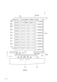
圖8模式性地表示半導體記憶裝置2之周邊電路PER之構造之一部分,尤其是構成資料鎖存電路XDL之部分之平面構造。再者,圖8中示出了構成2個資料鎖存電路XDL1、XDL2之部分之平面構造。FIG. 8 schematically shows part of the structure of the peripheral circuit PER of the
如圖8所示,於半導體記憶裝置2中,依序配置有源極・汲極部LW1、閘極部LT1、源極・汲極部LW2、閘極部LT2、源極・汲極部LW3及閘極部LT3。As shown in FIG. 8, in the
源極・汲極部LW1配置有作為資料鎖存電路XDL1、XDL2各自之電晶體TN31各自之源極或汲極發揮功能之源極・汲極部LW1_1、LW1_2。源極・汲極部LW1_1、LW1_2連接於匯流排XBUS。於閘極部LT1,配置有作為資料鎖存電路XDL1、XDL2各自之電晶體TN31之閘極發揮功能之閘極部LT1_1、LT1_2。於閘極部LT1_1、LT1_2,分別形成有連接於電晶體TN31之閘極之通孔V31。於源極・汲極部LW2,配置有作為資料鎖存電路XDL1、XDL2各自之電晶體TN31之源極或汲極發揮功能,且作為電晶體TN32之源極或汲極發揮功能之源極・汲極部LW2_1、LW2_2。The source-drain part LW1 is provided with the source-drain part LW1_1, LW1_2 which functions as the source or the drain of the transistor TN31 of each data latch circuit XDL1, XDL2, respectively. The source and drain parts LW1_1 and LW1_2 are connected to the bus XBUS. In the gate part LT1, the gate parts LT1_1 and LT1_2 which function as the gate of the transistor TN31 of each data latch circuit XDL1 and XDL2 are arrange|positioned. Via holes V31 connected to the gate of the transistor TN31 are respectively formed in the gate portions LT1_1 and LT1_2 . In the source/drain portion LW2, a source that functions as the source or drain of the transistor TN31 of the data latch circuits XDL1 and XDL2 and that functions as the source or drain of the transistor TN32 is disposed. Drain parts LW2_1, LW2_2.
於閘極部LT2,配置有作為資料鎖存電路XDL1、XDL2各自之電晶體TN32之閘極發揮功能之閘極部LT2_1、LT2_2。於閘極部LT2_1、LT2_2,分別形成有連接於電晶體TN32之閘極之通孔V32。於源極・汲極部LW3,配置有作為資料鎖存電路XDL1、XDL2各自之電晶體TN32之源極或汲極發揮功能,且作為電晶體TN11之源極或汲極發揮功能之源極・汲極部LW3_1、LW3_2。源極・汲極部LW3_1、LW3_2連接於節點LAT。於閘極部LT3,配置有作為資料鎖存電路XDL1、XDL2各自之電晶體TN11之閘極發揮功能之閘極部LT3_1、LT3_2。In the gate part LT2, the gate parts LT2_1 and LT2_2 which function as the gate of the transistor TN32 of each data latch circuit XDL1 and XDL2 are arrange|positioned. Via holes V32 connected to the gate of the transistor TN32 are respectively formed in the gate portions LT2_1 and LT2_2 . In the source/drain portion LW3, a source that functions as the source or drain of the transistor TN32 of the data latch circuits XDL1 and XDL2 and that functions as the source or drain of the transistor TN11 is disposed. Drain part LW3_1, LW3_2. The source/drain parts LW3_1 and LW3_2 are connected to the node LAT. In the gate part LT3, the gate parts LT3_1 and LT3_2 which function as the gate of the transistor TN11 of each data latch circuit XDL1 and XDL2 are arrange|positioned.
將配置各部LW1、LT1、LW2、LT2、LW3、LT3之方向設為進深方向Y時,通孔V31及通孔V32配置於與進深方向Y平行之同一直線上。於通孔V31及通孔V32,連接有沿著進深方向Y延伸之共通之配線LTG。控制信號XTL自定序器25經由配線LTG輸入至通孔V31及通孔V32。本實施方式中,配線LTG相當於共通之信號線。When the direction in which the parts LW1, LT1, LW2, LT2, LW3, and LT3 are arranged is the depth direction Y, the through hole V31 and the through hole V32 are arranged on the same straight line parallel to the depth direction Y. The common wiring LTG extending along the depth direction Y is connected to the through hole V31 and the through hole V32. The control signal XTL is input from the
本實施方式之半導體記憶裝置2如圖8所示,採用了所謂之雙閘極方式,即各資料鎖存電路XDL1、XDL2之電晶體TN31之閘極、及電晶體TN32之閘極設置於不同之部分。於採用雙閘極方式之情形時,如圖8所示,可將構成一資料鎖存電路XDL1之各部LW1_1、LT1_1、LW2_1、LT2_1、LW3_1、LT3_1與構成另一資料鎖存電路XDL2之各部LW1_2、LT1_2、LW2_2、LT2_2、LW3_2、LT3_2沿著橫向X排列而配置。The
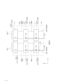
另一方面,於如圖9所示地製造半導體記憶裝置2之情形時,亦可設置雙重化之電晶體TN31、TN32。於圖9所示之參考例之半導體記憶裝置2中,依序配置有源極・汲極部LW1、閘極部LT1、源極・汲極部LW2、閘極部LT2、源極・汲極部LW3、間隙部LG、源極・汲極部LW4及閘極部LT3。On the other hand, when manufacturing the
源極・汲極部LW1作為另一資料鎖存電路XDL2之電晶體TN31、TN32各自之源極或汲極發揮功能。源極・汲極部LW1連接於節點LAT。閘極部LT1作為另一資料鎖存電路XDL2之電晶體TN31、TN32各自之閘極發揮功能。於閘極部LT1,設置有連接於電晶體TN31、TN32各自之閘極之通孔V31、V32。源極・汲極部LW2作為一資料鎖存電路XDL1之電晶體TN31、TN32各自之源極或汲極發揮功能,且作為另一資料鎖存電路XDL2之電晶體TN31、TN32各自之源極或汲極發揮功能。源極・汲極部LW2連接於匯流排XBUS。The source/drain portion LW1 functions as the source or drain of the transistors TN31 and TN32 of another data latch circuit XDL2. The source-drain part LW1 is connected to the node LAT. The gate portion LT1 functions as the respective gates of the transistors TN31 and TN32 of another data latch circuit XDL2. In the gate portion LT1, through holes V31 and V32 connected to the respective gates of the transistors TN31 and TN32 are provided. The source-drain portion LW2 functions as the respective source or drain of the transistors TN31 and TN32 of one data latch circuit XDL1, and functions as the respective sources or drains of the transistors TN31 and TN32 of another data latch circuit XDL2. The sink functions. The source/drain portion LW2 is connected to the bus XBUS.
閘極部LT2作為一資料鎖存電路XDL1之電晶體TN31、TN32各自之閘極發揮功能。於閘極部LT2,設置有連接於電晶體TN31、TN32各自之閘極之通孔V31、V32。源極・汲極部LW3作為一資料鎖存電路XDL1之電晶體TN31、TN32各自之源極或汲極發揮功能。源極・汲極部LW3連接於節點LAT。間隙部LG設置於源極・汲極部LW3與源極・汲極部LW4之間。The gate portion LT2 functions as the respective gates of the transistors TN31 and TN32 of the data latch circuit XDL1. In the gate part LT2, through-holes V31 and V32 connected to respective gates of the transistors TN31 and TN32 are provided. The source/drain portion LW3 functions as the source or drain of the transistors TN31 and TN32 of one data latch circuit XDL1. The source-drain part LW3 is connected to the node LAT. The gap part LG is provided between the source/drain part LW3 and the source/drain part LW4.
於源極・汲極部LW4,配置有作為資料鎖存電路XDL1、XDL2各自之電晶體TN11各自之源極或汲極發揮功能之源極・汲極部LW4_1、LW4_2。源極・汲極部LW4_1經由配線WW1連接於源極・汲極部LW3。源極・汲極部LW4_2經由配線WW2連接於源極・汲極部LW1。源極・汲極部LW4_1、LW4_2連接於節點LAT。於閘極部LT3,配置有作為資料鎖存電路XDL1、XDL2各自之電晶體TN11之閘極發揮功能之閘極部LT3_1、LT3_2。Source/drain portions LW4_1, LW4_2 functioning as sources or drains of respective transistors TN11 of data latch circuits XDL1, XDL2 are disposed on source/drain portion LW4. The source/drain part LW4_1 is connected to the source/drain part LW3 via the wiring WW1. The source/drain part LW4_2 is connected to the source/drain part LW1 via the wiring WW2. The source/drain parts LW4_1 and LW4_2 are connected to the node LAT. In the gate part LT3, the gate parts LT3_1 and LT3_2 which function as the gate of the transistor TN11 of each data latch circuit XDL1 and XDL2 are arrange|positioned.
該參考例之半導體記憶裝置2採用了所謂之雙通孔方式,即於閘極部LT1、LT2分別設置2個通孔V31、V32。於此種構成之情形時,為了防止源極・汲極部LW4_2之電位基於源極・汲極部LW3之電位而變化,需將源極・汲極部LW3與源極・汲極部LW4分割,並於其等之間形成間隙部LG。如圖8所示,於本實施方式之半導體記憶裝置2中,無需此種構成,因此能相應地使半導體記憶裝置2薄型化。藉此,能使晶片面積減少,從而能降低成本。The
(資料鎖存電路XDL之動作例) 其次,對資料鎖存電路XDL之動作例進行說明。(Example of Operation of Data Latch Circuit XDL) Next, an example of operation of the data latch circuit XDL will be described.
-資料之鎖存- 於資料鎖存電路XDL中鎖存資料時,定序器25使資料鎖存電路XDL如圖10所示般動作。如圖10所示,定序器25將控制信號XTL、XTI、XLI、XLL維持為低位準,將控制信號XNL、XNI維持為高位準。高位準具有使P通道型MOS電晶體斷開,且使N通道型MOS電晶體接通之大小之電位,例如電源電位Vdd。低位準具有使P通道型MOS電晶體接通,且使N通道型MOS電晶體接通之大小之電位,例如接地電位Vss。- Data Latching - When data is latched in the data latch circuit XDL, the
藉由將控制信號XNL、XTL、XTI、XLI、XLL、XNI各自之電位設定為上述位準,電晶體TP13、TP14、TN13成為接通狀態,電晶體TP21、TN21、TP31、TN31、TN32成為斷開狀態。於圖10中,呈接通狀態之電晶體以虛線框圍。藉由如上所述之電晶體之接通/斷開狀態,節點LAT、INV均自匯流排DBUS、XBUS兩者切斷。另一方面,交叉連接之反相器電路XIV因連接於電源電位節點VDD及接地電位節點VSS,故得以保持節點LAT、INV各自之電位。即,節點LAT根據由資料鎖存電路XDL保持之數位資料,維持高位準或低位準之電位。節點INV維持與由資料鎖存電路XDL保持之數位資料之位準相反之位準之電位。如此,本實施方式中,交叉連接之反相器電路XIV相當於暫時保持在感測放大器電路SAC與輸入輸出電路22之間輸入輸出之資料之資料保持部。By setting the respective potentials of the control signals XNL, XTL, XTI, XLI, XLL, and XNI to the above-mentioned levels, the transistors TP13, TP14, and TN13 are turned on, and the transistors TP21, TN21, TP31, TN31, and TN32 are turned off. open state. In FIG. 10, the transistors in the on state are surrounded by dashed lines. By the on/off state of the transistors as described above, the nodes LAT, INV are disconnected from both the bus bars DBUS, XBUS. On the other hand, since the cross-connected inverter circuit XIV is connected to the power supply potential node VDD and the ground potential node VSS, the respective potentials of the nodes LAT and INV can be maintained. That is, the node LAT maintains a potential of a high level or a low level according to the digital data held by the data latch circuit XDL. The node INV maintains a potential at a level opposite to that of the digital data held by the data latch circuit XDL. In this manner, in the present embodiment, the cross-connected inverter circuit XIV corresponds to a data holding unit that temporarily holds data input and output between the sense amplifier circuit SAC and the input/
-自匯流排DBUS之資料輸入- 自匯流排DBUS向資料鎖存電路XDL傳送資料時,定序器25藉由將圖4所示之控制信號SW設定為高位準,而使電晶體TRXX成為接通狀態。為此,匯流排DBUS已具有基於應傳送至資料鎖存電路XDL之資料之電位。若應傳送之資料為高位準,則匯流排DBUS之電位維持為高位準。另一方面,若應傳送之資料為低位準,則匯流排DBUS之電位維持為低位準。- Data input from the bus bar DBUS - When transmitting data from the bus bar DBUS to the data latch circuit XDL, the
於開始自匯流排DBUS向資料鎖存電路XDL輸入資料之時點,資料鎖存電路XDL呈圖10所示之狀態。自匯流排DBUS向資料鎖存電路XDL輸入資料時,定序器25使資料鎖存電路XDL如圖11所示般動作。At the point when data is started to be input from the bus bar DBUS to the data latch circuit XDL, the data latch circuit XDL is in the state shown in FIG. 10 . When data is input from the bus bar DBUS to the data latch circuit XDL, the
如圖11所示,定序器25藉由將控制信號XNL維持為高位準,且將控制信號XTL維持為低位準,而將電晶體TP31、TN31、TN32均維持為斷開狀態。因此,節點LAT自匯流排XBUS切斷。As shown in FIG. 11 , the
又,定序器25藉由將控制信號XLL維持為低位準,而將電晶體TP13維持為接通狀態。進而,定序器25藉由將控制信號XLI維持為高位準,而將電晶體TP14維持為斷開狀態。In addition, the
該狀態下,定序器25藉由將控制信號XNI維持為低位準,且將控制信號XTI維持為高位準,而將電晶體TP21、TN21維持為接通狀態。藉此,節點INV連接於匯流排DBUS,節點INV之位準成為匯流排DBUS之位準,並且節點LAT之位準成為與匯流排DBUS之位準相反之位準。即,若匯流排DBUS之電位為高位準,則節點INV之電位成為高位準,而節點LAT之位準成為低位準。如此,匯流排DBUS之高位準之資料傳送至資料鎖存電路XDL。與此相對地,若匯流排DBUS之電位為低位準,則節點INV之電位成為低位準,而節點LAT之位準成為高位準。如此,匯流排DBUS之低位準之資料傳送至資料鎖存電路XDL。In this state, the
-向匯流排XBUS之資料輸出- 於開始向匯流排XBUS輸出資料之時點,資料鎖存電路XDL呈圖10所示之狀態。自資料鎖存電路XDL向匯流排XBUS輸出資料時,定序器25使資料鎖存電路XDL如圖12所示般動作。- Data output to the bus XBUS - At the point when data is output to the bus XBUS, the data latch circuit XDL is in the state shown in Figure 10. When outputting data from the data latch circuit XDL to the bus XBUS, the
如圖12所示,定序器25藉由將控制信號XNI維持為高位準,且將控制信號XTI維持為低位準,而將電晶體TP21、TN21維持為斷開狀態。因此,節點INV自匯流排DBUS切斷。As shown in FIG. 12 , the
又,定序器25藉由將控制信號XLL、XLI維持為低位準,且將控制信號XNL維持為高位準,而將電晶體TP13、TP14、TN13維持為接通狀態。Moreover, the
該狀態下,定序器25藉由將控制信號XTL設定為接通狀態,而將電晶體TN31、TN32維持為接通狀態。再者,由於向電晶體TP31之閘極輸入之控制信號XNL如上所述已設定為高位準,所以電晶體TP31亦維持為接通狀態。藉此,節點LAT連接於匯流排XBUS,節點LAT之位準輸出至匯流排XBUS。即,若節點LAT之電位為高位準,則匯流排XBUS之電位維持為高位準,高位準之資料自資料鎖存電路XDL傳送至匯流排XBUS。另一方面,若節點LAT之電位為低位準,則匯流排XBUS之電位維持為低位準,低位準之資料自資料鎖存電路XDL傳送至匯流排XBUS。In this state, the
-自匯流排XBUS之資料輸入- 於開始自匯流排XBUS輸入資料之時點,資料鎖存電路XDL呈圖10所示之狀態。自匯流排XBUS向資料鎖存電路XDL輸入資料時,定序器25使資料鎖存電路XDL如圖13所示般動作。再者,此時資料鎖存電路XDL之動作對比上述自匯流排DBUS向資料鎖存電路DL輸入資料時之動作而言,只要將輸入側切換成匯流排XBUS即可,基本動作相同,因此省略其詳細說明。- Data input from the bus XBUS - At the point when data is input from the bus XBUS, the data latch circuit XDL is in the state shown in Figure 10. When data is input from the bus XBUS to the data latch circuit XDL, the
-向匯流排DBUS之資料輸出- 於開始向匯流排DBUS輸出資料之時點,資料鎖存電路XDL呈圖10所示之狀態。自資料鎖存電路XDL向匯流排DBUS輸出資料時,定序器25使資料鎖存電路XDL如圖14所示般動作。再者,此時資料鎖存電路XDL之動作對比上述自資料鎖存電路XDL向匯流排XBUS輸出資料時之動作而言,只要將輸出目的地切換成匯流排DBUS即可,基本動作相同,因此省略其詳細說明。- Data output to the bus DBUS - At the point when data is output to the bus DBUS, the data latch circuit XDL is in the state shown in Figure 10. When outputting data from the data latch circuit XDL to the bus DBUS, the
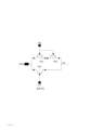
(參考例之資料鎖存電路XDL與本實施方式之資料鎖存電路XDL之比較) 圖15表示參考例之資料鎖存電路XDL之電路圖。比較圖15所示之參考例之資料鎖存電路XDL與圖6所示之本實施方式之資料鎖存電路XDL可知,本實施方式之資料鎖存電路XDL中設置有2個電晶體TN31、TN32,而參考例之資料鎖存電路XDL中僅設置有一個電晶體TN31。於上述參考例之資料鎖存電路XDL之構成之情形時,若連接於電晶體TN31之閘極之通孔、或連接於通孔之配線發生開路故障,則不僅資料鎖存電路XDL之動作會變得不穩定,還會有包含發生了故障之資料鎖存電路XDL之感測放大器單元SAU、及經由匯流排XBUS與資料鎖存電路XDL連接之其他感測放大器單元SAU無法再使用之虞。(Comparison between the data latch circuit XDL of the reference example and the data latch circuit XDL of the present embodiment) FIG. 15 shows a circuit diagram of the data latch circuit XDL of the reference example. Comparing the data latch circuit XDL of the reference example shown in FIG. 15 with the data latch circuit XDL of the present embodiment shown in FIG. , while only one transistor TN31 is provided in the data latch circuit XDL of the reference example. In the case of the configuration of the data latch circuit XDL in the above reference example, if an open fault occurs in the through hole connected to the gate of the transistor TN31 or the wiring connected to the through hole, not only the action of the data latch circuit XDL will be affected. It becomes unstable, and the sense amplifier unit SAU including the failed data latch circuit XDL and other sense amplifier units SAU connected to the data latch circuit XDL via the bus XBUS may become unusable.
詳細而言,製造如圖7所示之半導體記憶裝置2時,在將通孔連接於該電晶體TN31之閘極之步驟、及將配線連接於該通孔之步驟中,通孔或配線有可能發生開路故障。若連接於閘極之通孔或配線發生開路故障,則電晶體TN31之閘極會變成浮動,從而無法控制其閘極電壓。該情形時,電晶體TN31之閘極電壓由於是藉由來自電晶體TN31之附近傳送之鄰接信號之電荷共享而決定,故會變成非常不穩定之電壓。因鄰接信號之狀況會隨時變化,因此最終變得無法控制電晶體TN31之接通/斷開。In detail, when manufacturing the
於資料鎖存電路XDL鎖存有資料之狀態下,電晶體TN13本來必須維持為斷開狀態。但於如上所述般無法控制電晶體TN13之接通/斷開之情形時,即便於鎖存有資料之狀態下,亦有可能發生所謂之通路故障,即電晶體TN13於非預期之時序成為接通狀態。另一方面,當處於鎖存有資料之狀態時,為了使電晶體TP31斷開,而將控制信號XNL設定為高位準,因此電晶體TN13被設定為接通狀態。因此,若電晶體TN13於非預期之時序成為接通狀態,則有匯流排XBUS連接於接地電位節點VSS之虞。即,與具有發生了通路故障之電晶體TN13之資料鎖存電路XDL連接之匯流排XBUS有可能於非預期之時序轉變成接地電位。In the state where data is latched by the data latch circuit XDL, the transistor TN13 must be kept in an off state. However, when the on/off of the transistor TN13 cannot be controlled as described above, even in the state of latching data, the so-called path failure may occur, that is, the transistor TN13 becomes connected state. On the other hand, when the data is latched, in order to turn off the transistor TP31, the control signal XNL is set to a high level, so the transistor TN13 is set to an on state. Therefore, if the transistor TN13 is turned on at an unexpected timing, the bus XBUS may be connected to the ground potential node VSS. That is, there is a possibility that the bus XBUS connected to the data latch circuit XDL having the transistor TN13 in which the path failure occurred turns to the ground potential at an unexpected timing.
如圖5所示,例如複數個感測放大器單元SAU各自之資料鎖存電路XDL0連接於共通之匯流排XBUS。因此,於複數個感測放大器單元SAU中之一個感測放大器單元SAU之資料鎖存電路XDL0發生了電晶體TN13之通路故障之情形時,若欲自未發生通路故障之其他資料鎖存電路XDL0向匯流排XBUS傳送資料時,藉由強行地使匯流排XBUS轉變成接地電位,則有可能無法適當地傳送資料。其結果,不僅是電晶體TN13發生了通路故障之資料鎖存電路XDL無法使用,與其共享匯流排XBUS之所有資料鎖存電路XDL均變得無法使用。As shown in FIG. 5 , for example, the respective data latch circuits XDL0 of the plurality of sense amplifier units SAU are connected to a common bus XBUS. Therefore, when the data latch circuit XDL0 of one sense amplifier unit SAU among the plurality of sense amplifier units SAU has a passage failure of the transistor TN13, if the other data latch circuit XDL0 that does not have a passage failure occurs, When transferring data to the bus XBUS, by forcibly changing the bus XBUS to the ground potential, there is a possibility that the data cannot be transferred properly. As a result, not only the data latch circuit XDL whose path failure occurs in the transistor TN13 becomes unusable, but also all the data latch circuits XDL that share the bus XBUS with it become unusable.
又,與某資料鎖存電路XDL共享匯流排DBUS之所有感測放大器電路SAC0~SAC(m-1)係作為1個整體而加以控制,因此若電晶體TN13發生了通路故障之資料鎖存電路XDL之動作變得不穩定,則與該資料鎖存電路XDL共享匯流排DBUS之所有感測放大器電路SAC0~SAC(m-1)亦有可能變得無法使用。Also, all the sense amplifier circuits SAC0~SAC(m-1) sharing the bus DBUS with a data latch circuit XDL are controlled as a whole, so if the data latch circuit of the transistor TN13 has a path failure If the operation of XDL becomes unstable, all the sense amplifier circuits SAC0˜SAC(m−1) sharing the bus DBUS with the data latch circuit XDL may also become unusable.
鑒於該點,本實施方式之資料鎖存電路XDL如圖6所示,具有2個電晶體TN31、TN32作為與控制信號XTL對應之電晶體。根據該構成,即便其中一電晶體TN31發生了通路故障,只要另一電晶體TN32正常,匯流排XBUS便不會於非預期之時序轉變成接地電位。即,即便電晶體TN31、TN32中之任一者發生了通路故障,亦能藉由正常之另一電晶體確保資料鎖存電路XDL之動作。因此,能提高資料輸入輸出之穩健性。In view of this point, the data latch circuit XDL of this embodiment has two transistors TN31 and TN32 as transistors corresponding to the control signal XTL, as shown in FIG. 6 . According to this configuration, even if one of the transistors TN31 has a path failure, as long as the other transistor TN32 is normal, the bus bar XBUS will not change to the ground potential at an unexpected timing. That is, even if any one of the transistors TN31 and TN32 has a path failure, the other normal transistor can ensure the operation of the data latch circuit XDL. Therefore, the robustness of data input and output can be improved.
(第1變化例) 作為將配線連接於電晶體TN31之通孔V31及電晶體TN32之通孔V32之方法,亦可採用與圖8所示之方法不同之方法。(First Variation) As a method of connecting wiring to the through hole V31 of the transistor TN31 and the through hole V32 of the transistor TN32, a method different from that shown in FIG. 8 may also be used.
例如,如圖16所示,亦可將不同之配線LTG1、LTG2分別連接於電晶體TN31之通孔V31及電晶體TN32之通孔V32。於該構成中,控制信號XTL自定序器25分別向配線LTG1、LTG2輸入。For example, as shown in FIG. 16 , different wiring lines LTG1 and LTG2 may be connected to the through hole V31 of the transistor TN31 and the through hole V32 of the transistor TN32 respectively. In this configuration, the control signal XTL is input from the
或者,如圖17所示,亦可將電晶體TN31之通孔V31與電晶體TN32之通孔V32以於進深方向Y上不重疊之方式配置。於該構成中,將配線LTG1、LTG2分別連接於電晶體TN31之通孔V31及電晶體TN32之通孔V32時,該等配線LTG1、LTG2不會重疊。因此,如圖16所示,無需使配線LTG1、LTG2中之任一者彎曲。於本變化例中,配線LTG1、LTG2相當於個別之信號線。Alternatively, as shown in FIG. 17, the through hole V31 of the transistor TN31 and the through hole V32 of the transistor TN32 may be arranged so as not to overlap in the depth direction Y. In this configuration, when the wirings LTG1 and LTG2 are respectively connected to the through hole V31 of the transistor TN31 and the through hole V32 of the transistor TN32, these wirings LTG1 and LTG2 do not overlap. Therefore, as shown in FIG. 16 , there is no need to bend any of the wiring lines LTG1 , LTG2 . In this modification example, the wiring lines LTG1 and LTG2 correspond to individual signal lines.
(第2變化例) 本變化例之資料鎖存電路XDL具有圖18所示之構成。如圖18所示,該資料鎖存電路XDL中,於匯流排XBUS與節點LAT之間,連接有為P通道型MOS電晶體之2個電晶體TP31、TP32、及為N通道型MOS電晶體之電晶體TN31。電晶體TP31、TP32串聯連接。電晶體TN31與串聯連接之電晶體TP31、TP32並聯連接。根據該構成,即便電晶體TP31、TP32中之任一者發生了故障,亦能藉由正常之另一電晶體確保資料鎖存電路XDL之動作。(Second Variation) The data latch circuit XDL of this variation has the configuration shown in FIG. 18 . As shown in Figure 18, in the data latch circuit XDL, two transistors TP31 and TP32 which are P-channel MOS transistors and an N-channel MOS transistor are connected between the bus XBUS and the node LAT The transistor TN31. Transistors TP31 and TP32 are connected in series. Transistor TN31 is connected in parallel with transistors TP31 and TP32 connected in series. According to this configuration, even if any one of the transistors TP31 and TP32 fails, the operation of the data latch circuit XDL can be ensured by the other normal transistor.
或者,資料鎖存電路XDL亦可具有圖19所示之構成。如圖19所示,該資料鎖存電路XDL中,於匯流排XBUS與節點LAT之間,連接有為CMOS電晶體之2個電晶體TC31、TC32。電晶體TC31具有N通道型MOS電晶體TN31與P通道型MOS電晶體TP31。同樣地,電晶體TC32具有N通道型MOS電晶體TN32與P通道型MOS電晶體TP32。N通道型MOS電晶體TN31、TN32串聯連接。P通道型MOS電晶體TP31、TP32亦串聯連接。Alternatively, the data latch circuit XDL may also have the configuration shown in FIG. 19 . As shown in FIG. 19, in the data latch circuit XDL, two CMOS transistors TC31 and TC32 are connected between the bus XBUS and the node LAT. The transistor TC31 has an N-channel MOS transistor TN31 and a P-channel MOS transistor TP31. Likewise, the transistor TC32 has an N-channel MOS transistor TN32 and a P-channel MOS transistor TP32. N-channel MOS transistors TN31 and TN32 are connected in series. P-channel type MOS transistors TP31 and TP32 are also connected in series.
根據該構成,即便電晶體TC31、TC32中之任一者發生了故障,亦能藉由正常之另一電晶體確保資料鎖存電路XDL之動作。According to this configuration, even if one of the transistors TC31 and TC32 fails, the operation of the data latch circuit XDL can be ensured by the other normal transistor.
(第3變化例) 如圖20所示,於本變化例之資料鎖存電路XDL中,對電晶體TN31、TN32進而串聯連接有為N通道型電晶體之電晶體TN33。根據該構成,即便3個電晶體TN31、TN32、TN33中之1個或2個電晶體發生了故障,亦能藉由剩下之電晶體確保資料鎖存電路XDL之動作。(Third Variation) As shown in FIG. 20, in the data latch circuit XDL of this variation, transistors TN31 and TN32 are further connected in series with transistor TN33 which is an N-channel transistor. According to this configuration, even if one or two of the three transistors TN31, TN32, and TN33 fail, the operation of the data latch circuit XDL can be ensured by the remaining transistors.
再者,N通道型MOS電晶體能以3以上之數多工化。又,亦可並非N通道型MOS電晶體,而是P通道型MOS電晶體以3以上之數多工化。Furthermore, N-channel MOS transistors can be multiplexed with more than 3. In addition, instead of N-channel MOS transistors, P-channel MOS transistors may be multiplexed by the number of 3 or more.
(第4變化例) 本變化例之資料鎖存電路XDL具有圖21所示之構成。如圖21所示,於該資料鎖存電路XDL中,為N通道型電晶體之3個電晶體TN31、TN32、TN33串聯連接。電晶體TN31、TN32之閘極被輸入控制信號XTL。電晶體TN32之閘極被輸入與控制信號XTL不同之控制信號XTLL。於該變化例中,電晶體TN31、TN32、TN33相當於多工化電晶體,電晶體TN31、TN32相當於第1電晶體,電晶體TN33相當於第2電晶體。又,控制信號XTL相當於第1信號,控制信號XTLL相當於第2信號。(Fourth Variation) The data latch circuit XDL of this variation has the configuration shown in FIG. 21 . As shown in FIG. 21, in this data latch circuit XDL, three transistors TN31, TN32, and TN33, which are N-channel transistors, are connected in series. The gate electrodes of the transistors TN31 and TN32 are input with the control signal XTL. A control signal XTLL different from the control signal XTL is input to the gate of the transistor TN32. In this modified example, transistors TN31, TN32, and TN33 correspond to multiplexing transistors, transistors TN31, TN32 correspond to a first transistor, and transistor TN33 corresponds to a second transistor. Also, the control signal XTL corresponds to the first signal, and the control signal XTLL corresponds to the second signal.
又,於半導體記憶裝置2具有如圖8所示之構造之情形時,例如有配線LTG之中間部分P1發生了開路故障時,電晶體TN31、TN32各自之閘極浮動之可能性。該情形時,儘管設置了雙重化之電晶體TN31、TN32,但有電晶體TN31、TN32兩者均發生通路故障之可能性。Also, when the
鑒於該點,若為如圖21所示之構成,則即便電晶體TN31、TN32兩者均發生了通路故障,亦能藉由利用控制信號XTLL控制電晶體TN33之接通/斷開而確保資料鎖存電路XDL之動作。藉此,能進而提高資料輸入輸出之穩健性。In view of this point, with the configuration shown in FIG. 21, even if a path failure occurs in both transistors TN31 and TN32, the data can be secured by controlling the on/off of transistor TN33 by using the control signal XTLL. The operation of the latch circuit XDL. Thereby, the robustness of data input and output can be further improved.
再者,資料鎖存電路XDL亦可具有圖22所示之構成。如圖22所示,於該資料鎖存電路XDL中,電晶體TN31、TN33之閘極被輸入控制信號XTL,電晶體TN32之閘極被輸入不同之控制信號XTLL。於該變化例中,電晶體TN31、TN33相當於第1電晶體,電晶體TN32相當於第2電晶體。Furthermore, the data latch circuit XDL may also have the configuration shown in FIG. 22 . As shown in FIG. 22 , in the data latch circuit XDL, the gates of transistors TN31 and TN33 are input with a control signal XTL, and the gates of transistor TN32 are input with a different control signal XTLL. In this modified example, transistors TN31 and TN33 correspond to the first transistor, and transistor TN32 corresponds to the second transistor.
或者,資料鎖存電路XDL亦可具有圖23所示之構成。如圖23所示,於該資料鎖存電路XDL中,4個電晶體TN31、TN32、TN33、TN34串聯連接。電晶體TN31、TN34之閘極被輸入控制信號XTL,電晶體TN32、TN33之閘極被輸入不同之控制信號XTLL。於該變化例中,電晶體TN31、TN34相當於第1電晶體,電晶體TN32、TN33相當於第2電晶體。Alternatively, the data latch circuit XDL may also have the configuration shown in FIG. 23 . As shown in FIG. 23, in this data latch circuit XDL, four transistors TN31, TN32, TN33, and TN34 are connected in series. The gates of the transistors TN31 and TN34 are input with a control signal XTL, and the gates of the transistors TN32 and TN33 are input with a different control signal XTLL. In this modified example, transistors TN31 and TN34 correspond to the first transistor, and transistors TN32 and TN33 correspond to the second transistor.
若為如圖22及圖23所示之構成,亦能獲得與圖21所示之構成相同或類似之作用及效果。If it is the structure shown in FIG. 22 and FIG. 23, the same or similar action and effect as the structure shown in FIG. 21 can also be obtained.
<其他實施方式> 本發明並非如上所述被具體限定者。<Other Embodiments> The present invention is not specifically limited as described above.
如圖6、圖18~圖23所示,只要半導體記憶裝置2為配置於匯流排XBUS與節點LAT之間之N通道型MOS電晶體及P通道型MOS電晶體中之至少一者多工化即可。As shown in FIG. 6 and FIG. 18 to FIG. 23, as long as the
業者對上述具體例適當施以設計變更而獲得者只要具備本發明之特徵,同樣包含於本發明之範圍內。上述各具體例具備之各要素及其配置、條件、形狀等並不限定於例示者,而可適當變更。上述各具體例具備之各要素只要不存在技術矛盾,便可適當改變組合。Those obtained by suitably modifying the design of the above-mentioned specific examples by the manufacturer are also included in the scope of the present invention as long as they have the characteristics of the present invention. The elements included in each of the above-mentioned specific examples, their arrangement, conditions, shapes, etc. are not limited to those shown in the examples, and can be appropriately changed. As long as there is no technical conflict, the combinations of the various elements included in the above-mentioned specific examples can be appropriately changed.
[相關申請] 本申請享有以日本專利申請2021-154184號(申請日:2021年9月22日)為基礎申請之優先權。本申請藉由參照該基礎申請而包含基礎申請之全部內容。[Related Applications] This application enjoys the priority of the basic application based on Japanese Patent Application No. 2021-154184 (filing date: September 22, 2021). This application incorporates the entire content of the basic application by referring to this basic application.
1:記憶體控制器 2:半導體記憶裝置 11:隨機存取記憶體 12:處理器 13:主機介面 14:錯誤檢測與校正電路 15:記憶體介面 16:內部匯流排 21:記憶單元陣列 22:輸入輸出電路 23:邏輯控制電路 24:暫存器 25:定序器 26:電壓產生電路 27:列解碼器 28:感測放大器 30:輸入輸出用焊墊群 31:邏輯控制用焊墊群 32:電源輸入用端子群 40:半導體基板 220:資料轉換部 221:輸入輸出控制部 520:導電體層 531, 532, 533, 616:配線層 534:記憶孔 539:接觸插塞 611~615:導電體 620~624:接點 BL(BL0, BL1, …, BL(n-1)):位元線 BLC, BLS, BLX, HLL, STB, STL, STI, , SW, XLL, XLI, XNL, XNI, XTL, XTI:控制信號 BLK:塊 C10:電容器 DL(DL0~DL(m-1)), ADL, BDL, CDL, SDL, XDL(XDL0~XDL(m-1)):資料鎖存電路 DBUS, XBUS(XBUS0~XBUS(m-1)):匯流排(資料配線) LAT, COM, SEN, SRC, INV:節點 LTG, LTG1, LTG2:信號線 LT1, LT2, LT3:閘極部 LW1, LW2, LW3:源極・汲極部 MG:記憶單元電晶體之集合 MT(MT0~MT7):記憶單元電晶體 NS:NAND串 PER:周邊電路 SA(SA0~SA(m-1)):感測放大器部 SAC:感測放大器電路 SAU(SAU0~SAU(k-1)):感測放大器單元 SGD0~SGD3, SGS:選擇閘極線 ST1, ST2:選擇電晶體 SL:源極線 SU(SU0~SU3):串單元 TR, TR1~TR14, TRXX:電晶體 TN11~13, TN21, TN31~TN34:N通道型MOS電晶體 TP11~14, TP21, TP31, TP32:P通道型MOS電晶體 VDD:電源電位節點 VSS:接地電位節點 WL0~WL7:字元線 XIV:反相器電路(資料保持部) 1: Memory controller 2: Semiconductor memory device 11: Random Access Memory 12: Processor 13: Host interface 14: Error detection and correction circuit 15: Memory interface 16: Internal busbar 21: memory cell array 22: Input and output circuit 23: Logic control circuit 24: scratchpad 25: Sequencer 26: Voltage generating circuit 27: column decoder 28: Sense amplifier 30: pad group for input and output 31: pad group for logic control 32: Terminal group for power input 40: Semiconductor substrate 220: Data conversion department 221: Input and output control unit 520: conductor layer 531, 532, 533, 616: wiring layer 534: memory hole 539: contact plug 611~615: Conductor 620~624: contacts BL(BL0, BL1, …, BL(n-1)): bit line BLC, BLS, BLX, HLL, STB, STL, STI, , SW, XLL, XLI, XNL, XNI, XTL, XTI: Control signals BLK: block C10: Capacitor DL(DL0~DL(m-1)), ADL, BDL, CDL, SDL, XDL(XDL0~XDL(m-1)): data latch circuit DBUS, XBUS(XBUS0~XBUS(m-1)): busbar (data wiring) LAT, COM, SEN, SRC, INV: nodes LTG, LTG1, LTG2: Signal lines LT1, LT2, LT3: gate part LW1, LW2, LW3: Source and sink parts MG: A collection of memory cell transistors MT(MT0~MT7): memory unit transistor NS: NAND string PER: peripheral circuit SA(SA0~SA(m-1)): Sense Amplifier Section SAC: sense amplifier circuit SAU(SAU0~SAU(k-1)): Sense Amplifier Unit SGD0~SGD3, SGS: select gate line ST1, ST2: select transistor SL: source line SU(SU0~SU3): string unit TR, TR1~TR14, TRXX: Transistor TN11~13, TN21, TN31~TN34: N-channel MOS transistors TP11~14, TP21, TP31, TP32: P-channel MOS transistors VDD: power supply potential node VSS: ground potential node WL0~WL7: character line XIV: Inverter circuit (data holding part)
圖1係表示實施方式之記憶系統之概略構成之方塊圖。 圖2係表示實施方式之半導體記憶裝置之概略構成之方塊圖。 圖3係表示實施方式之半導體記憶裝置之構成之電路圖。 圖4係表示實施方式之感測放大器單元之概略構成之方塊圖。 圖5係表示實施方式之感測放大器及輸入輸出電路之概略構成之方塊圖。 圖6係表示實施方式之資料鎖存電路之構成之電路圖。 圖7係表示實施方式之半導體記憶裝置之剖面構造之剖視圖。 圖8係模式性表示實施方式之半導體記憶裝置之資料鎖存電路周邊的平面構造之圖。 圖9係模式性表示參考例之半導體記憶裝置之資料鎖存電路周邊的平面構造之圖。 圖10係表示實施方式之資料鎖存電路之動作例之電路圖。 圖11係表示實施方式之資料鎖存電路之動作例之電路圖。 圖12係表示實施方式之資料鎖存電路之動作例之電路圖。 圖13係表示實施方式之資料鎖存電路之動作例之電路圖。 圖14係表示實施方式之資料鎖存電路之動作例之電路圖。 圖15係表示參考例之資料鎖存電路之構成之電路圖。 圖16係模式性表示第1變化例之半導體記憶裝置之資料鎖存電路周邊的平面構造之圖。 圖17係模式性表示第1變化例之半導體記憶裝置之資料鎖存電路周邊的平面構造之圖。 圖18係表示第2變化例之資料鎖存電路之構成的一部分之電路圖。 圖19係表示第2變化例之資料鎖存電路之構成的一部分之電路圖。 圖20係表示第3變化例之資料鎖存電路之構成的一部分之電路圖。 圖21係表示第4變化例之資料鎖存電路之構成的一部分之電路圖。 圖22係表示第4變化例之資料鎖存電路之構成的一部分之電路圖。 圖23係表示第4變化例之資料鎖存電路之構成的一部分之電路圖。FIG. 1 is a block diagram showing a schematic configuration of a memory system according to an embodiment. FIG. 2 is a block diagram showing a schematic configuration of a semiconductor memory device according to an embodiment. Fig. 3 is a circuit diagram showing the configuration of the semiconductor memory device of the embodiment. FIG. 4 is a block diagram showing a schematic configuration of the sense amplifier unit of the embodiment. FIG. 5 is a block diagram showing a schematic configuration of a sense amplifier and an input/output circuit of the embodiment. Fig. 6 is a circuit diagram showing the configuration of the data latch circuit of the embodiment. FIG. 7 is a cross-sectional view showing a cross-sectional structure of a semiconductor memory device according to an embodiment. FIG. 8 is a diagram schematically showing the planar structure around the data latch circuit of the semiconductor memory device according to the embodiment. FIG. 9 is a diagram schematically showing the planar structure around the data latch circuit of the semiconductor memory device of the reference example. Fig. 10 is a circuit diagram showing an example of the operation of the data latch circuit of the embodiment. Fig. 11 is a circuit diagram showing an example of the operation of the data latch circuit of the embodiment. Fig. 12 is a circuit diagram showing an example of the operation of the data latch circuit of the embodiment. Fig. 13 is a circuit diagram showing an example of the operation of the data latch circuit of the embodiment. FIG. 14 is a circuit diagram showing an example of the operation of the data latch circuit of the embodiment. Fig. 15 is a circuit diagram showing the configuration of the data latch circuit of the reference example. Fig. 16 is a diagram schematically showing the planar structure around the data latch circuit of the semiconductor memory device of the first variation. Fig. 17 is a diagram schematically showing the planar structure around the data latch circuit of the semiconductor memory device of the first variation. Fig. 18 is a circuit diagram showing a part of the constitution of the data latch circuit of the second modification. Fig. 19 is a circuit diagram showing a part of the composition of the data latch circuit of the second modification. Fig. 20 is a circuit diagram showing a part of the constitution of the data latch circuit of the third modification. Fig. 21 is a circuit diagram showing a part of the constitution of the data latch circuit of the fourth modification. Fig. 22 is a circuit diagram showing a part of the constitution of the data latch circuit of the fourth modification. Fig. 23 is a circuit diagram showing a part of the constitution of the data latch circuit of the fourth modification.
DBUS, XBUS:匯流排(資料配線) LAT, INV:節點 TN11~13, TN21, TN31, TN32:N通道型MOS電晶體 TP11~14, TP21, TP31:P通道型MOS電晶體 VDD:電源電位節點 VSS:接地電位節點 XDL:資料鎖存電路 XLL, XLI, XNL, XNI, XTL, XTI:控制信號 XIV:反相器電路(資料保持部) DBUS, XBUS: busbar (data wiring) LAT, INV: node TN11~13, TN21, TN31, TN32: N-channel MOS transistors TP11~14, TP21, TP31: P-channel MOS transistors VDD: power supply potential node VSS: ground potential node XDL: data latch circuit XLL, XLI, XNL, XNI, XTL, XTI: control signals XIV: Inverter circuit (data holding part)
Claims (5)
Applications Claiming Priority (2)
| Application Number | Priority Date | Filing Date | Title |
|---|---|---|---|
| JP2021154184A JP2023045647A (en) | 2021-09-22 | 2021-09-22 | Semiconductor memory device |
| JP2021-154184 | 2021-09-22 |
Publications (2)
| Publication Number | Publication Date |
|---|---|
| TW202314716A TW202314716A (en) | 2023-04-01 |
| TWI802199B true TWI802199B (en) | 2023-05-11 |
Family
ID=85572133
Family Applications (2)
| Application Number | Title | Priority Date | Filing Date |
|---|---|---|---|
| TW111100118A TWI802199B (en) | 2021-09-22 | 2022-01-03 | semiconductor memory device |
| TW112113004A TWI896958B (en) | 2021-09-22 | 2022-01-03 | semiconductor memory devices |
Family Applications After (1)
| Application Number | Title | Priority Date | Filing Date |
|---|---|---|---|
| TW112113004A TWI896958B (en) | 2021-09-22 | 2022-01-03 | semiconductor memory devices |
Country Status (4)
| Country | Link |
|---|---|
| US (1) | US11894095B2 (en) |
| JP (1) | JP2023045647A (en) |
| CN (1) | CN115938457B (en) |
| TW (2) | TWI802199B (en) |
Families Citing this family (3)
| Publication number | Priority date | Publication date | Assignee | Title |
|---|---|---|---|---|
| JP2024135839A (en) * | 2023-03-23 | 2024-10-04 | キオクシア株式会社 | Semiconductor memory device |
| US20250240949A1 (en) * | 2024-01-18 | 2025-07-24 | Taiwan Semiconductor Manufacturing Company, Ltd. | 3d memory array archetecture and method of fabricating the same |
| JP2025144346A (en) * | 2024-03-19 | 2025-10-02 | キオクシア株式会社 | Semiconductor memory device, memory system |
Citations (4)
| Publication number | Priority date | Publication date | Assignee | Title |
|---|---|---|---|---|
| US6590802B2 (en) * | 2001-11-13 | 2003-07-08 | Mitsubishi Denki Kabushiki Kaisha | Semiconductor storage apparatus |
| US9082640B2 (en) * | 2012-09-06 | 2015-07-14 | Kabushiki Kaisha Toshiba | Pass gate and semiconductor storage device having the same |
| TWI521522B (en) * | 2013-03-21 | 2016-02-11 | Toshiba Kk | Nonvolatile semiconductor memory device and its control method |
| TW201905920A (en) * | 2017-06-22 | 2019-02-01 | 蕭志成 | Static Random Access Memory (SRAM) Cell |
Family Cites Families (16)
| Publication number | Priority date | Publication date | Assignee | Title |
|---|---|---|---|---|
| US5357462A (en) * | 1991-09-24 | 1994-10-18 | Kabushiki Kaisha Toshiba | Electrically erasable and programmable non-volatile semiconductor memory with automatic write-verify controller |
| JPH07202131A (en) * | 1993-12-28 | 1995-08-04 | Mitsubishi Electric Corp | Semiconductor integrated circuit |
| JP2007172715A (en) * | 2005-12-20 | 2007-07-05 | Fujitsu Ltd | Semiconductor memory device and control method thereof |
| JP2010160865A (en) * | 2009-01-09 | 2010-07-22 | Toshiba Corp | Semiconductor memory device and method of driving semiconductor memory device |
| JP5282607B2 (en) * | 2009-02-26 | 2013-09-04 | ソニー株式会社 | Resistance change type memory device and operation method thereof |
| JP2011129176A (en) | 2009-12-15 | 2011-06-30 | Toshiba Corp | Nonvolatile semiconductor memory device |
| CN106575525B (en) * | 2014-08-28 | 2020-09-25 | 东芝存储器株式会社 | Semiconductor memory device with a plurality of memory cells |
| JP6753846B2 (en) * | 2014-10-21 | 2020-09-09 | サノフィ−アベンティス・ドイチュラント・ゲゼルシャフト・ミット・ベシュレンクテル・ハフツング | Recording dose data from drug injection devices using optical character recognition |
| JP2016162475A (en) * | 2015-03-04 | 2016-09-05 | 株式会社東芝 | Semiconductor memory device |
| US9704572B2 (en) | 2015-03-20 | 2017-07-11 | Sandisk Technologies Llc | Sense amplifier with integrating capacitor and methods of operation |
| JP6581019B2 (en) * | 2016-03-02 | 2019-09-25 | 東芝メモリ株式会社 | Semiconductor memory device |
| JP6645933B2 (en) | 2016-08-19 | 2020-02-14 | キオクシア株式会社 | Data latch circuit and semiconductor device |
| CN107424644B (en) * | 2017-08-02 | 2020-06-09 | 上海兆芯集成电路有限公司 | Reading circuit and reading method |
| JP2019036375A (en) * | 2017-08-17 | 2019-03-07 | 東芝メモリ株式会社 | Semiconductor memory device |
| JP2020042889A (en) * | 2018-09-13 | 2020-03-19 | キオクシア株式会社 | Semiconductor storage device |
| KR102765578B1 (en) * | 2020-01-14 | 2025-02-12 | 에스케이하이닉스 주식회사 | Semiconductor memory device having page buffer |
-
2021
- 2021-09-22 JP JP2021154184A patent/JP2023045647A/en active Pending
-
2022
- 2022-01-03 TW TW111100118A patent/TWI802199B/en active
- 2022-01-03 TW TW112113004A patent/TWI896958B/en active
- 2022-01-25 CN CN202210086608.5A patent/CN115938457B/en active Active
- 2022-03-02 US US17/685,230 patent/US11894095B2/en active Active
Patent Citations (4)
| Publication number | Priority date | Publication date | Assignee | Title |
|---|---|---|---|---|
| US6590802B2 (en) * | 2001-11-13 | 2003-07-08 | Mitsubishi Denki Kabushiki Kaisha | Semiconductor storage apparatus |
| US9082640B2 (en) * | 2012-09-06 | 2015-07-14 | Kabushiki Kaisha Toshiba | Pass gate and semiconductor storage device having the same |
| TWI521522B (en) * | 2013-03-21 | 2016-02-11 | Toshiba Kk | Nonvolatile semiconductor memory device and its control method |
| TW201905920A (en) * | 2017-06-22 | 2019-02-01 | 蕭志成 | Static Random Access Memory (SRAM) Cell |
Also Published As
| Publication number | Publication date |
|---|---|
| CN115938457A (en) | 2023-04-07 |
| JP2023045647A (en) | 2023-04-03 |
| TWI896958B (en) | 2025-09-11 |
| US20230087689A1 (en) | 2023-03-23 |
| TW202329119A (en) | 2023-07-16 |
| TW202314716A (en) | 2023-04-01 |
| CN115938457B (en) | 2026-03-27 |
| US11894095B2 (en) | 2024-02-06 |
Similar Documents
| Publication | Publication Date | Title |
|---|---|---|
| US10319416B2 (en) | Memory device including page buffers | |
| TWI644316B (en) | Semiconductor storage device | |
| CN115938457B (en) | Semiconductor memory devices | |
| CN115620777B (en) | Semiconductor memory devices | |
| TWI710119B (en) | Semiconductor memory device | |
| JP2022142226A (en) | semiconductor storage device | |
| US10861865B2 (en) | Semiconductor storage device | |
| TWI828162B (en) | semiconductor memory device | |
| US12211561B2 (en) | Semiconductor storage device acquiring voltage from dummy pillars | |
| US12626735B2 (en) | Semiconductor memory device with voltage-controlled data latch node | |
| TWI919676B (en) | Semiconductor memory devices | |
| TW379328B (en) | Column decoding circuit of flash memory having separated character lines | |
| TW202341157A (en) | semiconductor memory device | |
| JP2023086292A (en) | semiconductor storage device | |
| JP2022143283A (en) | semiconductor storage device | |
| US12525310B2 (en) | Semiconductor device and semiconductor storage device configured for operation in a normal mode and two test modes | |
| US20250299746A1 (en) | Semiconductor storage device | |
| US12580027B2 (en) | Semiconductor storage device | |
| US20260088107A1 (en) | Semiconductor device | |
| TWI539465B (en) | Semiconductor storing device and redundancy method thereof | |
| JP4833073B2 (en) | Semiconductor device and data reading method | |
| CN120673816A (en) | Semiconductor memory device and memory system |