TWI804580B - Precursor film, substrate with a layer to be plated, conductive film, touch panel sensor, touch panel, a method for producing a conductive film, and a composition for forming a layer to be plated - Google Patents
Precursor film, substrate with a layer to be plated, conductive film, touch panel sensor, touch panel, a method for producing a conductive film, and a composition for forming a layer to be plated Download PDFInfo
- Publication number
- TWI804580B TWI804580B TW108105674A TW108105674A TWI804580B TW I804580 B TWI804580 B TW I804580B TW 108105674 A TW108105674 A TW 108105674A TW 108105674 A TW108105674 A TW 108105674A TW I804580 B TWI804580 B TW I804580B
- Authority
- TW
- Taiwan
- Prior art keywords
- layer
- precursor
- plated
- substrate
- group
- Prior art date
Links
Images


Classifications
-
- B—PERFORMING OPERATIONS; TRANSPORTING
- B32—LAYERED PRODUCTS
- B32B—LAYERED PRODUCTS, i.e. PRODUCTS BUILT-UP OF STRATA OF FLAT OR NON-FLAT, e.g. CELLULAR OR HONEYCOMB, FORM
- B32B17/00—Layered products essentially comprising sheet glass, or glass, slag, or like fibres
- B32B17/06—Layered products essentially comprising sheet glass, or glass, slag, or like fibres comprising glass as the main or only constituent of a layer, next to another layer of a specific material
- B32B17/10—Layered products essentially comprising sheet glass, or glass, slag, or like fibres comprising glass as the main or only constituent of a layer, next to another layer of a specific material of synthetic resin
-
- B—PERFORMING OPERATIONS; TRANSPORTING
- B01—PHYSICAL OR CHEMICAL PROCESSES OR APPARATUS IN GENERAL
- B01J—CHEMICAL OR PHYSICAL PROCESSES, e.g. CATALYSIS OR COLLOID CHEMISTRY; THEIR RELEVANT APPARATUS
- B01J31/00—Catalysts comprising hydrides, coordination complexes or organic compounds
- B01J31/02—Catalysts comprising hydrides, coordination complexes or organic compounds containing organic compounds or metal hydrides
- B01J31/0201—Oxygen-containing compounds
- B01J31/0205—Oxygen-containing compounds comprising carbonyl groups or oxygen-containing derivatives, e.g. acetals, ketals, cyclic peroxides
-
- B—PERFORMING OPERATIONS; TRANSPORTING
- B32—LAYERED PRODUCTS
- B32B—LAYERED PRODUCTS, i.e. PRODUCTS BUILT-UP OF STRATA OF FLAT OR NON-FLAT, e.g. CELLULAR OR HONEYCOMB, FORM
- B32B27/00—Layered products comprising a layer of synthetic resin
- B32B27/36—Layered products comprising a layer of synthetic resin comprising polyesters
-
- C—CHEMISTRY; METALLURGY
- C08—ORGANIC MACROMOLECULAR COMPOUNDS; THEIR PREPARATION OR CHEMICAL WORKING-UP; COMPOSITIONS BASED THEREON
- C08F—MACROMOLECULAR COMPOUNDS OBTAINED BY REACTIONS ONLY INVOLVING CARBON-TO-CARBON UNSATURATED BONDS
- C08F2/00—Processes of polymerisation
- C08F2/44—Polymerisation in the presence of compounding ingredients, e.g. plasticisers, dyestuffs, fillers
-
- C—CHEMISTRY; METALLURGY
- C08—ORGANIC MACROMOLECULAR COMPOUNDS; THEIR PREPARATION OR CHEMICAL WORKING-UP; COMPOSITIONS BASED THEREON
- C08F—MACROMOLECULAR COMPOUNDS OBTAINED BY REACTIONS ONLY INVOLVING CARBON-TO-CARBON UNSATURATED BONDS
- C08F299/00—Macromolecular compounds obtained by interreacting polymers involving only carbon-to-carbon unsaturated bond reactions, in the absence of non-macromolecular monomers
- C08F299/02—Macromolecular compounds obtained by interreacting polymers involving only carbon-to-carbon unsaturated bond reactions, in the absence of non-macromolecular monomers from unsaturated polycondensates
-
- C—CHEMISTRY; METALLURGY
- C23—COATING METALLIC MATERIAL; COATING MATERIAL WITH METALLIC MATERIAL; CHEMICAL SURFACE TREATMENT; DIFFUSION TREATMENT OF METALLIC MATERIAL; COATING BY VACUUM EVAPORATION, BY SPUTTERING, BY ION IMPLANTATION OR BY CHEMICAL VAPOUR DEPOSITION, IN GENERAL; INHIBITING CORROSION OF METALLIC MATERIAL OR INCRUSTATION IN GENERAL
- C23C—COATING METALLIC MATERIAL; COATING MATERIAL WITH METALLIC MATERIAL; SURFACE TREATMENT OF METALLIC MATERIAL BY DIFFUSION INTO THE SURFACE, BY CHEMICAL CONVERSION OR SUBSTITUTION; COATING BY VACUUM EVAPORATION, BY SPUTTERING, BY ION IMPLANTATION OR BY CHEMICAL VAPOUR DEPOSITION, IN GENERAL
- C23C18/00—Chemical coating by decomposition of either liquid compounds or solutions of the coating forming compounds, without leaving reaction products of surface material in the coating; Contact plating
- C23C18/16—Chemical coating by decomposition of either liquid compounds or solutions of the coating forming compounds, without leaving reaction products of surface material in the coating; Contact plating by reduction or substitution, e.g. electroless plating
- C23C18/18—Pretreatment of the material to be coated
-
- C—CHEMISTRY; METALLURGY
- C23—COATING METALLIC MATERIAL; COATING MATERIAL WITH METALLIC MATERIAL; CHEMICAL SURFACE TREATMENT; DIFFUSION TREATMENT OF METALLIC MATERIAL; COATING BY VACUUM EVAPORATION, BY SPUTTERING, BY ION IMPLANTATION OR BY CHEMICAL VAPOUR DEPOSITION, IN GENERAL; INHIBITING CORROSION OF METALLIC MATERIAL OR INCRUSTATION IN GENERAL
- C23C—COATING METALLIC MATERIAL; COATING MATERIAL WITH METALLIC MATERIAL; SURFACE TREATMENT OF METALLIC MATERIAL BY DIFFUSION INTO THE SURFACE, BY CHEMICAL CONVERSION OR SUBSTITUTION; COATING BY VACUUM EVAPORATION, BY SPUTTERING, BY ION IMPLANTATION OR BY CHEMICAL VAPOUR DEPOSITION, IN GENERAL
- C23C18/00—Chemical coating by decomposition of either liquid compounds or solutions of the coating forming compounds, without leaving reaction products of surface material in the coating; Contact plating
- C23C18/16—Chemical coating by decomposition of either liquid compounds or solutions of the coating forming compounds, without leaving reaction products of surface material in the coating; Contact plating by reduction or substitution, e.g. electroless plating
- C23C18/31—Coating with metals
-
- G—PHYSICS
- G02—OPTICS
- G02B—OPTICAL ELEMENTS, SYSTEMS OR APPARATUS
- G02B1/00—Optical elements characterised by the material of which they are made; Optical coatings for optical elements
- G02B1/10—Optical coatings produced by application to, or surface treatment of, optical elements
- G02B1/16—Optical coatings produced by application to, or surface treatment of, optical elements having an anti-static effect, e.g. electrically conducting coatings
-
- G—PHYSICS
- G06—COMPUTING OR CALCULATING; COUNTING
- G06F—ELECTRIC DIGITAL DATA PROCESSING
- G06F3/00—Input arrangements for transferring data to be processed into a form capable of being handled by the computer; Output arrangements for transferring data from processing unit to output unit, e.g. interface arrangements
- G06F3/01—Input arrangements or combined input and output arrangements for interaction between user and computer
- G06F3/03—Arrangements for converting the position or the displacement of a member into a coded form
- G06F3/041—Digitisers, e.g. for touch screens or touch pads, characterised by the transducing means
- G06F3/044—Digitisers, e.g. for touch screens or touch pads, characterised by the transducing means by capacitive means
-
- G—PHYSICS
- G06—COMPUTING OR CALCULATING; COUNTING
- G06F—ELECTRIC DIGITAL DATA PROCESSING
- G06F3/00—Input arrangements for transferring data to be processed into a form capable of being handled by the computer; Output arrangements for transferring data from processing unit to output unit, e.g. interface arrangements
- G06F3/01—Input arrangements or combined input and output arrangements for interaction between user and computer
- G06F3/03—Arrangements for converting the position or the displacement of a member into a coded form
- G06F3/041—Digitisers, e.g. for touch screens or touch pads, characterised by the transducing means
- G06F3/044—Digitisers, e.g. for touch screens or touch pads, characterised by the transducing means by capacitive means
- G06F3/0443—Digitisers, e.g. for touch screens or touch pads, characterised by the transducing means by capacitive means using a single layer of sensing electrodes
-
- H—ELECTRICITY
- H01—ELECTRIC ELEMENTS
- H01B—CABLES; CONDUCTORS; INSULATORS; SELECTION OF MATERIALS FOR THEIR CONDUCTIVE, INSULATING OR DIELECTRIC PROPERTIES
- H01B13/00—Apparatus or processes specially adapted for manufacturing conductors or cables
-
- H—ELECTRICITY
- H01—ELECTRIC ELEMENTS
- H01B—CABLES; CONDUCTORS; INSULATORS; SELECTION OF MATERIALS FOR THEIR CONDUCTIVE, INSULATING OR DIELECTRIC PROPERTIES
- H01B5/00—Non-insulated conductors or conductive bodies characterised by their form
- H01B5/14—Non-insulated conductors or conductive bodies characterised by their form comprising conductive layers or films on insulating-supports
-
- G—PHYSICS
- G06—COMPUTING OR CALCULATING; COUNTING
- G06F—ELECTRIC DIGITAL DATA PROCESSING
- G06F2203/00—Indexing scheme relating to G06F3/00 - G06F3/048
- G06F2203/041—Indexing scheme relating to G06F3/041 - G06F3/045
- G06F2203/04103—Manufacturing, i.e. details related to manufacturing processes specially suited for touch sensitive devices
-
- G—PHYSICS
- G06—COMPUTING OR CALCULATING; COUNTING
- G06F—ELECTRIC DIGITAL DATA PROCESSING
- G06F2203/00—Indexing scheme relating to G06F3/00 - G06F3/048
- G06F2203/041—Indexing scheme relating to G06F3/041 - G06F3/045
- G06F2203/04112—Electrode mesh in capacitive digitiser: electrode for touch sensing is formed of a mesh of very fine, normally metallic, interconnected lines that are almost invisible to see. This provides a quite large but transparent electrode surface, without need for ITO or similar transparent conductive material
Landscapes
- Chemical & Material Sciences (AREA)
- Engineering & Computer Science (AREA)
- Chemical Kinetics & Catalysis (AREA)
- Organic Chemistry (AREA)
- Physics & Mathematics (AREA)
- General Engineering & Computer Science (AREA)
- Theoretical Computer Science (AREA)
- General Physics & Mathematics (AREA)
- Materials Engineering (AREA)
- Human Computer Interaction (AREA)
- Mechanical Engineering (AREA)
- Polymers & Plastics (AREA)
- Medicinal Chemistry (AREA)
- Health & Medical Sciences (AREA)
- Metallurgy (AREA)
- General Chemical & Material Sciences (AREA)
- Optics & Photonics (AREA)
- Manufacturing & Machinery (AREA)
- Chemically Coating (AREA)
- Laminated Bodies (AREA)
- Addition Polymer Or Copolymer, Post-Treatments, Or Chemical Modifications (AREA)
Abstract
本發明提供一種前驅物薄膜,其用於製造導電性薄膜,該前驅物薄膜包括基板、配置在基板上之底漆層及配置在底漆層上之被鍍層前驅物層,被鍍層前驅物層包含2官能自由基聚合性單體和具有與電鍍觸媒或其前驅物相互作用之官能團之聚合物,2官能自由基聚合性單體中連結2個自由基聚合性基團之連結鏈的主鏈的原子數為25個~100個。The invention provides a precursor thin film, which is used to manufacture a conductive thin film. The precursor thin film includes a substrate, a primer layer disposed on the substrate, and a plated precursor layer disposed on the primer layer, and the plated precursor layer A polymer comprising a bifunctional radically polymerizable monomer and a functional group that interacts with an electroplating catalyst or its precursor, the main chain linking two radically polymerizable groups in the bifunctional radically polymerizable monomer The number of atoms in the chain is 25 to 100.
Description
本發明係有關一種前驅物薄膜、附被鍍層基板、導電性薄膜、觸控面板感測器、觸控面板、導電性薄膜的製造方法及被鍍層形成用組成物。The present invention relates to a precursor film, a plated substrate, a conductive film, a touch panel sensor, a touch panel, a manufacturing method of the conductive film, and a composition for forming a plated layer.
於基板上配置有金屬層(較佳為圖案狀金屬層)之導電性薄膜(附金屬層基板)使用於各種用途中。例如,近年來隨著針對行動電話或便攜式遊戲機等的觸控面板的搭載率的上升,能夠進行多點檢測之電容式觸控感測器用導電性薄膜的需求快速擴大。 導電性薄膜的製造方法中提出有各種方案。A conductive thin film (substrate with a metal layer) having a metal layer (preferably a patterned metal layer) disposed on a substrate is used in various applications. For example, in recent years, the demand for conductive films for capacitive touch sensors capable of multi-point detection has rapidly expanded as the mounting rate of touch panels for mobile phones and portable game machines has increased. Various proposals have been made for the production method of the conductive thin film.
例如,專利文獻1中記載有一種具有基板和配置在基板上之被鍍層之附被鍍層基板(申請專利範圍第1、7及8)、包括該附被鍍層基板和配置在附被鍍層基板中的被鍍層上之金屬層之導電性薄膜(申請專利範圍第11),該附被鍍層基板中,被鍍層使包含選自包括具有聚氧化烯基之多官能丙烯醯胺及具有聚氧化烯基之多官能甲基丙烯醯胺之群組中之醯胺化合物、具有與電鍍觸媒或其前驅物相互作用之官能團之聚合物之被鍍層形成用組成物硬化而成。 [先前技術文獻] [專利文獻]For example, Patent Document 1 describes a coated substrate having a substrate and a coated layer arranged on the substrate (patent claims Nos. 1, 7, and 8), including the coated substrate and the coated substrate disposed on the coated substrate. Conductive thin film of the metal layer on the plated layer (patent scope No. 11), in the plated substrate, the plated layer is made of polyfunctional acrylamide with polyoxyalkylene group and polyoxyalkylene group Amide compounds in the group of polyfunctional methacrylamides, polymers with functional groups interacting with electroplating catalysts or their precursors are formed by hardening the coating-forming composition. [Prior Art Literature] [Patent Document]
[專利文獻1]國際公開第2018/034291號[Patent Document 1] International Publication No. 2018/034291
另一方面,最近要求具有三維形狀之導電性薄膜。 例如,為了進一步提高操作性,要求觸控面為曲面等三維形狀的觸控面板,且該種觸控面板中所含有之觸控面板感測器使用具有三維形狀之導電性薄膜。On the other hand, recently, a conductive thin film having a three-dimensional shape is required. For example, in order to further improve operability, a touch panel with a three-dimensional shape such as a curved surface is required, and a touch panel sensor contained in such a touch panel uses a conductive film with a three-dimensional shape.
進而,作為導電性薄膜的基板,要求使用聚對苯二甲酸乙二醇酯薄膜或聚丙烯薄膜等由玻璃化轉變溫度比以往低之原材料組成之薄膜,於比以往的成形溫度更低的低溫下形成為三維形狀。Furthermore, as the substrate of the conductive film, it is required to use a film composed of a material with a glass transition temperature lower than the conventional one, such as a polyethylene terephthalate film or a polypropylene film, at a lower temperature than the conventional forming temperature. The bottom is formed into a three-dimensional shape.
本發明人等欲使用專利文獻1中所記載之附被鍍層基板,以比以往更低的低溫成形而製造具有三維形狀之導電性薄膜。然而,被鍍層的延伸性不夠充分,且很難使被鍍層變形為所希望的形狀。The inventors of the present invention intend to use the plated substrate described in Patent Document 1 to manufacture a conductive thin film having a three-dimensional shape by molding at a lower temperature than conventionally. However, the extensibility of the layer to be plated is not sufficient, and it is difficult to deform the layer to be plated into a desired shape.
本發明的課題為,鑑於上述情況,提供一種即使於比以往更低的低溫下成形的情況下,使被鍍層前驅物硬化而成之被鍍層的延伸性優異之用於製造導電性薄膜之前驅物薄膜。The object of the present invention is to provide a precursor for producing a conductive thin film which is excellent in extensibility of a coating to be coated formed by hardening the coating to be coated precursor even when molding at a lower temperature than conventional ones. object film.
又,本發明的課題亦為提供一種附被鍍層基板、導電性薄膜、觸控面板感測器、觸控面板、導電性薄膜的製造方法及被鍍層形成用組成物。Furthermore, the object of the present invention is also to provide a substrate with a plated layer, a conductive film, a touch panel sensor, a touch panel, a method for manufacturing the conductive film, and a composition for forming a plated layer.
本發明人對上述課題進行深入研究之結果,發現藉由使用具有特定的連結鏈長之2官能自由基聚合性單體和具有與電鍍觸媒或其前驅物相互作用之官能團之聚合物能夠解決上述課題。 亦即,本發明人發現藉由以下結構能夠解決上述課題。As a result of intensive research by the present inventors on the above-mentioned problems, it was found that the solution can be solved by using a bifunctional radically polymerizable monomer having a specific chain length and a polymer having a functional group that interacts with an electroplating catalyst or its precursor. the above subjects. That is, the present inventors found that the above-mentioned problems can be solved by the following structure.
[1]一種前驅物薄膜,其用於製造導電性薄膜,其中
上述前驅物薄膜包括基板、配置在上述基板上之底漆層及配置在上述底漆層上之被鍍層前驅物層,
上述被鍍層前驅物層包含2官能自由基聚合性單體和具有與電鍍觸媒或其前驅物相互作用之官能團之聚合物,
上述2官能自由基聚合性單體中連結2個自由基聚合性基團之連結鏈的主鏈的原子數為25個~100個。
[2]如上述[1]所述之前驅物薄膜,其中
上述2官能自由基聚合性單體的自由基聚合性基團選自包括丙烯醯氧基、甲基丙烯醯氧基、丙烯醯胺基及甲基丙烯醯胺基之群組。
[3]如上述[1]或[2]所述之前驅物薄膜,其中
上述2官能自由基聚合性單體具有聚氧化烯基。
[4]如上述[1]至[3]中任一項所述之前驅物薄膜,其中
上述2官能自由基聚合性單體係由式(100)表示之化合物。
[化1]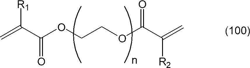
[15]一種導電性薄膜的製造方法,其包括對上述[1]至[8]中任一項所述之前驅物薄膜進行曝光之曝光製程、對經曝光之上述薄膜進行顯影之顯影製程、對經顯影之上述薄膜進行加熱成形之成形製程及對所成形之上述薄膜進行電鍍之電鍍製程。 [16]如上述[15]所述之導電性薄膜的製造方法,其中 於上述成形製程中,於60℃~120℃下進行加熱成形。 [17]如上述[15]或[16]所述之導電性薄膜的製造方法,其中 於上述顯影製程中,用鹼性水溶液清洗經曝光之前驅物薄膜,接著用水進行清洗。[15] A method for producing a conductive film, comprising an exposure process for exposing the precursor film described in any one of [1] to [8] above, a development process for developing the exposed film, A forming process of thermoforming the developed film and an electroplating process of electroplating the formed film. [16] The method for producing a conductive thin film according to the above [15], wherein In the above forming process, heat forming is carried out at 60° C. to 120° C. [17] The method for producing a conductive thin film according to the above [15] or [16], wherein In the above-mentioned development process, the pre-exposed precursor film is washed with an alkaline aqueous solution, and then washed with water.
[18]一種被鍍層形成用組成物,其包括2官能自由基聚合性單體和具有與電鍍觸媒或其前驅物相互作用之官能團之聚合物,
上述2官能自由基聚合性單體中連結2個自由基聚合性基團之連結鏈的主鏈的原子數為25個~100個。
[19]如上述[18]所述之被鍍層形成用組成物,其中
上述2官能自由基聚合性單體的自由基聚合性基團選自包括丙烯醯氧基、甲基丙烯醯氧基、丙烯醯胺基及甲基丙烯醯胺基之群組。
[20]如上述[18]或[19]所述之被鍍層形成用組成物,其中
上述2官能自由基聚合性單體具有聚氧化烯基。
[21]如上述[18]至[20]中任一項所述之被鍍層形成用組成物,其中
上述2官能自由基聚合性單體係由式(100)表示之化合物。
[化2]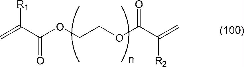
依本發明,能夠提供一種即使於比以往更低的低溫下成形的情況下,使被鍍層前驅物硬化而成之被鍍層的延伸性優異之用於製造導電性薄膜之前驅物薄膜。According to the present invention, it is possible to provide a precursor thin film for the production of a conductive thin film which is excellent in extensibility of the coating to be coated formed by curing the coating to be coated precursor even when molded at a lower temperature than before.
又,依本發明,能夠提供一種附被鍍層基板、導電性薄膜、觸控面板感測器、觸控面板、導電性薄膜的製造方法及被鍍層形成用組成物。Also, according to the present invention, a substrate with a layer to be plated, a conductive film, a touch panel sensor, a touch panel, a method for manufacturing the conductive film, and a composition for forming a layer to be plated can be provided.
以下,對本發明進行詳細說明。 本說明書中用“~”表示之數值範圍是指,將記載於“~”的前後之數值作為下限值及上限值而含有之範圍。又,本發明中的圖為用於方便理解發明之示意圖,各層的厚度的關係或位置關係等並不一定與實際一致。Hereinafter, the present invention will be described in detail. The numerical range represented by "-" in this specification means the range which includes the numerical value described before and after "-" as a lower limit and an upper limit. In addition, the drawings in the present invention are schematic diagrams for easy understanding of the invention, and the relationship of the thickness of each layer, the positional relationship, and the like do not necessarily match the actual ones.
作為用於製造本發明的導電性薄膜之前驅物薄膜(以下,有時簡稱為“本發明的前驅物薄膜”。)的特徵點之一,可舉出被鍍層前驅物層包含具有特定的連結鏈長之2官能自由基聚合性繁體和與電鍍觸媒或其前驅物相互作用之官能團之聚合物之方面。As one of the characteristic points of the precursor film used to manufacture the conductive film of the present invention (hereinafter, sometimes simply referred to as "precursor film of the present invention"), the precursor layer to be plated includes a Aspects of polymers with 2 functional radical polymerizable complexes of chain length and functional groups that interact with electroplating catalysts or their precursors.
本發明中,認為藉由使用連結鏈的主鏈的原子數為25個~100個之2官能自由基聚合性單體,能夠增大聚合物的交聯點之間的間隔,並降低對被鍍層前驅物層進行曝光而生成之三維交聯聚合物的玻璃化轉變溫度,且能夠於比以往更低的低溫下成形。In the present invention, it is considered that by using a bifunctional radically polymerizable monomer having 25 to 100 atoms in the main chain of the linking chain, the distance between the crosslinking points of the polymer can be increased, and the influence on the crosslinking points of the polymer can be reduced. The glass transition temperature of the three-dimensional cross-linked polymer produced by exposing the coating precursor layer can be formed at a lower temperature than before.
[用於製造導電性薄膜之前驅物薄膜] 本發明的用於製造導電性薄膜之前驅物薄膜(以下,有時簡稱為“本發明的前驅物薄膜”。)包括基板和配置在基板上之被鍍層前驅物層。[Precursor films for the manufacture of conductive films] The precursor thin film used to manufacture the conductive thin film of the present invention (hereinafter sometimes simply referred to as "precursor thin film of the present invention") includes a substrate and a precursor layer to be plated disposed on the substrate.
<基板> 基板只要為具有2個主面,且支撐後述之圖案狀被鍍層者,則其種類並無特別限制。作為基板,絕緣基板為較佳,更具體而言,能夠使用樹脂基板、陶瓷基板及玻璃基板等。 作為樹脂基板的材料,例如可舉出聚對苯二甲酸乙二醇酯、聚萘二甲酸乙二醇酯、聚醚碸,聚丙烯酸系樹脂、聚胺酯系樹脂、聚酯、聚碳酸酯、聚碸、聚醯胺、聚芳酯、聚烯烴、纖維素系樹脂、聚氯乙烯及環烯烴系樹脂等。 樹脂基板係由玻璃化轉變溫度為100℃以下的樹脂組成之基板為較佳,尤其選自包括聚丙烯系樹脂基板、聚甲基丙烯酸甲酯系樹脂基板及聚對苯二甲酸乙二醇酯系樹脂基板之群組中之任一種為較佳。 此外,樹脂的玻璃化轉變溫度例如能夠藉由差示掃描量熱法(DSC)、熱機械分析(TMA)或動態黏彈性測量(DMA)等而測定。<Substrate> The type of the substrate is not particularly limited as long as it has two main surfaces and supports a patterned layer to be plated which will be described later. As the substrate, an insulating substrate is preferable, and more specifically, a resin substrate, a ceramic substrate, a glass substrate, and the like can be used. As the material of the resin substrate, for example, polyethylene terephthalate, polyethylene naphthalate, polyether resin, polyacrylic resin, polyurethane resin, polyester, polycarbonate, polyester Pine, polyamide, polyarylate, polyolefin, cellulose resin, polyvinyl chloride and cycloolefin resin, etc. The resin substrate is preferably composed of a resin with a glass transition temperature below 100°C, especially selected from polypropylene resin substrates, polymethyl methacrylate resin substrates and polyethylene terephthalate Any one of the group of resin substrates is preferable. In addition, the glass transition temperature of the resin can be measured by, for example, differential scanning calorimetry (DSC), thermomechanical analysis (TMA), or dynamic viscoelasticity measurement (DMA).
基板的厚度(mm)並無特別限制,從操作性及薄型化的平衡點考慮,0.05 mm~2 mm為較佳,0.1 mm~1 mm為更佳。 又,基板使光適當透過為較佳。具體而言,基板的總光線透過率係85%~100%為較佳。The thickness (mm) of the substrate is not particularly limited, but is preferably 0.05 mm to 2 mm, more preferably 0.1 mm to 1 mm, in view of the balance between operability and thinning. In addition, it is preferable that the substrate transmits light appropriately. Specifically, the total light transmittance of the substrate is preferably 85%-100%.
又,基板可以為複數層結構,例如作為其中之一層可以包括功能性薄膜。此外,基板本身可以為功能性薄膜。並無特別限定,但作為功能性薄膜的例,可舉出偏振片、相位差膜、蓋塑膠、硬塗膜、阻隔膜、黏著膜、電磁波遮蔽膜、發熱膜、天線膜及觸控面板以外的元件用配線薄膜等。 尤其作為與觸控面板相關的液晶盒中使用之功能性薄膜的具體例,作為偏振片可以使用NPF系列(NITTO DENKO CORPORATION.製)或HLC2系列(Sanritz co.,ltd.製)等,作為相位差膜可以使用WV膜(FUJIFILM Co.,Ltd.製)等,作為蓋塑膠可以使用FAINDE(Dai Nippon Printing Co., Ltd.製)、Technolloy(Sumitomo Chemical Co.,Ltd.製)、Iupilon(MITSUBISHI GAS CHEMICAL COMPANY, INC.製)、Silplus(NIPPON STEEL & SUMIKIN CHEMICAL CO.,LTD.製)、ORGA(Nippon Synthetic Chemical Industry Co.,Ltd.製)、SHORAYAL(SHOWA DENKO K.K.製)等,作為硬塗膜可以使用H系列(Lintec Corporation.製)、FHC系列(Higashiyama Film公司製)、KB膜(KIMOTO公司製)等。該等可以在各功能性薄膜的表面上形成本發明的被鍍層。 又,偏振片及相位差膜中,如日本特開2007-026426號公報中所記載那樣有時可使用三乙酸纖維素,但從對電鍍工藝的耐性的觀點考慮,亦能夠將三乙酸纖維素變更為環烯烴(共)聚合物來使用,例如可舉出ZEONOR(Zeon Corporation製)等。Also, the substrate may have a multi-layer structure, for example, one of the layers may include a functional thin film. In addition, the substrate itself may be a functional thin film. It is not particularly limited, but examples of functional films include polarizers, retardation films, cover plastics, hard coat films, barrier films, adhesive films, electromagnetic wave shielding films, heating films, antenna films, and touch panels. Components with wiring film, etc. In particular, as specific examples of functional films used in liquid crystal cells related to touch panels, NPF series (manufactured by NITTO DENKO CORPORATION.) or HLC2 series (manufactured by Sanritz co., Ltd.) can be used as polarizers. WV film (manufactured by FUJIFILM Co., Ltd.) can be used as the differential film, and FAINDE (manufactured by Dai Nippon Printing Co., Ltd.), Technolloy (manufactured by Sumitomo Chemical Co., Ltd.), Iupilon (manufactured by MITSUBISHI GAS CHEMICAL COMPANY, INC.), Silplus (NIPPON STEEL & SUMIKIN CHEMICAL CO.,LTD.), ORGA (Nippon Synthetic Chemical Industry Co., Ltd.), SHORAYAL (SHOWA DENKO K.K.), etc., as a hard coat As the film, H series (manufactured by Lintec Corporation.), FHC series (manufactured by Higashiyama Film Co., Ltd.), KB film (manufactured by KIMOTO Co., Ltd.) and the like can be used. These can form the to-be-plated layer of this invention on the surface of each functional thin film. In addition, in polarizers and retardation films, cellulose triacetate may sometimes be used as described in JP-A-2007-026426, but cellulose triacetate can also be used from the viewpoint of resistance to the plating process. It is used instead of a cycloolefin (co)polymer, and examples thereof include ZEONOR (manufactured by Zeon Corporation).
<底漆層> 底漆層係配置有上述之基板與後述之被鍍層前驅物層之間之層。 底漆層的厚度並無特別限制,0.01~100 μm為較佳,0.05~20 μm為更佳。 底漆層的材料並無特別限制,與基板的密接性良好的樹脂為較佳。作為樹脂,例如可舉出丙烯酸樹脂、甲基丙烯酸酯樹脂、環氧樹脂、酚醛樹脂、聚醯亞胺樹脂、聚酯樹脂、雙順丁烯二醯亞胺樹脂、聚烯烴樹脂及聚胺酯樹脂。<Primer coat> The primer layer is a layer arranged between the above-mentioned substrate and the precursor layer to be plated, which will be described later. The thickness of the primer layer is not particularly limited, preferably 0.01-100 μm, more preferably 0.05-20 μm. The material of the primer layer is not particularly limited, and a resin with good adhesion to the substrate is preferred. Examples of the resin include acrylic resins, methacrylate resins, epoxy resins, phenol resins, polyimide resins, polyester resins, bismaleimide resins, polyolefin resins, and polyurethane resins.
如於後面詳細敘述那樣,底漆層使用包含規定的成分之底漆層形成用組成物而形成為較佳。 底漆層形成用組成物包含上述之樹脂或其前驅物及溶劑為較佳。As described later in detail, the primer layer is preferably formed using a composition for forming a primer layer containing predetermined components. It is preferable that the composition for primer layer formation contains the above-mentioned resin or its precursor, and a solvent.
<被鍍層前驅物層及被鍍層形成用組成物> 上述被鍍層前驅物層包含2官能自由基聚合性單體(以下,有時簡稱為“2官能單體”。)和具有與電鍍觸媒或其前驅物相互作用之官能團之聚合物(以下,有時簡稱為“相互作用性聚合物”。)。<Precursor layer of the layer to be plated and composition for forming the layer to be plated> The above-mentioned precursor layer to be plated includes a bifunctional radically polymerizable monomer (hereinafter, sometimes simply referred to as "bifunctional monomer") and a polymer having a functional group interacting with the electroplating catalyst or its precursor (hereinafter, Sometimes referred to simply as "interactive polymers".).
本發明的前驅物薄膜中,上述被鍍層前驅物層由後述之被鍍層形成用組成物形成為較佳。 上述被鍍層形成用組成物包含2官能單體和相互作用性聚合物。 此外,關於於基板上形成被鍍層前驅物層之方法將於後面進行敘述。 被鍍層前驅物層的厚度並無特別限制,0.01~100 μm為較佳,0.05~20 μm為更佳。In the precursor thin film of the present invention, it is preferable that the layer-to-be-plated precursor layer is formed of a composition for forming a layer-to-be-plated layer described later. The composition for forming the layer to be plated includes a bifunctional monomer and an interactive polymer. In addition, the method for forming the precursor layer to be plated on the substrate will be described later. The thickness of the precursor layer to be plated is not particularly limited, preferably 0.01-100 μm, more preferably 0.05-20 μm.
上述2官能單體中連結2個自由基聚合性基團之連結鏈的主鏈的原子數為25個~100個。 其中,連結鏈的主鏈是指,連結2個自由基聚合性基團之連結鏈的鍵結成最長的直線狀之部分。The number of atoms in the main chain of the linking chain linking two radically polymerizable groups in the bifunctional monomer is 25 to 100. Here, the main chain of the linking chain refers to the longest linear portion of the linking chain linking two radically polymerizable groups.
以下,對上述被鍍層前驅物層及被鍍層形成用組成物中包含之各成分進行說明。Hereinafter, each component contained in the said layer-to-be-plated precursor layer and the composition for forming a layer to be plated is demonstrated.
《2官能單體》 上述2官能單體中連結2個自由基聚合性基團之連結鏈的主鏈的原子數只要為25個~100個,則並無特別限定。此外,其中主鏈的原子數是指,構成骨架的原子的數量。例如,主鏈中的氧乙烯單元“-CH2 -CH2 -O-”的原子數係3。<<Bifunctional Monomer>> The number of atoms in the main chain of the linking chain linking two radically polymerizable groups in the bifunctional monomer is not particularly limited as long as it is 25 to 100. In addition, the number of atoms in the main chain refers to the number of atoms constituting the skeleton. For example, the atomic number of the oxyethylene unit "-CH 2 -CH 2 -O-" in the main chain is 3.
(連接基的主鏈的原子數) 連結2個自由基聚合性基團之連結鏈的主鏈的原子數係25個~100個,較佳為30個~100個,更佳為40個~100個,進一步較佳為50個~100個。(Number of atoms in the main chain of the linker) The number of atoms in the main chain of the linking chain linking two radically polymerizable groups is 25 to 100, preferably 30 to 100, more preferably 40 to 100, further preferably 50 to 100.
(自由基聚合性基團) 上述自由基聚合性基團並無特別限定,可舉出丙烯醯氧基、甲基丙烯醯氧基、丙烯醯胺基、甲基丙烯醯胺基、乙烯基及苯乙烯基,較佳為選自包括丙烯醯氧基、甲基丙烯醯氧基、丙烯醯胺基及甲基丙烯醯胺基之群組。 其中,丙烯醯氧基係由式(A)表示之基團(IUPAC名:丙-2-烯醯氧基),甲基丙烯醯氧基為由式(B)表示之基團(IUPAC名:2-甲基丙-2-烯醯氧基)。*表示鍵結位置。此外,IUPAC係國際純正/應用化學聯合(International Union of Pure and Applied Chemistry)的簡稱。(radical polymerizable group) The above-mentioned radical polymerizable group is not particularly limited, and examples thereof include acryloxy, methacryloxy, acrylamide, methacrylamide, vinyl, and styryl. From the group comprising acryloxy, methacryloxy, acrylamide and methacrylamide. Among them, acryloxy is a group represented by formula (A) (IUPAC name: prop-2-enyloxy), and methacryloxy is a group represented by formula (B) (IUPAC name: 2-methylprop-2-enyloxy). * Indicates bond position. In addition, IUPAC is the abbreviation of International Union of Pure and Applied Chemistry.
[化3]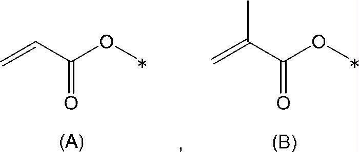
又,丙烯醯胺基為由式(C)表示之官能團,甲基丙烯醯胺基為由式(D)表示之官能團。*表示鍵結位置。Moreover, the acrylamide group is a functional group represented by formula (C), and the methacrylamide group is a functional group represented by formula (D). * Indicates bond position.
[化4]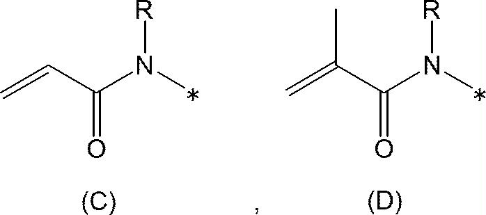
當R為氫原子時,式(C)表示丙-2-烯醯胺基,式(D)表示2-甲基丙-2烯醯胺基。When R is a hydrogen atom, the formula (C) represents a prop-2-acrylamide group, and the formula (D) represents a 2-methylprop-2-acrylamide group.
2官能單體具有聚氧化烯基為較佳。 聚氧化烯基是指,作為重複單元而具有氧化烯基之基團。作為聚氧化烯基,由式(E)表示之基團為較佳。 式(E) -(A-O)m - A表示伸烷基。伸烷基中的碳數並無特別限制,1~4為較佳,2~3為更佳。例如,當A為碳數1的伸烷基時,-(A-O)-表示氧亞甲基(-CH2 O-),當A為碳數2的伸烷基時,-(A-O)-表示氧伸乙基(-CH2 CH2 O-),當A為碳數3的伸烷基時,-(A-O)-表示氧伸丙基(-CH2 CH(CH3 )O-、-CH(CH3 )CH2 O-或-CH2 CH2 CH2 O-)。此外,伸烷基可以是直鏈狀,亦可以是分支鏈狀。The bifunctional monomer preferably has a polyoxyalkylene group. The polyoxyalkylene group means a group having an oxyalkylene group as a repeating unit. As the polyoxyalkylene group, a group represented by the formula (E) is preferred. Formula (E) -(AO) m - A represents an alkylene group. The number of carbons in the alkylene group is not particularly limited, and 1-4 is preferred, and 2-3 is more preferred. For example, when A is an alkylene group with 1 carbon number, -(AO)- means oxymethylene (-CH 2 O-), and when A is an alkylene group with 2 carbon numbers, -(AO)- means Oxygenyl (-CH 2 CH 2 O-), when A is an alkylene group with 3 carbons, -(AO)- means oxypropylidene (-CH 2 CH(CH 3 )O-, -CH (CH 3 )CH 2 O- or -CH 2 CH 2 CH 2 O-). In addition, the alkylene group may be linear or branched.
m表示氧化烯基的重複數,且表示2以上的整數。重複數m被限制成連結鏈的主鏈的原子數成為25個~100個的範圍。 此外,複數個氧化烯基中的伸烷基的碳數可以相同,亦可以不同。例如,式(E)中,含有複數個由-(A-O)-表示之重複單元,各重複單元中的伸烷基中的碳數可以相同,亦可以不同。例如,-(A-O)m -中,可以含有氧亞甲基和氧伸丙基。 又,當含有複數種氧化烯基時,它們的鍵結順序並無特別限制,可以是無規則型,亦可以是嵌段型。m represents the repeating number of the oxyalkylene group, and represents an integer of 2 or more. The repeating number m is limited to a range of 25 to 100 atoms in the main chain linking the chains. In addition, the number of carbon atoms of the alkylene groups in the plurality of oxyalkylene groups may be the same or different. For example, in formula (E), there are multiple repeating units represented by -(AO)-, and the number of carbons in the alkylene group in each repeating unit may be the same or different. For example, -(AO) m - may contain oxymethylene and oxypropylene. Also, when a plurality of oxyalkylene groups are contained, their bonding order is not particularly limited, and may be random or block.
(2官能(甲基)丙烯酸酯單體) 當自由基聚合性基團選自包括丙烯醯氧基及甲基丙烯醯氧基之群組時,作為2官能單體的較佳例,可舉出由式(1)表示之化合物。此外,本說明書中,“(甲基)丙烯酸酯”作為“丙烯酸酯”及“甲基丙烯酸酯”的總稱而使用。(2-functional (meth)acrylate monomer) When the radical polymerizable group is selected from the group including acryloxy group and methacryloxy group, a compound represented by formula (1) is mentioned as a preferable example of the bifunctional monomer. In addition, in this specification, "(meth)acrylate" is used as a generic term of "acrylate" and "methacrylate".
[化5]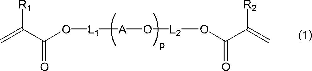
式(1)中,R1 及R2 分別獨立地表示氫原子或甲基,A表示伸烷基,p表示氧伸烷基單元(A-O)的重複數。 A的定義與式(E)中的A的定義相同。 L1 及L2 表示單鍵或2價連接基。上述2價連接基的種類並無特別限制,例如,可舉出2價烴基(可以是2價飽和烴基,亦可以是2價芳香族烴基。2價飽和烴基可以是直鏈狀、分支鏈狀或環狀,碳數1~20為較佳,例如可舉出伸烷基。又,2價芳香族烴基的碳數5~20為較佳,例如可舉出伸苯基。除此以外,亦可以是伸烯基、伸炔基。)、2價雜環基、-O-、-S-、-SO2 -、-NR10 -、-CO-(-C(=O)-)、-COO-(-C(=O)O-)、-NR10 -CO-、-CO-NR10 -、-SO3 -、-SO2 NR10 -及將它們組合兩種以上而成之基團。其中,R10 表示氫原子或烷基(較佳為碳數1~10)。 此外,上述2價連接基中的氫原子可以被鹵素原子等其他取代基取代。In the formula (1), R 1 and R 2 independently represent a hydrogen atom or a methyl group, A represents an alkylene group, and p represents the repeating number of an oxyalkylene unit (AO). The definition of A is the same as the definition of A in formula (E). L 1 and L 2 represent a single bond or a divalent linking group. The type of the above-mentioned 2-valent linking group is not particularly limited, for example, a 2-valent hydrocarbon group (which can be a 2-valent saturated hydrocarbon group, or a 2-valent aromatic hydrocarbon group. The 2-valent saturated hydrocarbon group can be a straight chain or a branched chain) or cyclic, preferably having 1 to 20 carbon atoms, such as an alkylene group. Also, a divalent aromatic hydrocarbon group having 5 to 20 carbon atoms is preferred, such as a phenylene group. In addition, It can also be alkenyl, alkynyl.), divalent heterocyclic group, -O-, -S-, -SO 2 -, -NR 10 -, -CO-(-C(=O)-), -COO-(-C(=O)O-), -NR 10 -CO-, -CO-NR 10 -, -SO 3 -, -SO 2 NR 10 - and combinations of two or more of them group. Wherein, R 10 represents a hydrogen atom or an alkyl group (preferably having 1 to 10 carbon atoms). In addition, the hydrogen atom in the above-mentioned divalent linking group may be substituted with other substituents such as a halogen atom.
上述p係連結2個自由基聚合性基團之“-L1 -(A-O)p -L2 -”的主鏈的原子數成為25個~100個的範圍內之整數。The above-mentioned p is an integer in the range of 25 to 100 atoms in the main chain of "-L 1 -(AO) p -L 2 -" linking two radically polymerizable groups.
作為由式(1)表示之化合物的較佳態樣,可舉出由式(10)表示之化合物。As a preferable aspect of the compound represented by formula (1), the compound represented by formula (10) is mentioned.
[化6]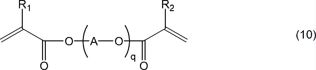
式(10)中,R1 、R2 及A的定義分別與式(1)中的R1 、R2 及A相同,q表示氧伸烷基單元(A-O)的重複數。In formula (10), the definitions of R 1 , R 2 and A are the same as those of R 1 , R 2 and A in formula (1), and q represents the repeating number of oxyalkylene units (AO).
上述q係連結2個自由基聚合性基團之“-(A-O)q-1 -A-”的主鏈的原子數成為25個~100個的範圍內之整數。例如,當A表示乙烯基時,q係3~33的整數,當A表示正丙烯基時,q係6~24的整數。The above-mentioned q is an integer in the range of 25 to 100 atoms in the main chain of "-(AO) q-1 -A-" linking two radically polymerizable groups. For example, when A represents a vinyl group, q is an integer of 3-33, and when A represents a normal propenyl group, q is an integer of 6-24.
作為由上述式(1)表示之化合物,由式(100)表示之化合物為更佳。As the compound represented by the above-mentioned formula (1), a compound represented by the formula (100) is more preferable.
[化7]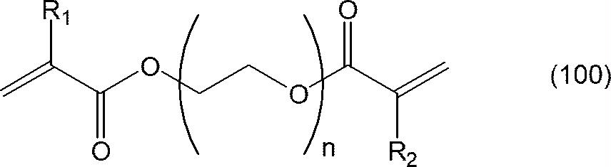
式(100)中,R1 及R2 的定義分別與式(1)中的R1 及R2 相同,n係9~33的整數。In formula (100), the definitions of R 1 and R 2 are the same as those of R 1 and R 2 in formula (1), and n is an integer of 9-33.
作為由式(100)表示之化合物的具體例,可舉出R1 及R2 均係氫原子或甲基,且n=9、14或23者,但並不限定於該等。Specific examples of the compound represented by the formula (100) include those in which both R 1 and R 2 are hydrogen atoms or methyl groups, and n=9, 14, or 23, but are not limited thereto.
(2官能(甲基)丙烯醯胺單體) 當自由基聚合性基團選自包括丙烯醯胺基及甲基丙烯醯胺基之群組時,作為2官能單體的較佳例,可舉出由式(2)表示之化合物。(2-functional (meth)acrylamide monomer) When the radically polymerizable group is selected from the group including an acrylamide group and a methacrylamide group, a compound represented by the formula (2) is mentioned as a preferable example of the bifunctional monomer.
[化8]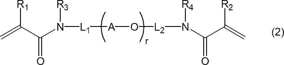
式(2)中,R1 及R2 分別獨立地表示氫原子或甲基,R3 及R4 分別獨立地表示氫原子或取代基,L1 及L2 分別獨立地表示單鍵或2價連接基,A表示伸烷基,r表示氧伸烷基單元(A-O)的重複數。 A的定義與式(E)中A的定義相同。 L1 及L2 的定義與式(1)中的L1 及L2 的定義相同。In formula (2), R 1 and R 2 independently represent a hydrogen atom or a methyl group, R 3 and R 4 independently represent a hydrogen atom or a substituent, and L 1 and L 2 independently represent a single bond or a divalent As a linking group, A represents an alkylene group, and r represents the repeating number of an oxyalkylene group unit (AO). The definition of A is the same as the definition of A in formula (E). The definitions of L 1 and L 2 are the same as the definitions of L 1 and L 2 in the formula (1).
由R3 及R4 表示之取代基的種類並無特別限制,可舉出公知的取代基(例如,可以包含雜原子之脂肪族烴基、芳香族烴基等。更具體而言,為烷基、芳基等。)。The types of substituents represented by R3 and R4 are not particularly limited, and known substituents (for example, aliphatic hydrocarbon groups that may contain heteroatoms, aromatic hydrocarbon groups, etc.. More specifically, alkyl, Aryl, etc.).
上述r為連結2個自由基聚合性基團之“-L1 -(A-O)p -L2 -”的主鏈的原子數成為25個~100個的範圍內之整數。The aforementioned r is an integer within the range of 25 to 100 atoms in the main chain of "-L 1 -(AO) p -L 2 -" connecting two radically polymerizable groups.
作為由式(2)表示之化合物的較佳態樣,可舉出由式(20)表示之化合物。As a preferable aspect of the compound represented by formula (2), the compound represented by formula (20) is mentioned.
[化9]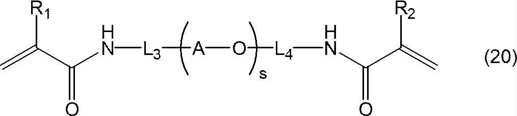
式(20)中,R1 、R2 及A的定義分別與式(2)中的R1 、R2 及A相同,L3 及L4 分別獨立地表示-O-、碳數1~4的伸烷基、由式(F)表示之基團或組合該等而成之2價連接基,s表示氧伸烷基單元(A-O)的重複數。In formula (20), the definitions of R 1 , R 2 and A are the same as those of R 1 , R 2 and A in formula (2), and L 3 and L 4 independently represent -O-, carbon number 1-4 The alkylene group, the group represented by the formula (F) or the divalent linking group formed by combining them, s represents the repeating number of the oxyalkylene unit (AO).
[化10]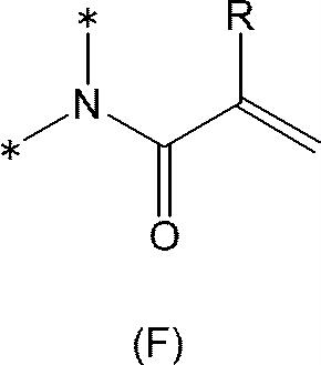
式(F)中,R表示氫原子或甲基,*表示鍵結位置。In formula (F), R represents a hydrogen atom or a methyl group, and * represents a bonding position.
上述s係連結2個自由基聚合性基團之“-L3 -(A-O)s -L4 -”的主鏈的原子數成為25個~100個的範圍內之整數。The above s is an integer in the range of 25 to 100 atoms in the main chain of "-L 3 -(AO) s -L 4 -" linking two radically polymerizable groups.
(2官能單體的含量) 被鍍層前驅物層(或、被鍍層形成用組成物)中的2官能單體的含量並無特別限制,相對於總固體成分,10質量%~90質量%的情況較多,但從進一步抑制被鍍層前驅物層的黏性之方面考慮,相對於總固體成分,係20質量%~80質量%為較佳,從被鍍層的延伸性與電鍍析出性的平衡進一步優異之方面考慮,25質量%~75質量%為更佳。 其中,固體成分是指構成被鍍層之成分,且不包含溶劑。此外,只要為構成被鍍層之成分,則其性狀可以為液體狀,且包含於固體成分中。(content of 2 functional monomers) The content of the bifunctional monomer in the precursor layer of the coating to be coated (or the composition for forming the coating to be coated) is not particularly limited, and it is often 10% to 90% by mass relative to the total solid content, but it is further suppressed In consideration of the viscosity of the coating precursor layer, 20 mass % to 80 mass % is better relative to the total solid content, and in consideration of a further excellent balance between the extensibility of the coating and the electroplating precipitation, 25 mass % % to 75% by mass is more preferable. Here, the solid content refers to the components constituting the layer to be plated, and does not contain a solvent. In addition, as long as it is a component constituting the layer to be plated, its properties may be liquid and contained in the solid component.
《相互作用性聚合物》 相互作用性聚合物係具有與電鍍觸媒或其前驅物相互作用之官能團(以下,有時簡稱為“相互作用性基團”。)之聚合物。"Interactive Polymers" The interactive polymer is a polymer having a functional group (hereinafter, sometimes simply referred to as "interactive group") that interacts with the electroplating catalyst or its precursor.
(相互作用性基團) 相互作用性基團是指,能夠與賦予於被鍍層之電鍍觸媒或其前驅物相互作用之官能團,例如,可舉出能夠與電鍍觸媒或其前驅物形成靜電相互作用之官能團以及能夠與電鍍觸媒或其前驅物形成配位之含氮官能團、含硫官能團及含氧官能團。 作為上述相互作用性基團,例如可舉出胺基、醯胺基、醯亞胺基、脲基、三級胺基、銨基、脒基、三𠯤環、三唑環、苯并三唑基、咪唑基、苯并咪唑基、喹啉基、吡啶基、嘧啶基、吡𠯤基、唑啉基、喹噁啉基、嘌呤基、三𠯤基、哌啶基、哌𠯤基、吡咯啶基、吡唑基、苯胺基、含有烷基胺結構的基、含有異三聚氰酸結構的基、硝基、亞硝基、偶氮基、重氮基、疊氮基、氰基、氰酸酯基等含氮官能團;醚基、羥基、酚性羥基、羧基、碳酸酯基、羰基、酯基、含有N-氧化物結構的基團、含有S-氧化物結構的基、含有N-羥基結構的基團等含氧官能團;噻吩基、硫醇基、硫脲基、硫代三聚氰酸基、苯并噻唑基、巰基三𠯤基、硫醚基、硫酮基、亞碸基、碸基、亞硫酸基、含有磺醯亞胺結構的基、含有亞硫鎓鹽結構的基、磺酸基、含有磺酸酯結構的基等含硫官能團;磷酸酯基、磷醯胺基、膦基、含有磷酸酯結構的基等含磷官能團;含有氯原子及溴原子等鹵素原子的基等,於可採用鹽結構的官能團中,亦能夠使用該等官能團的鹽。 作為上述相互作用性基團,由於極性高,對電鍍觸媒或其前驅物等的吸附能高,因此羧酸基、磺酸基、磷酸基及硼酸基等離子性極性基或氰基為較佳,羧酸基或氰基為更佳。 上述相互作用性聚合物可以具有2種以上的相互作用性基團。(interactive group) The interactive group refers to the functional group that can interact with the electroplating catalyst or its precursor that is given to the plated layer, for example, the functional group that can form electrostatic interaction with the electroplating catalyst or its precursor and the Nitrogen-containing functional groups, sulfur-containing functional groups, and oxygen-containing functional groups that form coordination with electroplating catalysts or their precursors. Examples of the above-mentioned interactive groups include amino groups, amido groups, amido groups, ureido groups, tertiary amino groups, ammonium groups, amidino groups, triazole rings, triazole rings, and benzotriazole groups. Base, imidazolyl, benzimidazolyl, quinolinyl, pyridyl, pyrimidinyl, pyridyl, oxazolinyl, quinoxalinyl, purinyl, trisyl, piperidyl, piperyl, pyrrolidinyl group, pyrazolyl group, aniline group, group containing alkylamine structure, group containing isocyanuric acid structure, nitro group, nitroso group, azo group, diazo group, azido group, cyano group, cyano group Nitrogen-containing functional groups such as ester groups; ether groups, hydroxyl groups, phenolic hydroxyl groups, carboxyl groups, carbonate groups, carbonyl groups, ester groups, groups containing N-oxide structures, groups containing S-oxide structures, groups containing N- Oxygen-containing functional groups such as hydroxyl structure groups; thienyl, thiol, thiourea, thiocyanuric acid, benzothiazolyl, mercaptotrithiol, thioether, thioketone, and arylene groups Sulfur-containing functional groups such as sulfonyl group, sulfite group, group containing sulfonimide structure, group containing sulfinium salt structure, sulfonic acid group, group containing sulfonate structure; phosphate group, phosphoramidide group Phosphorus-containing functional groups such as phosphine groups and groups containing phosphate ester structures; groups containing halogen atoms such as chlorine atoms and bromine atoms, etc. Among the functional groups that can adopt salt structures, salts of these functional groups can also be used. As the above-mentioned interactive groups, due to their high polarity and high adsorption energy to electroplating catalysts or their precursors, carboxylic acid groups, sulfonic acid groups, phosphoric acid groups, boric acid groups and other ionic polar groups or cyano groups are preferred. , a carboxylic acid group or a cyano group is more preferable. The above-mentioned interactive polymer may have two or more types of interactive groups.
上述相互作用性聚合物中含有具有相互作用性基團之重複單元為較佳。 作為具有相互作用性基團之重複單元的一較佳態樣,可舉出由式(G)表示之重複單元。It is preferable that the above-mentioned interactive polymer contains a repeating unit having an interactive group. A repeating unit represented by formula (G) is mentioned as a preferable aspect of the repeating unit which has an interactive group.
[化11]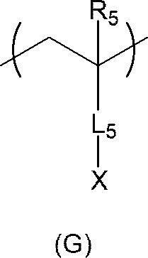
式(G)中,R5 表示氫原子或烷基,L5 表示單鍵或2價連接基,X表示相互作用性基團。In the formula (G), R 5 represents a hydrogen atom or an alkyl group, L 5 represents a single bond or a divalent linking group, and X represents an interactive group.
上述烷基並無特別限定,但碳數係1~5的烷基為較佳,碳數係1~3的烷基為更佳。作為烷基的具體例,可舉出甲基、乙基、2-丙基(異丙基)及丙基(n-正丙基),其中,甲基或乙基為較佳。The above-mentioned alkyl group is not particularly limited, but an alkyl group with 1 to 5 carbon atoms is preferred, and an alkyl group with 1 to 3 carbon atoms is more preferred. Specific examples of the alkyl group include methyl, ethyl, 2-propyl (isopropyl) and propyl (n-n-propyl), among which methyl or ethyl is preferred.
上述2價連接基並無特別限定,例如可舉出2價烴基(可以為2價飽和烴基,亦可以為2價芳香族烴基。2價飽和烴基可以為直鏈狀、支鏈狀或環狀,碳數1~20為較佳,例如可舉出伸烷基。又,2價芳香族烴基的碳數係5~20為較佳,例如可舉出伸芳基。除此以外,可以為伸烯基、伸炔基。)、2價雜環基、-O-、-S-、-SO2 -、-NR10 -、-CO-(-C(=O)-)、-COO-(-C(=O)O-)、-NR10 -CO-、-CO-NR10 -、-SO3 -、-SO2 NR10 -及將該等組合2種以上而成之基團。其中,R10 表示氫原子或烷基(較佳為碳數1~10)。 此外,上述2價連接基中的氫原子可以經鹵素原子等其他取代基取代。The above-mentioned divalent linking group is not particularly limited, for example, a divalent hydrocarbon group (which can be a divalent saturated hydrocarbon group, or a divalent aromatic hydrocarbon group. The divalent saturated hydrocarbon group can be linear, branched or cyclic) , carbon number 1-20 is preferable, for example, an alkylene group can be mentioned. Also, the carbon number of a divalent aromatic hydrocarbon group is preferably 5-20, for example, an arylylene group can be mentioned. In addition, it can be alkenylene, alkynylene.), divalent heterocyclic group, -O-, -S-, -SO 2 -, -NR 10 -, -CO-(-C(=O)-), -COO- (-C(=O)O-), -NR 10 -CO-, -CO-NR 10 -, -SO 3 -, -SO 2 NR 10 -, and a combination of two or more of these. Wherein, R 10 represents a hydrogen atom or an alkyl group (preferably having 1 to 10 carbon atoms). In addition, hydrogen atoms in the above-mentioned divalent linking groups may be substituted with other substituents such as halogen atoms.
上述相互作用性基團如上所述。The above-mentioned interactive groups are as described above.
作為具有相互作用性基團之重複單元的另一較佳態樣,可舉出源自不飽和羧酸或其衍生物之重複單元。 不飽和羧酸是指,具有羧酸基(-COOH基)之不飽和化合物。關於不飽和羧酸的衍生物,例如可舉出不飽和羧酸的酸酐、不飽和羧酸的鹽、不飽和羧酸的單酯等。 作為不飽和羧酸,例如可舉出丙烯酸、甲基丙烯酸、巴豆酸、異巴豆酸、順丁烯二酸、富馬酸、衣康酸及檸康酸等。Another preferred aspect of the repeating unit having an interactive group is a repeating unit derived from an unsaturated carboxylic acid or a derivative thereof. The unsaturated carboxylic acid refers to an unsaturated compound having a carboxylic acid group (-COOH group). Derivatives of unsaturated carboxylic acids include, for example, acid anhydrides of unsaturated carboxylic acids, salts of unsaturated carboxylic acids, monoesters of unsaturated carboxylic acids, and the like. Examples of unsaturated carboxylic acids include acrylic acid, methacrylic acid, crotonic acid, isocrotonic acid, maleic acid, fumaric acid, itaconic acid, and citraconic acid.
上述相互作用性聚合物中的具有相互作用性基團之重複單元的含量並無特別限制,從被鍍層的延伸性及電鍍析出性的平衡的觀點考慮,相對於總重複單元係1~90莫耳%為較佳,30~70莫耳%為更佳。The content of the repeating unit having an interactive group in the above-mentioned interactive polymer is not particularly limited, and is 1 to 90 moles relative to the total repeating unit from the viewpoint of the balance of the extensibility of the layer to be plated and the electroplating deposition property. Mole% is better, and 30-70 mole% is more preferable.
(聚合性官能團) 上述相互作用性聚合物還可以具有聚合性官能團。 聚合性官能團是指,藉由能量賦予可形成化學鍵之官能團,例如可舉出自由基聚合性官能團及陽離子聚合性官能團等。 作為上述聚合性官能團,從反應性更優異之方面考慮,自由基聚合性官能團為較佳。 作為上述自由基聚合性官能團,例如可舉出伸烯基、丙烯酸酯基(丙烯醯氧基)、甲基丙烯酸酯基(甲基丙烯醯氧基)、衣康酸酯基、巴豆酸酯基,異巴豆酸酯基、順丁烯二酸酯基等不飽和羧酸酯基、苯乙烯基、乙烯基、丙烯醯胺基和甲基丙烯醯胺基等。 上述聚合性基團可以包含於相互作用性聚合物的主鏈及側鏈中的任一個中。例如,可以為伸烯基包含於主鏈中之態樣。(polymerizable functional group) The above-mentioned interactive polymer may also have a polymerizable functional group. The polymerizable functional group refers to a functional group capable of forming a chemical bond by energy provision, and examples thereof include a radical polymerizable functional group, a cation polymerizable functional group, and the like. As the above-mentioned polymerizable functional group, a radical polymerizable functional group is preferable from the point of being more excellent in reactivity. Examples of the above-mentioned radically polymerizable functional group include an alkenyl group, an acrylate group (acryloxy group), a methacrylate group (methacryloxy group), an itaconate group, and a crotonate group. , Unsaturated carboxylate groups such as isocrotonate group and maleate group, styryl group, vinyl group, acrylamide group and methacrylamide group, etc. The aforementioned polymerizable group may be included in either the main chain or the side chain of the interactive polymer. For example, an aspect in which an alkenylene group is included in the main chain may be used.
(相互作用性聚合物的較佳態樣) 作為上述相互作用性聚合物的較佳態樣,從以較少的能量賦予量(例如,曝光量)輕鬆地形成被鍍層之方面考慮,可舉出具有源自共軛二烯化合物的重複單元及源自不飽和羧酸或其衍生物的重複單元之聚合物X。 關於源自不飽和羧酸或其衍生物的重複單元的說明如上述。(Best form of interactive polymer) As a preferable aspect of the above-mentioned interactive polymer, from the viewpoint of easily forming a plated layer with a small amount of energy imparted (for example, exposure amount), there are repeating units derived from a conjugated diene compound. and polymer X derived from repeating units of unsaturated carboxylic acids or derivatives thereof. The description of the repeating unit derived from an unsaturated carboxylic acid or a derivative thereof is as above.
作為共軛二烯化合物,若為以1個單鍵隔開之、含有具有2個碳-碳雙鍵之分子結構之化合物,則並無特別限制。 作為共軛二烯化合物,例如可舉出異戊二烯、1,3-丁二烯、1,3-戊二烯、2,4-己二烯、1,3-己二烯、1,3-庚二烯、2,4-庚二烯、1,3-辛二烯、2,4-辛二烯、3,5-辛二烯、1,3-壬二烯、2,4-壬二烯、3,5-壬二烯、1,3-癸二烯、2,4-癸二烯、3,5-癸二烯、2,3-二甲基-丁二烯、2-甲基-1,3-戊二烯、3-甲基-1,3-戊二烯、4-甲基-1,3-戊二烯、2-苯基-1,3-丁二烯、2-苯基-1,3-戊二烯、3-苯基-1,3-戊二烯、2,3-二甲基-1,3-戊二烯、4-甲基-1,3-戊二烯、2-己基-1,3-丁二烯、3-甲基-1,3-己二烯、2-苄基-1,3-丁二烯及2-對甲苯基-1,3-丁二烯等。The conjugated diene compound is not particularly limited as long as it is a compound having a molecular structure having two carbon-carbon double bonds separated by one single bond. Examples of conjugated diene compounds include isoprene, 1,3-butadiene, 1,3-pentadiene, 2,4-hexadiene, 1,3-hexadiene, 1, 3-heptadiene, 2,4-heptadiene, 1,3-octadiene, 2,4-octadiene, 3,5-octadiene, 1,3-nonadiene, 2,4- Nonadiene, 3,5-Nadiene, 1,3-Decadiene, 2,4-Decadiene, 3,5-Decadiene, 2,3-Dimethyl-butadiene, 2- Methyl-1,3-pentadiene, 3-methyl-1,3-pentadiene, 4-methyl-1,3-pentadiene, 2-phenyl-1,3-butadiene, 2-Phenyl-1,3-pentadiene, 3-phenyl-1,3-pentadiene, 2,3-dimethyl-1,3-pentadiene, 4-methyl-1,3 -pentadiene, 2-hexyl-1,3-butadiene, 3-methyl-1,3-hexadiene, 2-benzyl-1,3-butadiene and 2-p-tolyl-1 , 3-butadiene, etc.
其中,從容易合成聚合物X,且被鍍層的特性更加優異之方面考慮,源自共軛二烯化合物的重複單元係源自具有由式(3)表示之丁二烯骨架之化合物的重複單元為較佳。Among them, the repeating unit derived from a conjugated diene compound is a repeating unit derived from a compound having a butadiene skeleton represented by the formula (3) in view of the ease of synthesizing the polymer X and the better properties of the coated layer. is better.
[化12]
式(3)中,R6 分別獨立地表示氫原子、鹵素原子或烴基。作為烴基,可舉出脂肪族烴基(例如,烷基、烯基等。碳數1~12為較佳。)及芳香族烴基(例如,苯基、萘基等。)。具有複數個之R6 可以彼此相同,亦可以不同。In formula (3), R 6 each independently represent a hydrogen atom, a halogen atom or a hydrocarbon group. Examples of the hydrocarbon group include aliphatic hydrocarbon groups (eg, alkyl, alkenyl, etc., preferably having 1 to 12 carbon atoms.) and aromatic hydrocarbon groups (eg, phenyl, naphthyl, etc.). The plural R 6 may be the same as or different from each other.
作為具有由式(3)表示之丁二烯骨架之化合物(具有丁二烯結構之單體),例如可舉出1,3-丁二烯、異戊二烯、2-乙基-1,3-丁二烯、2-正丙基-1,3-丁二烯、2,3-二甲基-1,3-丁二烯、1-苯基-1,3-丁二烯、1-α-萘基-1,3-丁二烯、1-β-萘基-1,3-丁二烯、2-氯-1,3-丁二烯、1-溴-1,3-丁二烯、1-氯丁二烯、2-氟-1,3-丁二烯、2,3-二氯-1,3-丁二烯及1,1,2-三氯-1,3-丁二烯、2-氰基-1,3-丁二烯等。Examples of compounds having a butadiene skeleton represented by formula (3) (monomers having a butadiene structure) include 1,3-butadiene, isoprene, 2-ethyl-1, 3-butadiene, 2-n-propyl-1,3-butadiene, 2,3-dimethyl-1,3-butadiene, 1-phenyl-1,3-butadiene, 1 -α-naphthyl-1,3-butadiene, 1-β-naphthyl-1,3-butadiene, 2-chloro-1,3-butadiene, 1-bromo-1,3-butadiene Diene, 1-chlorobutadiene, 2-fluoro-1,3-butadiene, 2,3-dichloro-1,3-butadiene and 1,1,2-trichloro-1,3- Butadiene, 2-cyano-1,3-butadiene, etc.
相對於總重複單元,聚合物X中的源自共軛二烯化合物的重複單元的含量係25~75莫耳%為較佳。 相對於總重複單元,聚合物X中的源自不飽和羧酸或其衍生物的重複單元的含量係25~75莫耳%為較佳。The content of the repeating unit derived from the conjugated diene compound in the polymer X is preferably 25 to 75 mol % with respect to the total repeating units. The content of repeating units derived from unsaturated carboxylic acids or derivatives thereof in polymer X is preferably 25 to 75 mol% relative to the total repeating units.
(相互作用性聚合物的重量平均分子量) 上述相互作用性聚合物的重量平均分子量並無特別限制,從操作性進一步優異之方面考慮,10000~700000為較佳,20000~500000為更佳。(weight average molecular weight of the interacting polymer) The weight average molecular weight of the above-mentioned interactive polymer is not particularly limited, but is preferably from 10,000 to 700,000, and more preferably from 20,000 to 500,000, from the viewpoint of further improving handleability.
(相互作用性聚合物的具體例) 作為上述相互作用性聚合物的具體例,可舉出1,3-丁二烯與順丁烯二酸酐的交替共聚物亦即丁二烯-順丁烯二酸共聚物、聚丙烯酸及聚甲基丙烯酸,但並不限定於該等。(Specific examples of interactive polymers) Specific examples of the above-mentioned interactive polymers include butadiene-maleic acid copolymers, polyacrylic acid, and polymethylmethacrylate, which are alternating copolymers of 1,3-butadiene and maleic anhydride. Acrylic acid, but not limited to these.
(相互作用性聚合物的含量) 被鍍層前驅物層(或被鍍層形成用組成物)中的上述相互作用性聚合物的含量並無特別限制,相對於總固體成分為10質量%~90質量%的情況較多,但從進一步抑制被鍍層前驅物層的黏性之方面考慮,相對於總固體成分係20質量%~80質量%為較佳,從被鍍層的延伸性與電鍍析出性的平衡優異之方面考慮,25質量%~75質量%為更佳。 其中,固體成分是指構成被鍍層之成分,且不包含溶劑。此外,只要為構成被鍍層之成分,則其性狀可以為液體狀,且包含於固體成分中。(content of interactive polymer) The content of the above-mentioned interactive polymer in the to-be-plated precursor layer (or the composition for forming the to-be-plated layer) is not particularly limited, and it is often 10 mass % to 90 mass % with respect to the total solid content, but from further From the aspect of suppressing the viscosity of the coating precursor layer, 20 mass % to 80 mass % is better relative to the total solid content, and from the aspect of excellent balance between the extensibility of the coating and plating precipitation, 25 mass % ~75% by mass is more preferable. Here, the solid content refers to the components constituting the layer to be plated, and does not contain a solvent. In addition, as long as it is a component constituting the layer to be plated, its properties may be liquid and contained in the solid component.
上述相互作用性聚合物的質量與上述2單官能單體的質量之比(相互作用性聚合物的質量/2單官能單體的質量)並無特別限制,0.1~10的情況較多,從被鍍層前驅物層的觸控性被進一步抑制之方面考慮,0.3~3.0為較佳,0.5~1.5為更佳。The ratio of the mass of the above-mentioned interactive polymer to the mass of the above-mentioned 2 monofunctional monomers (mass of the interactive polymer/mass of 2 monofunctional monomers) is not particularly limited, and it is often 0.1 to 10, ranging from Considering that the touchability of the precursor layer to be plated is further suppressed, 0.3 to 3.0 is preferable, and 0.5 to 1.5 is more preferable.
《聚合起始劑》 本發明中,被鍍層前驅物層(或被鍍層形成用組成物)可以包含於聚合起始劑。藉由包含聚合起始劑,曝光處理時的聚合性官能團之間的反應更有效地進行。 作為聚合起始劑並無特別限制,能夠使用公知的聚合起始劑(所謂的光聚合起始劑)等。作為聚合起始劑的例,能夠舉出二苯甲酮類、苯乙酮類、α-胺基烷基苯酮類、安息香類、酮類、硫雜蒽酮類、苄基類、苄基縮酮類、肟酯類、蒽酮類、四甲基秋蘭姆單硫化物類、雙醯基氧化膦類、醯基氧化膦類、蒽醌類、偶氮化合物等及其衍生物。 被鍍層形成用組成物中的聚合起始劑的含量並無特別限制,從被鍍層的硬化性的方面考慮,相對於2官能單體及相互作用性聚合物的合計100質量%,係0.1質量%~20質量%為較佳,1質量%~10質量%為更佳。"Polymerization Initiator" In the present invention, the precursor layer of the layer to be plated (or the composition for forming the layer to be plated) may be contained in the polymerization initiator. By including a polymerization initiator, the reaction between the polymerizable functional groups at the time of exposure treatment proceeds more efficiently. The polymerization initiator is not particularly limited, and known polymerization initiators (so-called photopolymerization initiators) and the like can be used. Examples of polymerization initiators include benzophenones, acetophenones, α-aminoalkylphenones, benzoins, ketones, thioxanthones, benzyls, benzyl Ketals, oxime esters, anthrone, tetramethylthiuram monosulfide, bisacyl phosphine oxides, acyl phosphine oxides, anthraquinones, azo compounds, etc. and their derivatives. The content of the polymerization initiator in the composition for forming the layer to be plated is not particularly limited, and it is 0.1% by mass relative to 100% by mass of the total of the bifunctional monomer and the interactive polymer in view of the curability of the layer to be plated. % to 20 mass % is preferable, and 1 mass % to 10 mass % is more preferable.
《溶劑》 從操作性的方面考慮,被鍍層形成用組成物中包含溶劑為較佳。 能夠使用的溶劑並無特別限定,例如可舉出水;甲醇、乙醇、丙醇、乙二醇、1-甲氧基-2-丙醇、甘油、丙二醇單甲醚等醇系溶劑;乙酸等酸;丙酮、甲乙酮、環己酮等酮系溶劑;甲醯胺、二甲基乙醯胺、N-甲基吡咯啶酮等醯胺系溶劑;乙腈、丙腈等腈系溶劑;乙酸甲酯、乙酸乙酯等酯系溶劑;碳酸二甲酯、碳酸二乙酯等碳酸酯系溶劑;除此以外,可舉出醚系溶劑、乙二醇系溶劑、胺系溶劑、硫醇系溶劑及鹵素系溶劑等。 其中,醇系溶劑、醯胺系溶劑、酮系溶劑、腈系溶劑或碳酸酯系溶劑為較佳。 被鍍層形成用組成物中的溶劑的含量並無特別限制,相對於組成物總量,50質量%~98質量%為較佳,70質量%~98質量%為更佳。若在上述範圍內,則組成物的操作性優異,且容易控制圖案狀被鍍層的層厚。"Solvent" From the viewpoint of workability, it is preferable that the composition for forming a layer to be plated contains a solvent. Usable solvents are not particularly limited, and examples include water; alcohol-based solvents such as methanol, ethanol, propanol, ethylene glycol, 1-methoxy-2-propanol, glycerin, and propylene glycol monomethyl ether; acetic acid, etc. Acid; Acetone, methyl ethyl ketone, cyclohexanone and other ketone solvents; Formamide, dimethylacetamide, N-methylpyrrolidone and other amide solvents; Acetonitrile, propionitrile and other nitrile solvents; Methyl acetate , ethyl acetate and other ester-based solvents; dimethyl carbonate, diethyl carbonate and other carbonate-based solvents; in addition, ether-based solvents, glycol-based solvents, amine-based solvents, mercaptan-based solvents, and Halogen solvents, etc. Among them, alcohol-based solvents, amide-based solvents, ketone-based solvents, nitrile-based solvents or carbonate-based solvents are preferred. The content of the solvent in the composition for forming the layer to be plated is not particularly limited, but is preferably 50% by mass to 98% by mass, more preferably 70% by mass to 98% by mass, based on the total amount of the composition. Within the above range, the composition has excellent handleability, and it is easy to control the layer thickness of the patterned layer to be plated.
《其他添加劑》 被鍍層形成用組成物中可以依需要添加其他添加劑(例如,增感劑、硬化劑、聚合抑制劑、抗氧化劑、抗靜電劑、紫外線吸收劑、填料、粒子、阻燃劑、界面活性劑、潤滑劑及增塑劑等)。"Other Additives" Other additives (such as sensitizers, hardeners, polymerization inhibitors, antioxidants, antistatic agents, ultraviolet absorbers, fillers, particles, flame retardants, surfactants, lubricants and plasticizers, etc.).
《被鍍層形成用組成物的製造方法》 被鍍層形成用組成物的製造方法並無特別限制,可舉出公知的方法。例如,可舉出將上述各成分一併混合之方法或將各成分分階段混合之方法等。"Method for producing a composition for forming a layer to be plated" The method for producing the composition for forming a layer to be plated is not particularly limited, and known methods can be used. For example, a method of collectively mixing the above-mentioned components or a method of mixing the components in stages may be mentioned.
<前驅物薄膜的製造方法> 能夠使用上述之被鍍層形成用組成物於基板上形成被鍍層前驅物層。此外,被鍍層前驅物層係藉由實施硬化處理而成為被鍍層之前驅物層,且為實施硬化處理之前的未硬化的狀態的層。<Precursor film manufacturing method> The above-mentioned composition for forming a layer to be plated can be used to form a layer to be plated precursor layer on a substrate. In addition, the precursor layer of the to-be-plated layer becomes the precursor layer of the to-be-plated layer by performing hardening process, and is a layer of the uncured state before hardening process.
作為被鍍層前驅物層的製造方法,具有以下製程之方法為較佳。 製程1:使基板與底漆層形成用組成物接觸而於基板上形成底漆層,接著使形成在基板上之底漆層與被鍍層形成用組成物接觸而於基板上形成底漆層和被鍍層前驅物層之製程As a method of manufacturing the precursor layer of the plated layer, the method with the following process is preferred. Process 1: The substrate is brought into contact with the composition for forming a primer layer to form a primer layer on the substrate, and then the primer layer formed on the substrate is brought into contact with the composition for forming a plated layer to form a primer layer and a composition for forming a plated layer on the substrate. The process of the precursor layer to be plated
製程1為如下製程,亦即使基板與底漆層形成用組成物接觸而於基板上形成底漆層,進而使形成在基板上之底漆層與被鍍層形成用組成物接觸而於基板上形成底漆層和被鍍層前驅物層。藉由實施本製程,可得到具有基板、配置在基板上之底漆層及配置在底漆層上之被鍍層前驅物層之附被鍍層前驅物層基板。Process 1 is a process in which the primer layer is formed on the substrate by contacting the substrate with the composition for forming the primer layer, and then the primer layer formed on the substrate is formed on the substrate by contacting the composition for forming the layer to be plated. Primer layer and coating precursor layer. By implementing this process, a substrate with a substrate to be coated with a precursor layer having a substrate, a primer layer disposed on the substrate, and a precursor layer to be coated disposed on the primer layer can be obtained.
使基板與底漆層形成用組成物接觸之方法並無特別限制,可舉出將底漆層形成用組成物塗佈於基板上之方法或將基板浸漬於底漆層形成用組成物中之方法。 又,使形成在基板上之底漆層與被鍍層形成用組成物層接觸之方法並無特別限制,可舉出於形成有底漆層之基板的底漆層上塗佈電鍍層形成用組成物之方法或將形成有底漆層之基板浸漬於底漆中之方法。 此外,使基板與底漆接觸之後,依需要,可以為了從底漆層去除溶劑而實施乾燥處理。又,使形成在基板上之底漆層與被鍍層形成用組成物接觸之後,依需要,可以為了從被鍍層前驅物層去除溶劑而實施乾燥處理。The method of bringing the substrate into contact with the primer layer-forming composition is not particularly limited, and examples include a method of coating the substrate with the primer layer-forming composition or immersing the substrate in the primer layer-forming composition. method. Also, the method of making the primer layer formed on the substrate contact the layer of the composition for forming the layer to be plated is not particularly limited, and may include coating the composition for forming the plating layer on the primer layer of the substrate on which the primer layer is formed. or a method of immersing the substrate on which the primer layer is formed in the primer. In addition, after the substrate is brought into contact with the primer, a drying treatment may be performed to remove the solvent from the primer layer, if necessary. Furthermore, after the primer layer formed on the substrate is brought into contact with the composition for forming a layer to be plated, a drying treatment may be performed to remove the solvent from the layer to be plated precursor layer if necessary.
[附被鍍層基板] 本發明的附被鍍層基板具有使本發明的前驅物薄膜中的被鍍層前驅物層硬化而成之被鍍層。[with coated substrate] The plated substrate of the present invention has a plated layer obtained by hardening the plated layer precursor layer in the precursor thin film of the present invention.
能夠使用上述之本發明的前驅物薄膜製造附被鍍層基板。此外,被鍍層係實施後述之電鍍處理之層,藉由電鍍處理於其表面上形成金屬層。 作為附被鍍層基板的製造方法,具有以下製程之方法為較佳。A substrate to be plated can be produced using the precursor thin film of the present invention described above. In addition, the layer to be plated is a layer subjected to the electroplating treatment described later, and a metal layer is formed on the surface by the electroplating treatment. As a method of manufacturing a plated substrate, a method having the following processes is preferable.
製程2:對前驅物薄膜中的被鍍層前驅物層實施硬化處理而形成被鍍層之製程Process 2: The process of hardening the coating precursor layer in the precursor thin film to form the coating
製程2為對被鍍層前驅物層實施硬化處理而形成被鍍層之製程。 硬化處理的方法並無特別限制,可舉出加熱處理及曝光處理(光照射處理)。其中,從短時間內結束處理之方面考慮,曝光處理為較佳。藉由硬化處理,被鍍層前驅物層中的化合物中所含有之聚合性基團被活性化,且與化合物之間產生交聯,從而進行層的硬化。 此外,實施上述硬化處理(尤其,曝光處理)時,可以以得到所希望的圖案狀實施硬化處理,以便得到所希望的圖案狀被鍍層。例如,使用具有規定形狀的開口部之遮罩進行曝光處理為較佳。此外,對以圖案狀實施了硬化處理之被鍍層前驅物層實施顯影處理,藉此形成圖案狀被鍍層。 顯影處理的方法並無特別限制,依所使用的材料的種類實施最佳的顯影處理。作為顯影液,例如可舉出有機溶劑、純水及鹼水溶液,較佳為鹼水溶液。作為鹼水溶液的例,可舉出碳酸鈉水溶液、碳酸氫鈉水溶液、碳酸鉀水溶液及碳酸氫鉀水溶液等,但並不限定於該等。Process 2 is a process of hardening the precursor layer of the layer to be plated to form the layer to be plated. The method of hardening treatment is not particularly limited, and examples thereof include heat treatment and exposure treatment (light irradiation treatment). Among them, exposure processing is preferable from the viewpoint of completing the processing in a short time. By the hardening treatment, the polymerizable group contained in the compound in the precursor layer to be plated is activated, and cross-linking occurs with the compound, thereby hardening the layer. In addition, when the above-mentioned hardening treatment (in particular, exposure treatment) is performed, the hardening treatment may be performed so that a desired pattern shape is obtained so that a desired pattern shape to-be-plated layer is obtained. For example, it is preferable to perform exposure processing using a mask having an opening of a predetermined shape. In addition, the patterned layer to be plated is formed by developing the precursor layer of the layer to be plated that has been hardened in a pattern. The method of development treatment is not particularly limited, and the optimum development treatment is performed according to the type of material used. As a developing solution, an organic solvent, pure water, and an aqueous alkali solution are mentioned, for example, Preferably it is an aqueous alkali solution. Examples of aqueous alkali solution include, but are not limited to, sodium carbonate aqueous solution, sodium hydrogencarbonate aqueous solution, potassium carbonate aqueous solution, and potassium hydrogencarbonate aqueous solution.
藉由上述方法,使被鍍層形成用組成物硬化而得到之被鍍層配置於基板上。亦即,可得到具有基板和配置在基板上之被鍍層之附被鍍層基板。By the method described above, the layer to be plated obtained by curing the composition for forming a layer to be plated is arranged on the substrate. That is, a plated substrate having a substrate and a layer to be plated on the substrate can be obtained.
被鍍層的平均厚度並無特別限制,0.05~100 μm為較佳,0.07~10 μm為更佳,0.1~3 μm為進一步較佳。 上述平均厚度為利用電子顯微鏡(例如,掃描型電子顯微鏡)對被鍍層的垂直截面進行觀察,測定任意10處的厚度並對該等進行算術平均而得到之平均值。The average thickness of the layer to be plated is not particularly limited, but is preferably 0.05-100 μm, more preferably 0.07-10 μm, and still more preferably 0.1-3 μm. The above-mentioned average thickness is an average value obtained by observing a vertical cross-section of the plated layer with an electron microscope (for example, a scanning electron microscope), measuring the thickness at any 10 places, and arithmetically averaging these.
被鍍層可以形成為圖案狀。例如,被鍍層可以形成為網格狀。圖1中,於基板10上配置有網格狀被鍍層12。
構成被鍍層12的網格之細線部的線寬W的大小並無特別限制,從形成於被鍍層上之金屬層的導電特性及難見性的平衡的方面考慮,30 μm以下為較佳,15 μm以下為更佳,10 μm以下為進一步較佳,5 μm以下為特佳,0.5 μm以上為較佳,1.0 μm以上為更佳。The layer to be plated may be patterned. For example, the layer to be plated may be formed in a grid shape. In FIG. 1 , a grid-shaped layer to be plated 12 is arranged on a
圖1中,開口部14具有大致菱形形狀,但並不限定於該形狀,亦可以是其他的多邊形狀(例如,三角形、四邊形、六邊形、無規則多邊形)。又,可以將一邊的形狀設為直線狀,且其餘設為彎曲狀,亦可以設為圓弧狀。設為圓弧狀時,例如關於相對向的兩邊,可以設為向外側凸出的圓弧狀,且關於其他相對向的兩邊,可以設為向內側凸出的圓弧狀。又,可以將各邊的形狀設為向外側凸出的圓弧與向內側凸出的圓弧連續之波浪線狀。當然,亦可以將各邊的形狀設為正弦曲線。In FIG. 1 , the
開口部14的一邊的長度L並無特別限制,1500 μm以下為較佳,1300 μm以下為更佳,1000 μm以下為進一步較佳,5 μm以上為較佳,30 μm以上為更佳,80 μm以上為進一步較佳。當開口部的一邊的長度為上述範圍時,後述的導電性薄膜的透明性更加優異。The length L of one side of the
此外,可以使上述附被鍍層基板變形而將其設為具有三維形狀之附被鍍層基板。亦即,藉由使上述附被鍍層基板變形,可得到具有具備三維形狀之基板和配置在該基板上之被鍍層(或圖案狀被鍍層)之附被鍍層基板(具有三維形狀之附被鍍層基板)。 如上所述,使上述被鍍層形成用組成物硬化而得到之被鍍層的延伸性優異,且隨著基板的變形能夠使其形狀發生變化。 附被鍍層基板的變形方法並無特別限制,例如,可舉出真空成形、吹塑成形、自由吹塑成形、壓力成形、真空-壓力成形及熱沖壓成形等公知的方法。 例如,如圖2所示,可以將附被鍍層基板的一部分變形為半球狀而設為具有半球狀形狀之附被鍍層基板20。此外,圖2中,未圖示被鍍層。 此外,上述中對賦予三維形狀之態樣進行了說明,但亦可以對附被鍍層基板實施如單軸延伸或雙軸延伸那樣的延伸處理而使其形狀變形。 使附被鍍層基板成形時的加熱溫度並無特別限定,60℃~120℃的範圍內的溫度為較佳,80℃~120℃的範圍內的溫度為更佳。In addition, the above-mentioned substrate to be plated can be transformed into a substrate to be plated having a three-dimensional shape. That is, by deforming the above-mentioned substrate to be coated, a substrate to be coated having a substrate having a three-dimensional shape and a layer to be plated (or a pattern-like layer to be plated) disposed on the substrate can be obtained (the substrate to be plated having a three-dimensional shape substrate). As described above, the to-be-plated layer obtained by curing the above-mentioned composition for forming the to-be-plated layer has excellent extensibility, and can change its shape along with deformation of the substrate. The method of deforming the plated substrate is not particularly limited, and examples thereof include known methods such as vacuum forming, blow molding, free blow molding, pressure forming, vacuum-pressure forming, and hot stamping. For example, as shown in FIG. 2 , a part of the substrate to be plated may be deformed into a hemispherical shape to form a substrate to be plated 20 having a hemispherical shape. In addition, in FIG. 2, the layer to be plated is not shown in figure. In addition, although the mode of imparting a three-dimensional shape has been described above, it is also possible to deform the shape by performing a stretching process such as uniaxial stretching or biaxial stretching on the plated substrate. The heating temperature for forming the plated substrate is not particularly limited, but the temperature in the range of 60°C to 120°C is preferable, and the temperature in the range of 80°C to 120°C is more preferable.
此外,上述中對使附被鍍層基板變形之態樣進行了說明,但並不限定於該態樣,亦可以於使上述附被鍍層前驅物層的基板變形之後,實施上述製程2來得到具有三維形狀之附被鍍層基板。 又,上述中對以圖案狀對被鍍層前驅物層實施硬化處理而形成圖案狀被鍍層之態樣進行了說明,但並不限定於該態樣,將被鍍層前驅物層以圖案狀配置於基板上,並對該圖案狀被鍍層前驅物層實施硬化處理,藉此亦能夠形成圖案狀被鍍層。此外,作為將被鍍層前驅物層以圖案狀配置之方法,例如可舉出藉由網版印刷法或噴墨法向基板上的規定位置賦予被鍍層形成用組成物之方法。In addition, in the above, the aspect of deforming the substrate to be coated has been described, but it is not limited to this aspect. After deforming the substrate with the precursor layer to be coated, the above process 2 can be implemented to obtain a Three-dimensional shape coated substrate. Also, the mode in which the patterned layer to be plated is hardened to form the patterned layer to be plated has been described above, but it is not limited to this mode. The patterned layer to be plated can also be formed by hardening the precursor layer of the patterned layer to be plated on the substrate. Moreover, as a method of arranging the layer-to-be-plated precursor layer in a pattern form, the method of providing the composition for layer-to-be-plated formation to the predetermined position on a board|substrate by screen printing method or an inkjet method is mentioned, for example.
[導電性薄膜、觸控面板感測器及觸控面板] 本發明的導電性薄膜包括本發明的附被鍍層基板及被配置在被鍍層基板中的被鍍層上之金屬層。又,本發明的觸控面板感測器包括本發明的導電性薄膜,且本發明的觸控面板包括本發明的觸控面板感測器。[Conductive film, touch panel sensor and touch panel] The conductive thin film of the present invention includes the substrate to be plated and the metal layer arranged on the layer to be plated in the substrate to be plated according to the present invention. Moreover, the touch panel sensor of the present invention includes the conductive film of the present invention, and the touch panel of the present invention includes the touch panel sensor of the present invention.
對上述附被鍍層基板中的被鍍層實施電鍍處理,藉此能夠於被鍍層上形成金屬層。尤其,當被鍍層以圖案狀配置於基板上時,形成沿該圖案的金屬層(圖案狀金屬層)。 形成金屬層之方法並無特別限制,例如實施對被鍍層賦予電鍍觸媒或其前驅物之製程3及對被賦予了電鍍觸媒或其前驅物之被鍍層實施電鍍處理之製程4為較佳。 以下,對製程3及製程4的步驟進行詳細說明。The metal layer can be formed on the layer to be plated by subjecting the layer to be plated in the substrate with the layer to be plated to electroplating. In particular, when the layer to be plated is arranged in a pattern on the substrate, a metal layer (patterned metal layer) along the pattern is formed. The method of forming the metal layer is not particularly limited. For example, it is better to implement the process 3 of giving the electroplating catalyst or its precursor to the plated layer and the process 4 of implementing electroplating treatment to the plated layer given the electroplating catalyst or its precursor. . Hereinafter, the steps of process 3 and process 4 will be described in detail.
製程3為對被鍍層賦予電鍍觸媒或其前驅物之製程。被鍍層中含有上述相互作用性基團,因此相互作用性基團依其功能而與被賦予的電鍍觸媒或其前驅物黏附(吸附)。 電鍍觸媒或其前驅物作為電鍍處理的觸媒或電極而發揮功能。因此,所使用的電鍍觸媒或其前驅物的種類可藉由電鍍處理的種類而適當確定。Process 3 is the process of imparting an electroplating catalyst or its precursor to the plated layer. The layer to be plated contains the above-mentioned interactive group, so the interactive group adheres (adsorbs) to the given electroplating catalyst or its precursor according to its function. The electroplating catalyst or its precursor functions as a catalyst or electrode for electroplating. Therefore, the type of the electroplating catalyst or its precursor to be used can be appropriately determined by the type of electroplating treatment.
電鍍觸媒或其前驅物係非電解電鍍觸媒或其前驅物為較佳。 關於非電解電鍍觸媒,若是成為非電解電鍍時的活性核者,則並無特別限制,例如,可舉出具有自觸媒還原反應的觸媒能之金屬(作為能夠進行離子化傾向比Ni低的非電解電鍍之金屬而公知者)。具體而言,可舉出Pd、Ag、Cu、Pt、Au及Co等。 作為該非電解電鍍觸媒,可以使用金屬膠體。 關於非電解電鍍觸媒前驅物,若為藉由化學反應而成為非電解電鍍觸媒者,則並無特別限制,例如可舉出作為上述非電解電鍍觸媒而舉出之金屬的離子。The electroplating catalyst or its precursor is preferably an electroless electroplating catalyst or its precursor. With regard to the electroless plating catalyst, if it becomes the active nucleus during electroless plating, then there is no particular limitation, for example, a metal having a catalytic ability of self-catalytic reduction reaction (as a metal capable of ionization tendency than Ni Low electroless plated metals are known). Specifically, Pd, Ag, Cu, Pt, Au, Co, etc. are mentioned. Metal colloid can be used as the electroless plating catalyst. The electroless plating catalyst precursor is not particularly limited as long as it becomes an electroless plating catalyst through a chemical reaction, and examples thereof include ions of the metals mentioned above as the electroless plating catalyst.
作為對被鍍層賦予電鍍觸媒或其前驅物之方法,例如可舉出將電鍍觸媒或其前驅物分散或溶解於溶劑而製備溶液,並將該溶液塗佈於被鍍層上之方法或將附被鍍層基板浸漬於該溶液中之方法。 作為上述溶劑,例如可舉出水或有機溶劑。As a method of imparting a plating catalyst or its precursor to the layer to be plated, for example, a method of preparing a solution by dispersing or dissolving the plating catalyst or its precursor in a solvent, and applying the solution on the layer to be plated or applying A method of immersing the coated substrate in the solution. As said solvent, water or an organic solvent is mentioned, for example.
製程4為對被賦予了電鍍觸媒或其前驅物之被鍍層實施電鍍處理之製程。 電鍍處理的方法並無特別限制,例如可舉出非電解電鍍處理或電解電鍍處理(電鍍處理)。該製程中,可以單獨實施非電解電鍍處理,亦可以於實施了非電解電鍍處理之後進而實施電解電鍍處理。 以下,對非電解電鍍處理及電解電鍍處理的步驟進行詳細說明。Process 4 is a process of performing electroplating treatment on the layer to be plated to which the electroplating catalyst or its precursor has been given. The method of plating treatment is not particularly limited, and examples thereof include electroless plating treatment and electrolytic plating treatment (plating treatment). In this manufacturing process, the electroless plating treatment may be performed alone, or the electrolytic plating treatment may be further performed after the electroless plating treatment is performed. Hereinafter, the steps of the electroless plating treatment and the electrolytic plating treatment will be described in detail.
非電解電鍍處理是指,使用將作為電鍍而欲析出之金屬離子熔化而成之溶液,並藉由化學反應而析出金屬之處理。 作為非電解電鍍處理的步驟,例如對被賦予了非電解電鍍觸媒之附被鍍層基板進行水洗而去除多餘的非電解電鍍觸媒之後,浸漬於非電解電鍍浴為較佳。作為所使用的非電解電鍍浴,能夠使用公知的非電解電鍍浴。 此外,除了溶劑(例如,水)以外,於通常的非電解電鍍浴中主要含有電鍍用金屬離子、還原劑及用於提高金屬離子的穩定性之添加劑(穩定劑)。The electroless plating process refers to a process of depositing a metal by a chemical reaction using a solution obtained by melting metal ions to be deposited as electroplating. As a step of the electroless plating treatment, for example, immersing the substrate to be plated to which the electroless plating catalyst has been given is washed with water to remove excess electroless plating catalyst, and then immersed in an electroless plating bath. As the electroless plating bath to be used, known electroless plating baths can be used. In addition, in addition to a solvent (for example, water), a general electroless plating bath mainly contains metal ions for electroplating, a reducing agent, and additives (stabilizers) for improving the stability of metal ions.
當被賦予到被鍍層之電鍍觸媒或其前驅物具有作為電極的功能時,能夠對被賦予了該觸媒或其前驅物之被鍍層實施電解電鍍處理。 此外,如上所述,於上述非電解電鍍處理之後,能夠依需要而進行電解電鍍處理。該種形態中,能夠適當調整所形成之金屬層的厚度。When the plating catalyst or its precursor given to the layer to be plated has a function as an electrode, electrolytic plating can be performed on the layer to be plated to which the catalyst or its precursor is given. In addition, as described above, after the above-mentioned electroless plating treatment, electrolytic plating treatment can be performed as necessary. In this form, the thickness of the formed metal layer can be adjusted appropriately.
此外,上述中對實施製程3之形態進行了說明,但當被鍍層含有電鍍觸媒或其前驅物時,可以不實施製程3。In addition, the form of implementing process 3 has been described above, but when the layer to be plated contains an electroplating catalyst or its precursor, process 3 may not be implemented.
藉由實施上述處理,可於被鍍層上形成金屬層。亦即,可得到包括附被鍍層基板和配置在附被鍍層基板中的被鍍層上之金屬層之導電性薄膜。 此外,對應於欲形成之圖案狀金屬層的形狀,將圖案狀被鍍層配置於基板上,藉此能夠得到具有所希望的形狀的圖案狀金屬層之導電性薄膜。例如,欲得到網格狀金屬層時,形成網格狀被鍍層即可。 又,使用具有三維形狀之附被鍍層基板,並實施了上述製程3及4時,可得到具有三維形狀之導電性薄膜。By performing the above-mentioned treatment, a metal layer can be formed on the layer to be plated. That is, a conductive thin film including a substrate to be plated and a metal layer disposed on the layer to be plated in the substrate to be plated can be obtained. In addition, a patterned layer to be plated is arranged on the substrate corresponding to the shape of the patterned metal layer to be formed, whereby a conductive thin film having a desired shape of the patterned metal layer can be obtained. For example, when it is desired to obtain a grid-like metal layer, it is sufficient to form a grid-like layer to be plated. Also, when the above-mentioned processes 3 and 4 are performed using a plated substrate having a three-dimensional shape, a conductive thin film having a three-dimensional shape can be obtained.
藉由上述步驟得到之導電性薄膜(尤其,具有三維形狀之導電性薄膜)能夠應用於各種用途。例如,能夠應用於觸控面板感測器、半導體晶片、FPC(Flexible printed circuits(撓性印刷電路))、COF(Chip on Film覆晶薄膜)、TAB(Tape Automated Bonding(捲帶式自動接合))、天線、多層配線基板及主機板等各種用途。其中,使用於觸控面板感測器(尤其,電容式觸控面板感測器)為較佳。當將上述導電性薄膜應用於觸控面板感測器時,圖案狀金屬層作為觸控面板感測器中的檢測電極或引出配線而發揮功能。該種觸控面板感測器能夠較佳地應用於觸控面板。 又,導電性薄膜能夠用作發熱體。例如,藉由使電流流向圖案狀金屬層,圖案狀金屬層的溫度上升而圖案狀金屬層作為熱電線而發揮功能。The conductive thin film (especially, the conductive thin film having a three-dimensional shape) obtained through the above steps can be used in various applications. For example, it can be applied to touch panel sensors, semiconductor chips, FPC (Flexible printed circuits), COF (Chip on Film), TAB (Tape Automated Bonding) ), antennas, multilayer wiring substrates and motherboards, etc. Among them, it is better to be used in touch panel sensors (especially, capacitive touch panel sensors). When the above-mentioned conductive film is applied to a touch panel sensor, the patterned metal layer functions as a detection electrode or lead wiring in the touch panel sensor. Such a touch panel sensor can be preferably applied to a touch panel. Also, the conductive thin film can be used as a heat generating body. For example, by passing an electric current to the patterned metal layer, the temperature of the patterned metal layer rises, and the patterned metal layer functions as a heating wire.
與成形前相比,具有三維形狀之導電性薄膜的三維形狀部分的配線圖案變形,且基板變薄。其結果、當用作於兩面具有圖案狀金屬層,並且將具有三維形狀之導電性薄膜用作觸控面板感測器時,作為配線圖案的圖案狀金屬層的面積擴大的部分的ΔCm值變小,且基板變薄但ΔCm值變大。 因此,本發明中,針對如上述那樣的問題,能夠藉由按每一地址單獨設定ΔCm的範圍而對應該問題。 又,除了上述對應方法以外,例如還可舉出如下方法,亦即考慮到成形時的圖案狀金屬層的變形的程度,以成形後的ΔCm值於面內大致恆定的方式調整成形前的狀態下的圖案狀金屬層的配置位置。 進而,藉由改變重疊於具有三維形狀之導電性薄膜中的圖案狀金屬層上之保護膜的厚度,還能夠於面內使ΔCm值大致恆定。 此外,還能夠將該等方法進行組合而利用。The wiring pattern of the three-dimensional shape portion of the conductive film having a three-dimensional shape is deformed and the substrate becomes thinner than before molding. As a result, when a conductive thin film having a patterned metal layer on both sides and having a three-dimensional shape is used as a touch panel sensor, the ΔCm value of the portion where the area of the patterned metal layer as a wiring pattern is enlarged changes. Small, and the substrate becomes thinner but the ΔCm value becomes larger. Therefore, in the present invention, it is possible to cope with the above problems by setting the range of ΔCm individually for each address. In addition to the above-mentioned corresponding method, for example, a method of adjusting the state before forming so that the value of ΔCm after forming is substantially constant in the plane in consideration of the degree of deformation of the patterned metal layer during forming The placement position of the patterned metal layer below. Furthermore, by changing the thickness of the protective film overlaid on the patterned metal layer in the conductive thin film having a three-dimensional shape, the value of ΔCm can be made substantially constant in the plane. In addition, these methods can also be used in combination.
為了提高具有三維形狀之導電性薄膜的自支撐性,可以利用嵌入成形。例如,可以將具有三維形狀之導電性薄膜配置於模具並將樹脂填充到模具內來於導電性薄膜上積層樹脂層。又,可以對實施電鍍處理之前的附被鍍層基板賦予三維形狀之後,將具有三維形狀之附被鍍層基板配置於模具並將樹脂填充到模具內,對所得到的積層體實施電鍍處理而製作自支撐性優異之導電性薄膜。In order to improve the self-supporting property of the conductive thin film having a three-dimensional shape, insert molding can be utilized. For example, a conductive film having a three-dimensional shape may be placed in a mold and resin may be filled into the mold to form a resin layer on the conductive film. In addition, after giving a three-dimensional shape to the plated substrate before the plating treatment, the plated substrate having the three-dimensional shape is placed in a mold, the resin is filled in the mold, and the resulting laminate is plated. Conductive film with excellent support.
又,對具有三維形狀之導電性薄膜進行裝飾時,例如可以對裝飾膜進行成形的同時貼合於具有三維形狀之導電性薄膜。具體而言,能夠利用TOM(Three dimension Overlay Method(三維重疊法))成形。 又,可以直接對具有三維形狀之導電性薄膜實施塗裝而進行裝飾。 又,可以於形成被鍍層前驅物層之前的基板的表面和/或背面上配置裝飾層。又,於基板的一面上配置被鍍層前驅物層時,可以於基板的另一面上形成裝飾層,亦可以貼合裝飾膜。 進而,可以藉由使用了裝飾膜之模內成形或嵌入成形而對具有三維形狀之導電性薄膜實施裝飾。Also, when decorating a conductive film having a three-dimensional shape, for example, the decorative film may be molded and bonded to the conductive film having a three-dimensional shape. Specifically, TOM (Three dimension Overlay Method (three-dimensional overlay method)) can be used for molding. Also, it is possible to directly paint and decorate a conductive film having a three-dimensional shape. In addition, a decoration layer may be disposed on the surface and/or the back surface of the substrate before the precursor layer to be plated is formed. Furthermore, when the precursor layer to be plated is disposed on one side of the substrate, a decorative layer may be formed on the other side of the substrate, or a decorative film may be bonded. Furthermore, a conductive film having a three-dimensional shape can be decorated by in-mold molding or insert molding using a decorative film.
此外,作為本發明的導電性薄膜的製造方法的一態樣,可以包括如下:對上述之前驅物薄膜進行曝光之製程(相當於上述“製程2”的曝光處理(光照射處理))、對經曝光之薄膜進行顯影之製程(相當於上述“製程2”的顯影處理)、對經顯影之薄膜進行成形之製程(相當於上述“製程2”之後的使附被鍍層基板變形之處理)及對經成形之薄膜進行電鍍之製程(相當於上述“製程3”及“製程4”)。 [實施例]In addition, as an aspect of the manufacturing method of the conductive thin film of the present invention, the following may be included: a process of exposing the above-mentioned precursor thin film (corresponding to the exposure treatment (light irradiation treatment) of the above-mentioned "process 2"); The process of developing the exposed film (equivalent to the development treatment of the above "process 2"), the process of forming the developed film (corresponding to the treatment of deforming the plated substrate after the above "process 2"), and The process of electroplating the formed thin film (equivalent to the above "process 3" and "process 4"). [Example]
以下,藉由實施例對本發明進行進一步具體的說明,但本發明並不限定於該等實施例。Hereinafter, the present invention will be further specifically described with reference to examples, but the present invention is not limited to these examples.
[實施例1] 1.被鍍層形成用組成物的製備 將BMA淨重50質量份的丁二烯-順丁烯二酸共聚物(以下,有時簡稱為“BMA”。)(Wako Pure Chemical Industries,Ltd.製;42質量%水溶液)、LIGHT ACRYLATE 9EG-A(KYOEISHA CHEMICAL Co.,Ltd製;由式(101)表示之化合物;連結鏈長=26;以下,有時簡稱為“9EG-A”。)50質量份、IRGACURE OXE02(BASF日本株式會社製)2.5質量份作為溶劑而溶解於異丙醇2000質量份而製備了被鍍層形成用組成物(以下,有時稱為“被鍍層形成用組成物1”。)。[Example 1] 1. Preparation of the composition for forming the layer to be plated Butadiene-maleic acid copolymer (hereinafter, sometimes abbreviated as "BMA") (manufactured by Wako Pure Chemical Industries, Ltd.; 42% by mass aqueous solution), LIGHT ACRYLATE 9EG- A (manufactured by KYOEISHA CHEMICAL Co., Ltd; compound represented by formula (101); linking chain length = 26; hereinafter, sometimes abbreviated as "9EG-A".) 50 parts by mass, IRGACURE OXE02 (manufactured by BASF Japan Co., Ltd. ) 2.5 parts by mass as a solvent was dissolved in 2000 parts by mass of isopropyl alcohol to prepare a composition for forming a to-be-plated layer (hereinafter, may be referred to as "composition 1 for forming a to-be-plated layer.").
[化13]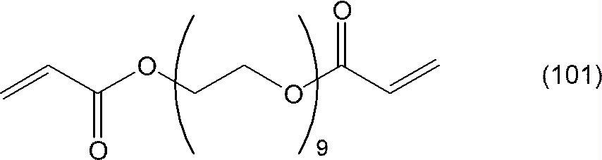
2.前驅物薄膜的製作 以於基板(聚對苯二甲酸乙二醇酯薄膜;NOA CRYSTAL-V,RP TOPLA LIMITED製厚度300μm;玻璃化轉變溫度72℃)上形成厚度0.8μm的底漆層之方式,於基板上塗佈Aica Aitron Z-913-3(Aica Kogyo Co.,Ltd.製),接著對所得到之塗膜照射UV(紫外線)而使塗膜硬化來形成了底漆層。 接著,以於所得到之底漆層上形成厚度0.9 μm的被鍍層前驅物層之方式於底漆層上塗佈被鍍層形成用組成物1而得到附被鍍層前驅物層的基板。2. Fabrication of Precursor Thin Films On the substrate (polyethylene terephthalate film; NOA CRYSTAL-V, manufactured by RP TOPLA LIMITED with a thickness of 300μm; glass transition temperature of 72℃) to form a primer layer with a thickness of 0.8μm Cloth Aica Aitron Z-913-3 (manufactured by Aica Kogyo Co., Ltd.), and then irradiate UV (ultraviolet rays) to the obtained coating film to harden the coating film to form a primer layer. Next, the composition 1 for forming a layer to be plated was coated on the primer layer so as to form a layer to be plated precursor layer with a thickness of 0.9 μm on the obtained primer layer to obtain a substrate with a layer to be plated precursor layer.
3.導電性薄膜的製作
以下的說明中的符號(10、12、14、20、W及L)與圖1或圖2中的符號相同。
(1)曝光處理
接著,使用將所製作之前驅物薄膜剪成15 cm見方者,以形成細線部的寬度W為5 μm,且開口部的一邊長度L為300 μm之網格狀被鍍層12之方式,經由具有規定的圖案之石英遮罩,藉由金屬鹵化物光源對被鍍層前驅物層進行了曝光(0.2 J)。此外,準備複數個將前驅物薄膜剪成15 cm見方者而製備了複數個樣品。
(2)顯影處理
2.1)水顯影
對於1個以上的樣品,使用室溫的水噴淋清洗經曝光處理之被鍍層前驅物層而進行顯影處理,從而製作了具有網格狀被鍍層12之基板(附被鍍層基板)(參閱圖1)。以下,有時將僅用水進行了顯影之附被鍍層基板稱為“附被鍍層基板(水顯影)”。
2.2)鹼顯影
對於另1個以上的樣品,使用3.0質量%碳酸鈉水溶液噴淋清洗經曝光處理之被鍍層前驅物層,接著用室溫的水噴淋清洗被鍍層前驅物層而進行顯影處理,從而製作了具有網格狀被鍍層12之基板(附被鍍層基板)(參閱圖1)。以下,有時將顯影處理時進行了基於碳酸鈉水溶液的清洗之附被鍍層基板稱為“附被鍍層基板(鹼顯影)”。
(3)成形
接著,藉由調溫至90℃之烘箱,將具有直徑10 cm的半球狀凹部之模具加熱了1小時以上。於模具升溫至90℃之後,從烘箱取出模具,並使用耐熱膠帶以覆蓋凹部的開口之方式將所製作之附圖案狀被鍍層基板貼附到模具。將模具快速放回到烘箱,於90℃下將模具放置30秒鐘之後,從位於半球狀凹部的底部的氣孔經5秒鐘進行真空吸引,從而得到了具有半球狀形狀之附被鍍層基板20(參閱圖2)。
(4)電鍍處理
接著,將所得到之具有半球狀形狀之附被鍍層基板(以下,有時簡稱為“附立體形狀被鍍層基板”。)於常溫下在碳酸鈉1質量%水溶液中浸漬5分鐘,並用清水將已取出之附立體形狀被鍍層基板清洗了2次。接著,於純水中浸漬5分鐘之後,於30℃下在Pd觸媒賦予液(Omni shield1573活化劑、Rohm and Haas Electronic Materials製)中浸漬5分鐘,然後用純水將已取出之附立體形狀被鍍層基板清洗了2次。
接著,於30℃下,將所得到之附立體形狀被鍍層基板於還原液(CIRCUPOSIT P13氧化物轉換器60C、Rohm and Haas Electronic Materials製)浸漬5分鐘,然後用純水將已取出之附立體形狀被鍍層基板清洗了2次。
接著,於45℃下,將所得到之附立體形狀被鍍層基板於化學鍍液(CIRCUPOSIT 4500、Rohm and Haas Electronic Materials製)浸漬15分鐘,然後用純水將已取出之附立體形狀被鍍層基板進行清洗,從而得到了具有網格狀金屬層(圖案狀金屬層)且成形為半球狀形狀之導電性薄膜。3. Fabrication of conductive films
Symbols ( 10 , 12 , 14 , 20 , W, and L) in the following description are the same as those in FIG. 1 or FIG. 2 .
(1) Exposure processing
Next, use the method of cutting the prepared precursor film into 15 cm squares to form a grid-shaped layer to be plated 12 with a width W of 5 μm and a length L of one side of the opening of 300 μm. A quartz mask with a prescribed pattern was exposed (0.2 J) to the coating precursor layer by a metal halide light source. In addition, several samples were prepared by cutting the precursor film into 15 cm squares.
(2) Development treatment
2.1) Water development
For one or more samples, the exposed precursor layer to be coated was rinsed with water at room temperature and then developed to produce a substrate with a grid-like coated layer 12 (coated substrate) (see Figure 1). Hereinafter, a substrate to be plated that has been developed only with water may be referred to as a "substrate to be plated (water image development)".
2.2) Alkali development
For the other one or more samples, use 3.0% by mass sodium carbonate aqueous solution to spray and clean the coated precursor layer after exposure treatment, and then spray and clean the coated precursor layer with room temperature water for development treatment, thus making A substrate having a grid-shaped layer to be coated 12 (substrate to be coated) (see FIG. 1 ). Hereinafter, a substrate to be plated that has been washed with an aqueous solution of sodium carbonate during development may be referred to as a "substrate to be plated (alkali development)".
(3) Forming
Next, the mold having the hemispherical concave portion with a diameter of 10 cm was heated for more than 1 hour in an oven whose temperature was adjusted to 90°C. After the mold was heated to 90° C., the mold was taken out from the oven, and the patterned substrate to be plated was attached to the mold using a heat-resistant adhesive tape to cover the opening of the recess. The mold was quickly returned to the oven, and after the mold was placed at 90°C for 30 seconds, vacuum suction was carried out from the air hole at the bottom of the hemispherical concave portion for 5 seconds, thereby obtaining a
4.斷線評價及未曝光部中的銅的析出評價 (1)斷線評價 用光學顯微鏡對成為半球狀形狀之導電性薄膜的斷線進行檢查,並記錄了斷線部位數量。將結果示於表1的“斷線部位數量”的欄中。此外,斷線部位數量表示於半球頂部2 cm見方的區域藉由光學顯微鏡視覺辨認的斷線的數量。 (2)未曝光部中的銅的析出評價 用光學顯微鏡對形成為半球狀形狀之導電性薄膜的未曝光部中的電鍍銅析出區域(以下,有時稱為“異常析出區域”。)進行檢查,並記錄了異常析出區域數量。將結果示於表1的“異常析出區域數量”的欄中。其中,將僅用水進行了顯影者的異常析出區域數量示於“水顯影”的欄中,將用鹼水溶液和水進行了顯影者的異常析出區域數量示於“鹼顯影”的欄中。此外,異常析出區域數量表示於半球頂部2cm見方的區域用光學顯微鏡視覺辨認的異常析出區域的數量。4. Evaluation of disconnection and deposition of copper in unexposed areas (1) Disconnection evaluation The disconnection of the hemispherical conductive film was inspected with an optical microscope, and the number of disconnection sites was recorded. The results are shown in the column of "Number of Disconnection Sites" in Table 1. In addition, the number of broken lines indicates the number of broken lines visually recognized by an optical microscope in a 2 cm square area at the top of the hemisphere. (2) Evaluation of copper deposition in unexposed areas Electroplated copper deposition areas (hereinafter, sometimes referred to as "abnormal deposition areas") in the unexposed portion of the conductive thin film formed in a hemispherical shape were examined with an optical microscope, and the number of abnormal deposition areas was recorded. The results are shown in the column of "Number of Abnormal Precipitation Areas" in Table 1. Among them, the number of abnormal precipitation regions of those developed with water only is shown in the column of "water development", and the number of abnormal precipitation regions of those developed with aqueous alkali solution and water is shown in the column of "alkali development". In addition, the number of abnormal precipitation regions represents the number of abnormal precipitation regions visually recognized with an optical microscope in a 2 cm square area at the top of the hemisphere.
[實施例2] 替代LIGHT ACRYLATE9EG-A而使用了LIGHT ACRYLATE14EG-A(KYOEISHA CHEMICAL Co.,Ltd製;由式(102)表示之化合物;連結鏈長=41;以下,有時簡稱為“14EG-A”。),除此以外,以與實施例1相同的方式進行。[Example 2] Instead of LIGHT ACRYLATE9EG-A, LIGHT ACRYLATE14EG-A (manufactured by KYOEISHA CHEMICAL Co., Ltd; compound represented by formula (102); linking chain length = 41; hereinafter, sometimes abbreviated as "14EG-A" is used.), Except for this, it carried out similarly to Example 1.
[化14]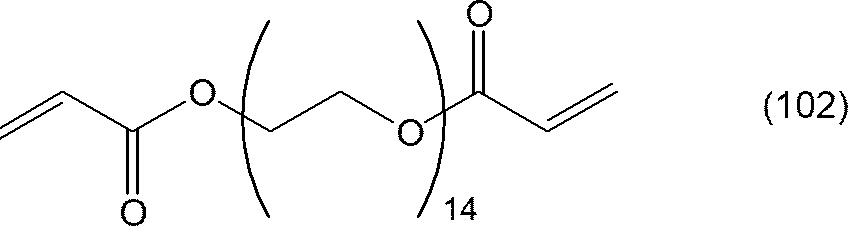
[實施例3] 替代LIGHT ACRYLATE 9EG-A而使用了NK酯A-1000(Shin-Nakamura Chemical Co.,Ltd.製;由式(103)表示之化合物;連結鏈長=68;以下,有時簡稱為“A-1000”。),除此以外,以與實施例1相同的方式進行。[Example 3] Instead of LIGHT ACRYLATE 9EG-A, NK ester A-1000 (manufactured by Shin-Nakamura Chemical Co., Ltd.; a compound represented by formula (103); chain length = 68; hereinafter sometimes referred to as "A- 1000 ".), except that, proceed in the same manner as in Example 1.
[化15]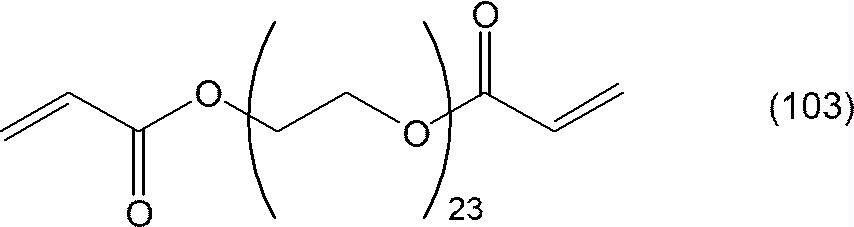
[實施例4] 替代LIGHT ACRYLATE 9EG-A而使用了LIGHT ESTER 9EG(KYOEISHA CHEMICAL Co.,Ltd製;由式(104)表示之化合物;連結鏈長=26;以下有時簡稱為“9EG”。),除此以外,以與實施例1相同的方式進行。[Example 4] Instead of LIGHT ACRYLATE 9EG-A, LIGHT ESTER 9EG (manufactured by KYOEISHA CHEMICAL Co., Ltd; compound represented by formula (104); linking chain length = 26; hereinafter sometimes abbreviated as "9EG") was used, except , in the same manner as in Example 1.
[化16]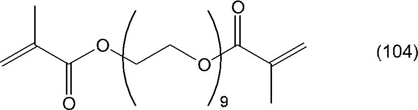
[實施例5] 替代LIGHT ACRYLATE 9EG-A而使用了LIGHT ESTER 14EG(KYOEISHA CHEMICAL Co.,Ltd製;由式(105)表示之化合物;連結鏈長=41;以下,有時簡稱為“14EG”。),除此以外,以與實施例1相同的方式進行。[Example 5] Instead of LIGHT ACRYLATE 9EG-A, LIGHT ESTER 14EG (manufactured by KYOEISHA CHEMICAL Co., Ltd; a compound represented by formula (105); chain length = 41; hereinafter, sometimes abbreviated as "14EG") was used, except Other than that, it carried out in the same manner as Example 1.
[化17]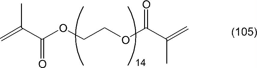
[實施例6] 替代LIGHT ACRYLATE 9EG-A而使用了NK酯23G(Shin-Nakamura Chemical Co.,Ltd.製;由式(106)表示之化合物;連結鏈長=68;以下,有時簡稱為“23G”。),除此以外,以與實施例1相同的方式進行。[Example 6] Instead of LIGHT ACRYLATE 9EG-A, NK ester 23G (manufactured by Shin-Nakamura Chemical Co., Ltd.; compound represented by formula (106); linking chain length = 68; hereinafter, sometimes abbreviated as "23G") was used. , except that, it was carried out in the same manner as in Example 1.
[化18]
[實施例7] 替代IRGACURE OXE02而使用Omnirad127(IGM Resins B.V.製),且將曝光時的光源設為Deep UV燈(USHIO INC.製),除此以外,以與實施例1相同的方式進行。[Example 7] It carried out similarly to Example 1 except having used Omnirad127 (made by IGM Resins B.V.) instead of IRGACURE OXE02, and having used Deep UV lamp (made by USHIO INC.) as the light source at the time of exposure.
[比較例1] 替代LIGHT ACRYLATE 9EG-A而使用了由式(201)表示之2官能丙烯醯胺(連結鏈長=13;按照公開公報2013-502654的[0187]段進行了合成者;以下,有時簡稱為“A”。),除此以外,以與實施例1相同的方式進行。[Comparative example 1] In place of LIGHT ACRYLATE 9EG-A, a bifunctional acrylamide represented by the formula (201) (connection chain length = 13; synthesized according to paragraph [0187] of the publication 2013-502654; hereinafter, sometimes abbreviated as "A".), except that, it carried out in the same manner as Example 1.
[化19]
[比較例2] 替代LIGHT ACRYLATE 9EG-A而使用了LIGHT ACRYLATE 4EG-A(KYOEISHA CHEMICAL Co.,Ltd製;由式(107)表示之化合物;連結鏈長=11;以下,有時簡稱為“4EG-A”。),除此以外,以與實施例1相同的方式進行。[Comparative example 2] Instead of LIGHT ACRYLATE 9EG-A, LIGHT ACRYLATE 4EG-A (manufactured by KYOEISHA CHEMICAL Co., Ltd.; compound represented by formula (107); linking chain length = 11; hereinafter sometimes abbreviated as "4EG-A" was used. ), except that it was carried out in the same manner as in Example 1.
[化20]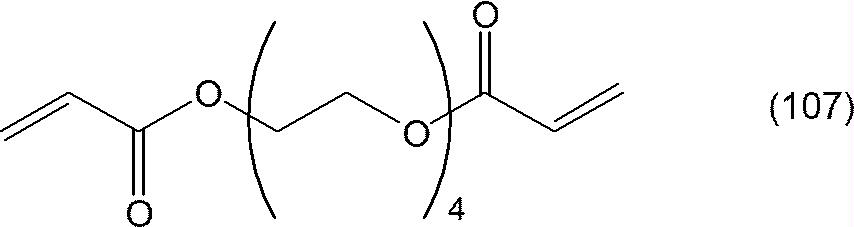
[比較例3] 替代LIGHT ACRYLATE 9EG-A而使用了LIGHT ESTER 4EG(KYOEISHA CHEMICAL Co.,Ltd製;由式(108)表示之化合物;連結鏈長=11;以下,有時簡稱為“4EG”。),除此以外,以與實施例1相同的方式進行。[Comparative example 3] Instead of LIGHT ACRYLATE 9EG-A, LIGHT ESTER 4EG (manufactured by KYOEISHA CHEMICAL Co., Ltd; a compound represented by formula (108); chain length = 11; hereinafter, sometimes abbreviated as "4EG") was used, except Other than that, it carried out in the same manner as Example 1.
[化21]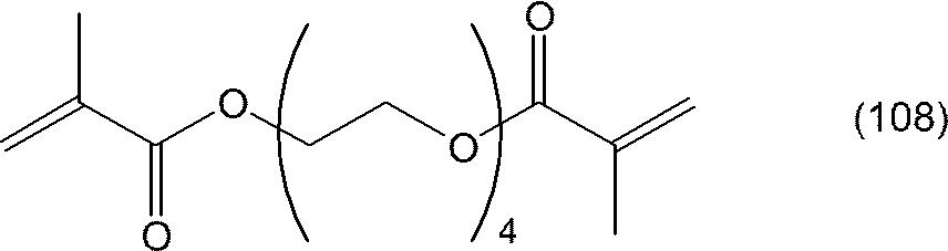
[表1]
[結果的說明] <斷線部位數量> 實施例1~7中,斷線部位數量為0,且被鍍層具有優異的延伸性。 相對於此,比較例1~3中,斷線部位數量為10個部位以上,且被鍍層的延伸性差。 推定其為如下,亦即由於自由基聚合性基團之間的連結鏈長長,即使於90℃這一比以往低的低溫下成形的情況下,被鍍層的延伸性亦充分,且避免了斷線。[explanation of result] <Number of broken wires> In Examples 1 to 7, the number of disconnection sites was 0, and the plated layer had excellent extensibility. On the other hand, in Comparative Examples 1 to 3, the number of disconnection sites was 10 or more, and the stretchability of the to-be-plated layer was poor. It is presumed that due to the length of the linking chain between the radically polymerizable groups, even in the case of molding at a lower temperature of 90°C than before, the elongation of the layer to be plated is sufficient and avoids Disconnected.
<異常析出區域數量> 實施例1~3為,作為2官能單體,使用了連結鏈長不同之2官能丙烯酸酯單體之例。當水顯影時,確認到連結鏈越長,異常析出區域數量越變少之傾向,但當鹼顯影時,未確認到因連結鏈的長度導致的異常析出區域數量的不同,即使連結鏈較短,異常析出區域數量亦為0,且優異。 實施例4~6為,作為2官能單體使用了連結鏈長不同之2官能甲基丙烯酸酯單體之例。與實施例1~3相同,當水顯影時,確認到連結鏈越長,異常析出區域數量越變少之傾向,但當鹼顯影時,未確認到因連結鏈的長度導致的異常析出區域數量的不同,即使連結鏈較短,異常析出區域數量亦為0,且優異。 比較例2及3為,作為2官能單體分別使用了連結鏈長為11的丙烯酸酯單體及連結鏈長為11的甲基丙烯酸酯單體之例。異常析出區域數量越多,越差。作為其理由,首先2官能丙烯酸酯單體及2官能甲基丙烯酸酯單體的氧乙烯的重複單元數越少且疏水性越高,則與底漆層的親和性越變高。因此,認為向底漆層的相互作用性聚合物的浸透得以促進,相互作用性聚合物所浸透之底漆層具有電鍍活性,因此與被鍍層的圖案無關而係因產生被電鍍之部分而引起者。 比較例1為,作為2官能單體而使用了連結鏈長為13的丙烯醯胺單體之例。認為,與2官能丙烯酸酯單體及2官能甲基丙烯酸酯單體相比,丙烯醯胺單體抑制相互作用性聚合物向底漆層的浸透,因此未確認到異常析出區域。<Number of abnormal precipitation areas> Examples 1 to 3 are examples in which bifunctional acrylate monomers having different link chain lengths were used as bifunctional monomers. In the case of water development, it was confirmed that the number of abnormal precipitation regions tended to decrease as the connecting chain became longer. However, in the case of alkali development, the difference in the number of abnormal precipitation regions due to the length of the connecting chain was not confirmed. Even if the connecting chain is short, The number of abnormal precipitation regions was also 0, which was excellent. Examples 4 to 6 are examples in which bifunctional methacrylate monomers having different linking chain lengths were used as bifunctional monomers. As in Examples 1 to 3, when developing with water, it was confirmed that the number of abnormally precipitated regions tended to decrease as the connecting chain became longer, but in the case of alkali developing, the number of abnormally precipitated regions due to the length of the connecting chain was not confirmed. On the other hand, even if the connecting chain is short, the number of abnormally precipitated regions is 0, which is excellent. Comparative Examples 2 and 3 are examples in which an acrylate monomer having a linkage chain length of 11 and a methacrylate monomer having a linkage chain length of 11 were used as bifunctional monomers, respectively. The more the number of abnormal precipitated regions, the worse it is. As the reason, firstly, the smaller the number of repeating units of oxyethylene in the bifunctional acrylate monomer and the bifunctional methacrylate monomer, and the higher the hydrophobicity, the higher the affinity with the primer layer. Therefore, it is considered that the penetration of the interactive polymer into the primer layer is promoted, and the primer layer permeated with the interactive polymer has electroplating activity, so it is caused by the formation of the plated part regardless of the pattern of the plated layer. By. Comparative Example 1 is an example in which an acrylamide monomer having a linkage chain length of 13 was used as a bifunctional monomer. It is considered that the acrylamide monomer inhibits the penetration of the interactive polymer into the primer layer compared with the bifunctional acrylate monomer and the bifunctional methacrylate monomer, so no abnormal precipitation region was confirmed.
10‧‧‧基板
12‧‧‧網格狀被鍍層
14‧‧‧開口部
20‧‧‧具有半球狀形狀之附被鍍層基板
W‧‧‧細線部的線寬
L‧‧‧開口部的一邊的長度10‧‧‧
圖1係具有網格狀被鍍層之基板的頂視圖。 圖2係具有三維形狀之附被鍍層基板的一實施形態的立體圖。Figure 1 is a top view of a substrate with a grid-like coating. Fig. 2 is a perspective view of an embodiment of a plated substrate having a three-dimensional shape.
Claims (19)


Applications Claiming Priority (2)
| Application Number | Priority Date | Filing Date | Title |
|---|---|---|---|
| JP2018-058710 | 2018-03-26 | ||
| JP2018058710 | 2018-03-26 |
Publications (2)
| Publication Number | Publication Date |
|---|---|
| TW201940524A TW201940524A (en) | 2019-10-16 |
| TWI804580B true TWI804580B (en) | 2023-06-11 |
Family
ID=68058515
Family Applications (1)
| Application Number | Title | Priority Date | Filing Date |
|---|---|---|---|
| TW108105674A TWI804580B (en) | 2018-03-26 | 2019-02-20 | Precursor film, substrate with a layer to be plated, conductive film, touch panel sensor, touch panel, a method for producing a conductive film, and a composition for forming a layer to be plated |
Country Status (5)
| Country | Link |
|---|---|
| US (1) | US11123961B2 (en) |
| JP (1) | JP7041741B2 (en) |
| CN (1) | CN111902567B (en) |
| TW (1) | TWI804580B (en) |
| WO (1) | WO2019187709A1 (en) |
Families Citing this family (3)
| Publication number | Priority date | Publication date | Assignee | Title |
|---|---|---|---|---|
| US11936103B2 (en) * | 2019-10-29 | 2024-03-19 | Teijin Limited | Conductive film for antennas, and antenna |
| JP2022029727A (en) * | 2020-08-05 | 2022-02-18 | 三菱電機株式会社 | Antenna built-in touch screen and display apparatus |
| CN113506972A (en) * | 2021-06-08 | 2021-10-15 | 上海宇航系统工程研究所 | Space anti-static film antenna film surface |
Citations (2)
| Publication number | Priority date | Publication date | Assignee | Title |
|---|---|---|---|---|
| TW201623467A (en) * | 2014-09-05 | 2016-07-01 | 日產化學工業股份有限公司 | Photo-curing electroless plating primer |
| WO2018034291A1 (en) * | 2016-08-19 | 2018-02-22 | 富士フイルム株式会社 | Composition for forming plated layer, plated layer, substrate provided with plated layer, electroconductive film, touch panel sensor, and touch panel |
Family Cites Families (15)
| Publication number | Priority date | Publication date | Assignee | Title |
|---|---|---|---|---|
| US5892110A (en) * | 1996-05-21 | 1999-04-06 | Air Products And Chemicals, Inc. | Heterogeneous catalyst for the production of acetic anhydride from methyl acetate |
| TW540284B (en) * | 2001-09-05 | 2003-07-01 | Zeon Corp | Process for manufacturing multi-layer circuit substrate |
| JP5382841B2 (en) * | 2005-10-31 | 2014-01-08 | 日東電工株式会社 | Conductive laminated film, electrode plate for touch panel, touch panel and adhesive for conductive laminated film |
| JP2007234424A (en) * | 2006-03-01 | 2007-09-13 | Nitto Denko Corp | Transparent conductive film and touch panel |
| JP4155315B2 (en) * | 2006-06-28 | 2008-09-24 | オムロン株式会社 | Method for producing metal film, base composition, metal film and use thereof |
| CN102473480B (en) * | 2009-07-08 | 2014-10-08 | 日东电工株式会社 | Transparent conductive film, electronic device, and touch panel |
| ES2768345T3 (en) * | 2011-07-11 | 2020-06-22 | Tokuyama Corp | CURABLE PHOTOCHROMATIC COMPOSITION |
| JP6092035B2 (en) * | 2013-07-30 | 2017-03-08 | 日東電工株式会社 | Surface protective film and optical member |
| US9694338B2 (en) * | 2014-12-18 | 2017-07-04 | Wisconsin Alumni Research Foundation | Covalently-immobilized hydrogel arrays in multi-well plates |
| CN107429400B (en) * | 2015-03-31 | 2019-06-21 | 富士胶片株式会社 | Composition for forming a coating layer, precursor layer film with coating layer, coating layer film with pattern, conductive film, touch panel |
| JP6340378B2 (en) * | 2015-05-11 | 2018-06-06 | 富士フイルム株式会社 | Method for manufacturing conductive laminate, conductive laminate, touch sensor |
| JP6388558B2 (en) * | 2015-05-29 | 2018-09-12 | 富士フイルム株式会社 | Conductive film, touch panel sensor, and touch panel |
| WO2017053803A1 (en) * | 2015-09-23 | 2017-03-30 | Northwestern University | Reprocessable cross-linked network polymers with alkoxyamine dynamic covalent bonds |
| JP6611396B2 (en) * | 2016-03-11 | 2019-11-27 | 富士フイルム株式会社 | Plating layer forming composition, plated layer precursor film, patterned film with plated layer, conductive film, touch panel |
| KR102112435B1 (en) * | 2016-03-23 | 2020-05-18 | 후지필름 가부시키가이샤 | Method of manufacturing a conductive laminate, a three-dimensional structure having a precursor layer to be plated, a three-dimensional structure having a pattern-shaped plated layer, a conductive laminate, a touch sensor, a heating member, and a three-dimensional structure |
-
2019
- 2019-02-12 WO PCT/JP2019/004806 patent/WO2019187709A1/en not_active Ceased
- 2019-02-12 CN CN201980020317.2A patent/CN111902567B/en active Active
- 2019-02-12 JP JP2020510376A patent/JP7041741B2/en not_active Expired - Fee Related
- 2019-02-20 TW TW108105674A patent/TWI804580B/en not_active IP Right Cessation
-
2020
- 2020-09-24 US US17/031,697 patent/US11123961B2/en not_active Expired - Fee Related
Patent Citations (2)
| Publication number | Priority date | Publication date | Assignee | Title |
|---|---|---|---|---|
| TW201623467A (en) * | 2014-09-05 | 2016-07-01 | 日產化學工業股份有限公司 | Photo-curing electroless plating primer |
| WO2018034291A1 (en) * | 2016-08-19 | 2018-02-22 | 富士フイルム株式会社 | Composition for forming plated layer, plated layer, substrate provided with plated layer, electroconductive film, touch panel sensor, and touch panel |
Also Published As
| Publication number | Publication date |
|---|---|
| WO2019187709A1 (en) | 2019-10-03 |
| JPWO2019187709A1 (en) | 2021-03-18 |
| CN111902567A (en) | 2020-11-06 |
| CN111902567B (en) | 2022-10-25 |
| US11123961B2 (en) | 2021-09-21 |
| US20210008841A1 (en) | 2021-01-14 |
| TW201940524A (en) | 2019-10-16 |
| JP7041741B2 (en) | 2022-03-24 |
Similar Documents
| Publication | Publication Date | Title |
|---|---|---|
| JP6340378B2 (en) | Method for manufacturing conductive laminate, conductive laminate, touch sensor | |
| JP6727309B2 (en) | Composition for forming plated layer, plated layer, substrate with plated layer, conductive film, touch panel sensor, touch panel | |
| JP6490194B2 (en) | Plating layer forming composition, plated layer precursor film, patterned film with plated layer, conductive film, touch panel | |
| JPWO2017163830A1 (en) | Manufacturing method of conductive laminate, three-dimensional structure with plated layer precursor layer, three-dimensional structure with patterned layer to be plated, conductive laminate, touch sensor, heating member, and three-dimensional structure | |
| TWI804580B (en) | Precursor film, substrate with a layer to be plated, conductive film, touch panel sensor, touch panel, a method for producing a conductive film, and a composition for forming a layer to be plated | |
| JPWO2018168243A1 (en) | Method for manufacturing conductive laminate, conductive laminate, and touch sensor | |
| JP6275861B2 (en) | Laminated body, conductive laminated body and manufacturing method thereof, touch panel sensor, touch panel, transfer film | |
| CN111902885A (en) | Conductive film, touch panel sensor, and touch panel | |
| TWI795599B (en) | Conductive member, touch panel sensor, touch panel, and method for producing molded article | |
| JP6923749B2 (en) | Conductive film, touch panel sensor, touch panel | |
| WO2020196010A1 (en) | Electroconductive substrate production method | |
| JP7041740B2 (en) | Precursor film, substrate with layer to be plated, conductive film, touch panel sensor, touch panel, method for manufacturing conductive film, and composition for forming layer to be plated. | |
| JP7112591B2 (en) | LAMINATE, METHOD FOR MANUFACTURING SUBSTRATE WITH PLATING LAYER, METHOD FOR MANUFACTURING CONDUCTIVE FILM | |
| JP6951312B2 (en) | Composition for forming a layer to be plated, a substrate with a precursor layer to be plated, a substrate with a layer to be plated, a conductive film, a touch panel sensor, a touch panel | |
| JP7420959B2 (en) | heat generating component | |
| WO2023048204A1 (en) | Laminate production method and laminate |
Legal Events
| Date | Code | Title | Description |
|---|---|---|---|
| MM4A | Annulment or lapse of patent due to non-payment of fees |