TWI854820B - Semiconductor device and manufacturing method thereof - Google Patents
Semiconductor device and manufacturing method thereof Download PDFInfo
- Publication number
- TWI854820B TWI854820B TW112133747A TW112133747A TWI854820B TW I854820 B TWI854820 B TW I854820B TW 112133747 A TW112133747 A TW 112133747A TW 112133747 A TW112133747 A TW 112133747A TW I854820 B TWI854820 B TW I854820B
- Authority
- TW
- Taiwan
- Prior art keywords
- cap layer
- metal cap
- layer
- metal
- dielectric
- Prior art date
Links
Images


Classifications
-
- H—ELECTRICITY
- H10—SEMICONDUCTOR DEVICES; ELECTRIC SOLID-STATE DEVICES NOT OTHERWISE PROVIDED FOR
- H10W—GENERIC PACKAGES, INTERCONNECTIONS, CONNECTORS OR OTHER CONSTRUCTIONAL DETAILS OF DEVICES COVERED BY CLASS H10
- H10W20/00—Interconnections in chips, wafers or substrates
- H10W20/01—Manufacture or treatment
- H10W20/071—Manufacture or treatment of dielectric parts thereof
- H10W20/074—Manufacture or treatment of dielectric parts thereof of dielectric parts comprising thin functional dielectric layers, e.g. dielectric etch-stop, barrier, capping or liner layers
- H10W20/077—Manufacture or treatment of dielectric parts thereof of dielectric parts comprising thin functional dielectric layers, e.g. dielectric etch-stop, barrier, capping or liner layers on sidewalls or on top surfaces of conductors
-
- H—ELECTRICITY
- H10—SEMICONDUCTOR DEVICES; ELECTRIC SOLID-STATE DEVICES NOT OTHERWISE PROVIDED FOR
- H10D—INORGANIC ELECTRIC SEMICONDUCTOR DEVICES
- H10D64/00—Electrodes of devices having potential barriers
- H10D64/01—Manufacture or treatment
- H10D64/013—Manufacture or treatment of electrodes having a conductor capacitively coupled to a semiconductor by an insulator
- H10D64/01302—Manufacture or treatment of electrodes having a conductor capacitively coupled to a semiconductor by an insulator the insulator being formed after the semiconductor body, the semiconductor being silicon
- H10D64/01304—Manufacture or treatment of electrodes having a conductor capacitively coupled to a semiconductor by an insulator the insulator being formed after the semiconductor body, the semiconductor being silicon characterised by the conductor
- H10D64/01326—Aspects related to lithography, isolation or planarisation of the conductor
-
- H—ELECTRICITY
- H10—SEMICONDUCTOR DEVICES; ELECTRIC SOLID-STATE DEVICES NOT OTHERWISE PROVIDED FOR
- H10D—INORGANIC ELECTRIC SEMICONDUCTOR DEVICES
- H10D30/00—Field-effect transistors [FET]
- H10D30/01—Manufacture or treatment
- H10D30/021—Manufacture or treatment of FETs having insulated gates [IGFET]
- H10D30/024—Manufacture or treatment of FETs having insulated gates [IGFET] of fin field-effect transistors [FinFET]
-
- H—ELECTRICITY
- H10—SEMICONDUCTOR DEVICES; ELECTRIC SOLID-STATE DEVICES NOT OTHERWISE PROVIDED FOR
- H10D—INORGANIC ELECTRIC SEMICONDUCTOR DEVICES
- H10D30/00—Field-effect transistors [FET]
- H10D30/60—Insulated-gate field-effect transistors [IGFET]
- H10D30/62—Fin field-effect transistors [FinFET]
- H10D30/6211—Fin field-effect transistors [FinFET] having fin-shaped semiconductor bodies integral with the bulk semiconductor substrates
-
- H—ELECTRICITY
- H10—SEMICONDUCTOR DEVICES; ELECTRIC SOLID-STATE DEVICES NOT OTHERWISE PROVIDED FOR
- H10D—INORGANIC ELECTRIC SEMICONDUCTOR DEVICES
- H10D64/00—Electrodes of devices having potential barriers
- H10D64/01—Manufacture or treatment
- H10D64/011—Manufacture or treatment of electrodes ohmically coupled to a semiconductor
- H10D64/0111—Manufacture or treatment of electrodes ohmically coupled to a semiconductor to Group IV semiconductors
- H10D64/0112—Manufacture or treatment of electrodes ohmically coupled to a semiconductor to Group IV semiconductors using conductive layers comprising silicides
-
- H—ELECTRICITY
- H10—SEMICONDUCTOR DEVICES; ELECTRIC SOLID-STATE DEVICES NOT OTHERWISE PROVIDED FOR
- H10D—INORGANIC ELECTRIC SEMICONDUCTOR DEVICES
- H10D64/00—Electrodes of devices having potential barriers
- H10D64/01—Manufacture or treatment
- H10D64/013—Manufacture or treatment of electrodes having a conductor capacitively coupled to a semiconductor by an insulator
- H10D64/01302—Manufacture or treatment of electrodes having a conductor capacitively coupled to a semiconductor by an insulator the insulator being formed after the semiconductor body, the semiconductor being silicon
- H10D64/01304—Manufacture or treatment of electrodes having a conductor capacitively coupled to a semiconductor by an insulator the insulator being formed after the semiconductor body, the semiconductor being silicon characterised by the conductor
- H10D64/01318—Manufacture or treatment of electrodes having a conductor capacitively coupled to a semiconductor by an insulator the insulator being formed after the semiconductor body, the semiconductor being silicon characterised by the conductor the conductor comprising a layer of alloy material, compound material or organic material contacting the insulator, e.g. TiN
-
- H—ELECTRICITY
- H10—SEMICONDUCTOR DEVICES; ELECTRIC SOLID-STATE DEVICES NOT OTHERWISE PROVIDED FOR
- H10D—INORGANIC ELECTRIC SEMICONDUCTOR DEVICES
- H10D64/00—Electrodes of devices having potential barriers
- H10D64/01—Manufacture or treatment
- H10D64/015—Manufacture or treatment removing at least parts of gate spacers, e.g. disposable spacers
-
- H—ELECTRICITY
- H10—SEMICONDUCTOR DEVICES; ELECTRIC SOLID-STATE DEVICES NOT OTHERWISE PROVIDED FOR
- H10D—INORGANIC ELECTRIC SEMICONDUCTOR DEVICES
- H10D64/00—Electrodes of devices having potential barriers
- H10D64/01—Manufacture or treatment
- H10D64/017—Manufacture or treatment using dummy gates in processes wherein at least parts of the final gates are self-aligned to the dummy gates, i.e. replacement gate processes
-
- H—ELECTRICITY
- H10—SEMICONDUCTOR DEVICES; ELECTRIC SOLID-STATE DEVICES NOT OTHERWISE PROVIDED FOR
- H10D—INORGANIC ELECTRIC SEMICONDUCTOR DEVICES
- H10D64/00—Electrodes of devices having potential barriers
- H10D64/01—Manufacture or treatment
- H10D64/021—Manufacture or treatment using multiple gate spacer layers, e.g. bilayered sidewall spacers
-
- H—ELECTRICITY
- H10—SEMICONDUCTOR DEVICES; ELECTRIC SOLID-STATE DEVICES NOT OTHERWISE PROVIDED FOR
- H10D—INORGANIC ELECTRIC SEMICONDUCTOR DEVICES
- H10D64/00—Electrodes of devices having potential barriers
- H10D64/20—Electrodes characterised by their shapes, relative sizes or dispositions
- H10D64/27—Electrodes not carrying the current to be rectified, amplified, oscillated or switched, e.g. gates
- H10D64/311—Gate electrodes for field-effect devices
- H10D64/411—Gate electrodes for field-effect devices for FETs
- H10D64/511—Gate electrodes for field-effect devices for FETs for IGFETs
- H10D64/517—Gate electrodes for field-effect devices for FETs for IGFETs characterised by the conducting layers
- H10D64/518—Gate electrodes for field-effect devices for FETs for IGFETs characterised by the conducting layers characterised by their lengths or sectional shapes
-
- H—ELECTRICITY
- H10—SEMICONDUCTOR DEVICES; ELECTRIC SOLID-STATE DEVICES NOT OTHERWISE PROVIDED FOR
- H10D—INORGANIC ELECTRIC SEMICONDUCTOR DEVICES
- H10D64/00—Electrodes of devices having potential barriers
- H10D64/60—Electrodes characterised by their materials
- H10D64/66—Electrodes having a conductor capacitively coupled to a semiconductor by an insulator, e.g. MIS electrodes
- H10D64/667—Electrodes having a conductor capacitively coupled to a semiconductor by an insulator, e.g. MIS electrodes the conductor comprising a layer of alloy material, compound material or organic material contacting the insulator, e.g. TiN workfunction layers
-
- H—ELECTRICITY
- H10—SEMICONDUCTOR DEVICES; ELECTRIC SOLID-STATE DEVICES NOT OTHERWISE PROVIDED FOR
- H10D—INORGANIC ELECTRIC SEMICONDUCTOR DEVICES
- H10D64/00—Electrodes of devices having potential barriers
- H10D64/60—Electrodes characterised by their materials
- H10D64/66—Electrodes having a conductor capacitively coupled to a semiconductor by an insulator, e.g. MIS electrodes
- H10D64/671—Electrodes having a conductor capacitively coupled to a semiconductor by an insulator, e.g. MIS electrodes the conductor having lateral variation in doping or structure
Landscapes
- Insulated Gate Type Field-Effect Transistor (AREA)
- Electrodes Of Semiconductors (AREA)
- Chemical & Material Sciences (AREA)
- Composite Materials (AREA)
Abstract
Description
無without
半導體裝置用於諸如(例如)個人電腦、手機、數位相機及其他電子設備的各種電子應用程序中。通常藉由在半導體基板上方按順序沈積絕緣或介電層、導電層及半導體材料層且使用微影術圖案化各種材料層以在其上形成電路元件及部件來製造半導體裝置。 Semiconductor devices are used in a variety of electronic applications such as, for example, personal computers, cell phones, digital cameras, and other electronic devices. Semiconductor devices are typically manufactured by sequentially depositing insulating or dielectric layers, conductive layers, and semiconductor material layers over a semiconductor substrate and patterning the various material layers using lithography to form circuit elements and components thereon.
半導體行業藉由持續縮減最小特徵尺寸來不斷提高各種電子元件(例如電晶體、二極體、電阻器、電容器等)的整合密度,因此能將更多元件整合至給定區域中。然而,隨著最小特徵尺寸的縮減,出現了應解決的額外問題。The semiconductor industry continues to increase the integration density of various electronic components (e.g., transistors, diodes, resistors, capacitors, etc.) by continuously shrinking the minimum feature size, thereby integrating more components into a given area. However, as the minimum feature size shrinks, additional problems arise that should be solved.
無without
以下揭示內容提供了用於實現所提供主題的不同特徵的許多不同實施例或實例。下面描述元件及配置的具體實例係為了簡化本揭露。當然,這些僅僅為實例且不意欲作為限制。 The following disclosure provides many different embodiments or examples for implementing different features of the provided subject matter. Specific examples of components and configurations are described below to simplify the disclosure. Of course, these are merely examples and are not intended to be limiting.
出於簡潔起見,與習知半導體裝置製造相關的習知技術在本文中可不進行詳細描述。此外,本文所述的各種任務及製程可併入具有本文中未詳細描述的額外功能性的更全面的程序或製程中。特定而言,半導體裝置製造中的各種製程為熟知的,因此,出於簡潔起見,許多習知製程將在不提供熟知製程細節的情況下在本文中僅進行簡要提及或將被完全省略。對於熟習此項技術者而言將容易地顯而易見,在完整閱讀本揭露後,本文中所揭示的結構可與各種技術一起使用且可被結合於各種半導體裝置及產品中。另外,應注意,半導體裝置結構包含不同數目的元件,且圖示中所示出的單一元件可代表多個元件。 For the sake of brevity, known techniques related to the manufacture of known semiconductor devices may not be described in detail herein. In addition, the various tasks and processes described herein may be incorporated into more comprehensive procedures or processes having additional functionality not described in detail herein. In particular, various processes in the manufacture of semiconductor devices are well known, and therefore, for the sake of brevity, many known processes will only be briefly mentioned herein or will be omitted entirely without providing the details of the familiar processes. It will be readily apparent to those skilled in the art that, after a complete reading of this disclosure, the structures disclosed herein may be used with various techniques and may be incorporated into various semiconductor devices and products. In addition, it should be noted that semiconductor device structures include different numbers of components and that a single component shown in the diagram may represent multiple components.
此外,為易於描述,在本文中可使用諸如「上方」、「上覆於」、「在……上方」、「上部」、「頂部」、「下方」、「下伏於」、「在……下方」、「下部」、「底部」及類似者的空間相對術語來描述如圖中所說明的一個部件或特徵與另一部件或特徵的關係。除了圖中所描繪的取向之外,空間相對術語亦意欲涵蓋裝置在使用或操作中的不同取向。設備可以其他方式定向(旋轉90度或處於其他取向),且本文中所使用的空間相對描述詞可同樣相應地進行解譯。當空間相對術語(諸如上文所列的空間相對術語)用於相對於第二部件描述第一部件時,第一部件可直接位於另一個部件上,或可存在中間部件或層。當部件或層被稱為「位於」另一部件或層「上」時,該部件或層直接位於另一個部件或層上且與另一個部件或層接觸。 Additionally, for ease of description, spatially relative terms such as "above," "overlying," "above," "upper," "top," "below," "underlying," "beneath," "bottom," and the like may be used herein to describe the relationship of one component or feature to another component or feature as illustrated in the figures. Spatially relative terms are intended to encompass different orientations of the device in use or operation in addition to the orientation depicted in the figures. The apparatus may be otherwise oriented (rotated 90 degrees or in other orientations), and the spatially relative descriptors used herein may be interpreted accordingly. When spatially relative terms (such as the spatially relative terms listed above) are used to describe a first component relative to a second component, the first component may be directly on the other component, or intervening components or layers may be present. When a part or layer is referred to as being "on" another part or layer, the part or layer is directly on and in contact with the other part or layer.
此外,本揭露可在各種實例中重複附圖標記及/或字母。此重複係出於簡單及清楚的目的,且其本身並不表示所論述的各種實施例及/或組態之間的關係。 In addition, the present disclosure may repeat figure labels and/or letters in various examples. This repetition is for the purpose of simplicity and clarity and does not in itself indicate a relationship between the various embodiments and/or configurations discussed.
應注意,說明書中對「一個實施例」、「實施例」、「實例實施例」、「例示性」、「實例」等的引用指示所描述實施例可包含特定特徵、結構或特性,但每個實施例可能並不一定包含特定特徵、結構或特性。此外,此類片語並不一定係指同一實施例。另外,當結合實施例描述特定特徵、結構或特性時,無論是否明確描述,結合其他實施例來影響此特徵、結構或特性將在熟習此項技術者的知識範圍內。 It should be noted that references to "one embodiment", "embodiment", "example embodiment", "exemplary", "example", etc. in the specification indicate that the described embodiment may include specific features, structures or characteristics, but each embodiment may not necessarily include specific features, structures or characteristics. In addition, such phrases do not necessarily refer to the same embodiment. In addition, when a specific feature, structure or characteristic is described in conjunction with an embodiment, whether or not explicitly described, it will be within the knowledge of those skilled in the art to affect this feature, structure or characteristic in conjunction with other embodiments.
應理解,本文中的措辭或術語係出於描述的目的,而非出於限制的目的,使得本說明書的術語或措辭將由熟悉相關技術者鑒於本文中的教導來解譯。 It should be understood that the terms or terminology herein are for descriptive purposes rather than limiting purposes, so that the terms or terminology of this specification will be interpreted by those familiar with the relevant technology in light of the teachings herein.
本文在特定背景(亦即,用於形成包含鰭狀場效電晶體(fin-like field-effect transistor,FinFET)裝置的半導體結構)下論述了各種實施例。半導體結構例如可為互補金屬氧化物半導體(complementary metal-oxide-semiconductor,CMOS)裝置,其包含P型金屬氧化物半導體(P-type metal-oxide-semiconductor,PMOS) FinFET裝置及N型金屬氧化物半導體(N-type metal-oxide-semiconductor,NMOS) FinFET裝置。現將關於包含FinFET製造製程的特定實例描述實施例。然而,實施例不限於本文中所提供的實例,且這些構思可在各種實施例中實現。因此,可將各種實施例應用於其他半導體裝置/製程,諸如平面電晶體及類似者。另外,本文中所論述的一些實施例係在使用後閘極製程形成的裝置的背景下進行論述的。在其他實施例中,可使用前閘極製程。 Various embodiments are discussed herein in a specific context, namely, for forming a semiconductor structure including a fin-like field-effect transistor (FinFET) device. The semiconductor structure may, for example, be a complementary metal-oxide-semiconductor (CMOS) device, which includes a P-type metal-oxide-semiconductor (PMOS) FinFET device and an N-type metal-oxide-semiconductor (NMOS) FinFET device. The embodiments will now be described with respect to a specific example including a FinFET manufacturing process. However, the embodiments are not limited to the examples provided herein, and these concepts may be implemented in a variety of embodiments. Therefore, the various embodiments may be applied to other semiconductor devices/processes, such as planar transistors and the like. Additionally, some of the embodiments discussed herein are discussed in the context of devices formed using a back gate process. In other embodiments, a front gate process may be used.
雖然各圖說明半導體裝置的各種實施例,但可在各圖中所描繪的半導體裝置中添加額外特徵,且可在半導體裝置的其他實施例中替換、修改或消除下面描述的一些特徵。 Although the figures illustrate various embodiments of semiconductor devices, additional features may be added to the semiconductor devices depicted in the figures, and some of the features described below may be replaced, modified, or eliminated in other embodiments of semiconductor devices.
可在這些實施例中所描述的階段之前、期間及/或之後提供額外操作。對於不同實施例,可替換或消除所描述的一些階段。可向半導體裝置結構添加額外特徵。對於不同實施例,可替換或消除下面描述的一些特徵。儘管利用以特定次序執行的操作論述了一些實施例,但可以另一邏輯次序執行這些操作。 Additional operations may be provided before, during, and/or after the stages described in these embodiments. Some of the stages described may be replaced or eliminated for different embodiments. Additional features may be added to the semiconductor device structure. Some of the features described below may be replaced or eliminated for different embodiments. Although some embodiments are discussed with operations performed in a particular order, these operations may be performed in another logical order.
現參考第1A圖,繪示了諸如FinFET裝置的半導體裝置100的透視圖。第1B圖繪示根據一些實施例的沿著剖切線X-X′的第1A圖的橫截面圖。在實施例中,半導體裝置100包括基板101及第一溝槽103。基板101可為矽基板,但亦可使用其他基板,諸如絕緣體上半導體(semiconductor-on-insulator,SOI)、應變SOI及絕緣體上矽鍺。基板101可為p型半導體,但在其他實施例中,其可為n型半導體。
Referring now to FIG. 1A, a perspective view of a
在其他實施例中,基板101可經選擇為將具體地提高由基板101形成的裝置的效能(例如提高載流子遷移率)的材料。舉例而言,在一些實施例中,基板101的材料可經選擇為磊晶生長的半導體材料層,諸如磊晶生長的矽鍺,此有助於提高由磊晶生長的矽鍺形成的裝置的效能的一些量測。然而,雖然使用這些材料可能能夠提高裝置的一些效能特性,但使用這些相同的材料可影響裝置的其他效能特性。舉例而言,使用磊晶生長的矽鍺可降低(相對於矽)裝置的界面缺陷。
In other embodiments,
第一溝槽103可作為最終形成第一隔離區105的初始步驟而形成。可使用掩蔽層(第1A圖中未單獨繪示)連同合適的蝕刻製程來形成第一溝槽103。舉例而言,掩蔽層可為包括經由諸如化學氣相沈積(chemical vapor deposition,CVD)的製程形成的氮化矽的硬遮罩,但可利用諸如氧化物、氮氧化物、碳化矽、這些的組合或類似者的其他材料以及諸如電漿增強化學氣相沈積(plasma enhanced chemical vapor deposition,PECVD)、低壓化學氣相沈積(low pressure chemical vapor deposition,LPCVD)或甚至氧化矽形成,接著為氮化的其他製程。一旦形成,掩蔽層便可經由合適的微影製程而被圖案化,以曝光基板101的將被移除以形成第一溝槽103的那些部分。
The
然而,如熟習此項技術者將認識到的,上述用於形成掩蔽層的製程及材料不係可用於保護基板101的部分,同時曝光基板101的其他部分以形成第一溝槽103的唯一方法。諸如經圖案化及經顯影的光阻劑的任何合適的製程可用於曝光基板101的要移除的部分以形成第一溝槽103。所有此類方法完全意欲包含在本揭露實施例的範疇內。
However, as will be appreciated by those skilled in the art, the above-described processes and materials for forming the masking layer are not the only methods that may be used to protect portions of the
一旦掩蔽層已經形成且經圖案化,第一溝槽103便形成於基板101中。可經由諸如反應離子蝕刻(reactive ion etching,RIE)的合適製程移除所曝光基板101,以便在基板101中形成第一溝槽103,但可使用任何合適的製程。
Once the masking layer has been formed and patterned, the
然而,如一般熟習此項技術者中的一者將認識到的,上述用於形成第一溝槽103的製程僅僅為一種潛在製程且並不意謂唯一實施例。相反,可利用可形成第一溝槽103的任何合適的製程,且可使用任何合適的製程,包含任何數目的掩蔽及移除步驟。
However, as one of ordinary skill in the art will recognize, the process described above for forming the
除了形成第一溝槽103之外,掩蔽及蝕刻製程亦另外由基板101的保持未經移除的那些部分形成鰭片107。這些鰭片107可用於形成多閘極FinFET電晶體的通道區。雖然第1A圖僅繪示由基板101形成的三個鰭片107,但可利用任何數目的鰭片107。
In addition to forming the
此外,可藉由任何合適的方法來圖案化鰭片107。舉例而言,可使用一種或多種微影製程(包含雙圖案化或多圖案化製程)來圖案化鰭片107。一般而言,雙圖案化或多圖案化製程組合了微影及自對準製程,從而允許產生具有例如比可使用單一直接微影製程獲得的間距更小的間距的圖案。舉例而言,在一個實施例中,犧牲層形成於基板上方,且使用微影製程來圖案化該犧牲層。使用自對準製程在經圖案化犧牲層旁邊形成間隔物。接著移除犧牲層,且剩餘間隔物接著可用於圖案化鰭片107。
Furthermore, the
一旦第一溝槽103及鰭片107已經形成,便可用介電材料填充第一溝槽103,且介電材料可凹入於第一溝槽103內以形成第一隔離區105。介電材料可為氧化物材料、高密度電漿(high-density plasma,HDP)氧化物或類似者。在對第一溝槽103進行任選清洗及加襯之後,可使用化學氣相沈積(chemical vapor deposition,CVD)方法(例如HARP製程)、高密度電漿CVD方法或如所屬領域中已知的其他合適的形成方法中任一者來形成介電材料。
Once the
可藉由用介電材料過度填充第一溝槽103及基板101,接著經由諸如化學機械研磨(chemical mechanical polishing,CMP)、蝕刻、這些的組合或類似者的合適製程移除第一溝槽103及鰭片107外部的過量材料來填充第一溝槽103。在實施例中,移除製程亦移除位於鰭片107上方的任何介電材料,使得介電材料的移除將曝光鰭片107的表面以進行進一步的處理步驟。
The
一旦已用介電材料填充了第一溝槽103,介電材料接著便可遠離鰭片107的表面凹陷。可執行凹陷以曝光鰭片107的與鰭片107的頂表面相鄰的側壁的至少一部分。藉由將鰭片107的頂表面浸入諸如HF的蝕刻劑中,可使用濕式蝕刻來使介電材料凹陷,但可使用諸如H
2的其他蝕刻劑以及諸如反應離子蝕刻、利用諸如NH
3/NF
3的蝕刻劑的乾式蝕刻、化學氧化物移除或乾式化學清洗的其他方法。
Once the
然而,如一般熟習此項技術者中的一者將認識到的,上述步驟可僅為用於填充及凹陷介電材料的整個製程流程的一部分。舉例而言,加襯步驟、清洗步驟、退火步驟、間隙填充步驟、這些的組合及類似者亦可用於形成第一溝槽103且用介電材料填充該第一溝槽103。所有潛在製程步驟完全意欲包含在本揭露實施例的範疇內。
However, as one of ordinary skill in the art will recognize, the above steps may be only part of an overall process flow for filling and recessing dielectric material. For example, lining steps, cleaning steps, annealing steps, gap filling steps, combinations of these, and the like may also be used to form the
在第一隔離區105已經形成之後,虛設閘極介電質109、位於虛設閘極介電質109上方的虛設閘極電極111及間隔物113可形成於鰭片107中的每一者上方。在實施例中,可藉由熱氧化、化學氣相沈積、濺射或所屬領域中已知的用於形成閘極介電質的任何其他方法來形成虛設閘極介電質109。取決於閘極介電質形成技術,位於鰭片107頂部的虛設閘極介電質109厚度可與鰭片107的側壁上的閘極介電質厚度不同。
After the
虛設閘極介電質109可包括諸如二氧化矽或氮氧化矽的材料。虛設閘極介電質109可由高介電常數(高k)材料(例如具有大於約5的相對介電常數)形成,該高介電常數材料諸如氧化鑭(La
2O
3)、氧化鋁(Al
2O
3)、氧化鉿(HfO
2)、氮氧化鉿(HfON)或氧化鋯(ZrO
2)或它們的組合。另外,二氧化矽、氮氧化矽及/或高k材料的任何組合亦可用於虛設閘極介電質109。
The dummy gate dielectric 109 may include materials such as silicon dioxide or silicon oxynitride. The dummy gate dielectric 109 may be formed of a high dielectric constant (high-k) material (e.g., having a relative dielectric constant greater than about 5), such as vanadium oxide (La 2 O 3 ), aluminum oxide (Al 2 O 3 ), helium oxide (HfO 2 ), helium oxynitride (HfON), or zirconium oxide (ZrO 2 ) or a combination thereof. In addition, any combination of silicon dioxide, silicon oxynitride, and/or high-k materials may also be used for the
虛設閘極電極111可包括導電或非導電材料且可選自包括多晶矽、W、Al、Cu、AlCu、Ti、TiAlN、TaC、TaCN、TaSiN、Mn、Zr、TiN、Ta、TaN、Co、Ni、這些的組合或類似者的群組。可藉由化學氣相沈積(chemical vapor deposition,CVD)、濺射沈積或所屬領域中已知的用於沈積導電材料的其他技術來沈積虛設閘極電極111。虛設閘極電極111的頂表面可具有非平面的頂表面,且可在虛設閘極電極111的圖案化或閘極蝕刻之前被平坦化。在該點處,離子可或可不被引入至虛設閘極電極111中。舉例而言,藉由離子佈植技術來引入離子。
The
一旦形成,虛設閘極介電質109及虛設閘極電極111可被圖案化以在鰭片107上方形成一系列虛設堆疊115。虛設堆疊115限定位於在虛設閘極介電質109之下的鰭片107的每一側的多個通道區。可藉由使用例如所屬領域中已知的沈積及微影技術在虛設閘極電極111上沈積及圖案化閘極遮罩(第1A圖中未單獨繪示)來形成虛設堆疊115。閘極遮罩可包含通常使用的掩蔽及犧牲材料,諸如(但不限於)氧化矽、氮氧化矽、SiCON、SiC、SiOC及/或氮化矽。可使用乾式蝕刻製程來蝕刻虛設閘極電極111及虛設閘極介電質109,以在虛設堆疊115中形成圖案。
Once formed, the
一旦虛設堆疊115已經圖案化,便可形成間隔物113。間隔物113可形成於虛設堆疊115的相對側。可藉由在先前形成的結構上毯覆沈積一(出於清楚起見,如第1A圖中所繪示)或多個(如第1B圖中所繪示)間隔物層來形成間隔物113。一或多個間隔物層可包括SiN、氮氧化物、SiC、SiON、SiOCN、SiOC、氧化物及類似者且可藉由用於形成此類層的方法來形成,這些方法諸如化學氣相沈積(chemical vapor deposition,CVD)、電漿增強CVD、濺射及所屬領域中已知的其他方法。在具有多於一個間隔物層的實施例中,一或多個間隔物層可使用類似但彼此不同的材料(諸如藉由包括具有不同組分百分比且具有不同固化溫度及孔隙率的材料)以類似方式形成。此外,一或多個間隔物層可包括具有不同蝕刻特性的不同材料或與第一隔離區105內的介電材料相同的材料。接著可諸如藉由一或多種蝕刻來圖案化一或多個間隔物層,從而自結構的水平表面移除一或多個間隔物層。因而,一或多個間隔物層沿著虛設堆疊115的側壁形成且被統稱為間隔物113。
Once the
第1A圖進一步繪示自不受虛設堆疊115及間隔物113保護的那些區域移除鰭片107 (儘管在第1A圖中仍然繪示了鰭片107的位置以示出它們最初所處的位置)以及源極/汲極區117的再生長。單獨或共同取決於上下文,源極/汲極區可指源極或汲極。可藉由使用虛設堆疊115及間隔物113作為硬遮罩的反應離子蝕刻(reactive ion etch,RIE)或藉由任何其他合適的移除製程而自不受虛設堆疊115及間隔物113保護的區域移除鰭片107。移除可繼續,直至鰭片107與第一隔離區105的表面平齊(如所繪示)或低於第一隔離區105的表面為止。
FIG. 1A further illustrates the removal of the
一旦鰭片107的這些部分已經移除,便置放及圖案化硬遮罩(未單獨繪示)以覆蓋虛設閘極電極111,從而防止生長,且源極/汲極區117可再生長為與鰭片107中的每一者接觸。在實施例中,源極/汲極區117可再生長,且在一些實施例中,源極/汲極區117可再生長為形成應力源,該應力源將向鰭片107的位於虛設堆疊115下方的通道區施加應力。在鰭片107包括矽且FinFET為p型裝置的實施例中,源極/汲極區117可經由選擇性磊晶製程用諸如矽的材料或具有與通道區不同的晶格常數的諸如矽鍺的材料再生長。磊晶生長製程可使用前驅物,諸如矽烷、二氯矽烷、鍺烷及類似者,且可持續約5分鐘至約120分鐘,諸如約30分鐘。
Once these portions of the
一旦形成源極/汲極區117,可藉由佈植適合的摻雜劑來將摻雜劑佈植於源極/汲極區117中以補償鰭片107中的摻雜劑。舉例而言,可佈植諸如硼、鎵、銦或類似者的p型摻雜劑來形成PMOS裝置。替代地,可佈植諸如磷、砷、銻或類似者的n型摻雜劑來形成NMOS裝置。可使用虛設堆疊115及間隔物113作為遮罩來佈植這些摻雜劑。應注意,一般熟習此項技術者中的一者將認識到,可使用許多其他製程、步驟或類似者來佈植摻雜劑。舉例而言,一般熟習此項技術者中的一者將認識到,可使用間隔物及襯裡的各種組合來執行複數次佈植,以形成具有適用於特定目的之特定形狀或特性的源極/汲極區。這些製程中的任一者皆可用於佈植摻雜劑,且以上描述並不意謂將本揭露實施例限制於上述步驟。
Once the source/
另外,此時,移除了在形成源極/汲極區117期間覆蓋虛設閘極電極111的硬遮罩。在實施例中,可使用例如對硬遮罩的材料具有選擇性的濕式或乾式蝕刻製程來移除硬遮罩。然而,可利用任何合適的移除製程。
In addition, at this time, the hard mask covering the
第1A圖亦繪示在虛設堆疊115及源極/汲極區117上方形成第一層間介電(interlayer dielectric,ILD)層119 (在第1A圖中用虛線示出,以便更清楚地繪示下伏結構)。第一ILD層119可包括諸如硼磷矽玻璃(boron phosphorous silicate glass,BPSG)的材料,但可使用任何合適的介電質。可使用諸如PECVD的製程來形成第一ILD層119,但替代地,亦可使用諸如LPCVD的其他製程。一旦形成,第一ILD層119便可使用例如諸如化學機械研磨製程的平坦化製程與間隔物113平坦化,但可利用任何合適的製程。
FIG. 1A also shows a first interlayer dielectric (ILD)
第2圖繪示用於在半導體裝置中形成金屬閘極的實例製程200的製程流程圖,該金屬閘極包含閘極堆疊、安置於該閘極堆疊上方的金屬帽及安置於該金屬帽上方的介電層(諸如氮化矽(silicon nitride,SiN))。結合第3A圖至第3K圖描述了第2圖,該第3A圖至該第3K圖為半導體裝置的橫截面圖,其繪示根據實例製程200的本揭露的一些實施例的在各個製造階段的半導體裝置。實例製程200僅僅為實例且不意欲將本揭露限制在申請專利範圍中明確敘述的內容之外。可在實例製程200之前、期間及之後提供額外步驟,且對於實例製程200的額外實施例,可移動、替換或消除所描述的一些步驟。可在各圖中所描繪的半導體裝置中添加額外特徵,且可在半導體裝置的其他實施例中替換、修改或消除下面描述的一些特徵。
FIG. 2 is a process flow diagram of an
應理解,可藉由典型的半導體技術製程流程來製造半導體裝置的部分,因此本文中僅對一些製程進行簡要描述。另外,例示性半導體裝置可包含各種其他裝置及特徵,諸如其他類型的裝置,諸如額外電晶體、雙極接面電晶體、電阻器、電容器、電感器、二極體、保險絲及/或其他邏輯裝置等,但為了更佳地理解本揭露的構思而被簡化。在一些實施例中,例示性裝置包含可互連的複數個半導體裝置(例如電晶體),包含PFET、NFET等。此外,應注意,實例製程200的操作(包含參考各圖給定的任何描述)僅僅為例示性的,且並不意欲限制在所附申請專利範圍中具體敘述的內容之外。 It should be understood that portions of a semiconductor device may be manufactured using typical semiconductor technology process flows, and therefore only some processes are briefly described herein. In addition, the exemplary semiconductor device may include various other devices and features, such as other types of devices, such as additional transistors, bipolar junction transistors, resistors, capacitors, inductors, diodes, fuses, and/or other logic devices, but are simplified for a better understanding of the concepts of the present disclosure. In some embodiments, the exemplary device includes a plurality of semiconductor devices (e.g., transistors) that may be interconnected, including PFETs, NFETs, and the like. Furthermore, it should be noted that the operations of example process 200 (including any description given with reference to the various figures) are merely illustrative and are not intended to be limited beyond those specifically described in the attached claims.
第3A圖至第3K圖繪示根據一些實施例的在製造半導體裝置的各個階段的實例區域300 (及實例區域300的子區域301)的放大視圖的圖式。在一些圖中,可省略這些圖中所繪示的元件或特徵的一些附圖標記,以免模糊其他元件或特徵;這係為了便於描繪各圖。
Figures 3A to 3K illustrate enlarged views of example region 300 (and
在方塊202中,實例製程200包含自基板移除虛設閘極。可藉由合適的蝕刻製程來移除虛設閘極電極及/或閘極介電質。參考第3A圖及第3B圖的實例,在方塊202的實施例中,實例區域300及子區域301包含具有藉由移除虛設閘極形成的開口304的基板302。在一些實施例中,基板302可為半導體基板,諸如矽基板。基板302可包含各種層,其包含形成於半導體基板上的導電或絕緣層。取決於如所屬領域中已知的設計要求,基板302可包含各種摻雜組態。舉例而言,可在為不同裝置類型(例如n型場效電晶體(n-type field effect transistor,NFET)、p型場效電晶體(p-type field effect transistor,PFET))設計的區中的基板302上形成不同摻雜分佈(例如n井、p井)。合適的摻雜可包含摻雜劑的離子佈植及/或擴散製程。基板302通常具有插入提供不同裝置類型的區的隔離特徵(例如淺溝槽隔離(shallow trench isolation,STI)特徵)。基板302亦可包含其他半導體,諸如鍺、碳化矽(SiC)、矽鍺(SiGe)或金剛石。替代地,基板302可包含化合物半導體及/或合金半導體。另外,基板302可任選地包含磊晶層(epi層),可經應變以實現效能增強,可包含絕緣體上矽(silicon-on-insulator,SOI)結構及/或具有其他合適的增強特徵。
In
子區域301進一步包含一或多個間隔物層306。在該實例中,一或多個間隔物層306包含第一間隔物層306a (諸如蝕刻終止層)、第二間隔物層306b及第三間隔物層306c。一或多個間隔物層可包括SiO
2、SiN、SiOC、氧氮化物、SiC、SiON、SiOCN、氧化物及類似者,且可藉由用於形成此類層的方法來形成,這些方法諸如化學氣相沈積(chemical vapor deposition,CVD)、電漿增強CVD、濺射及所屬領域中已知的其他方法。
The
子區域301進一步包含位於源極/汲極區310上方的層間介電(ILD0)層308及位於該ILD0層308上方的第二介電層312。ILD0層308可包括氧化物或諸如硼磷矽玻璃(boron phosphorous silicate glass,BPSG)的材料,但可使用任何合適的介電質。第二介電層312可包括諸如SiN或SiOCN的材料,但可使用任何合適的介電質。可使用諸如PECVD的製程來形成ILD0層308及/或第二介電層312,但替代地,可使用諸如LPCVD的其他製程。
在方塊204中,實例製程200包含在基板302上方的開口304中形成界面層(interfacial layer,IL)及位於該IL上方的高K材料介電層。可藉由化學氧化、熱氧化、原子層沈積(atomic layer deposition,ALD)、化學氣相沈積(chemical vapor deposition,CVD)及/或其他合適的方法來形成界面層。可藉由ALD、物理氣相沈積(physical vapor deposition,PVD)、CVD、氧化及/或其他合適的方法來形成高K閘極介電層。
In
在方塊206中,實例製程200包含形成一或多種功函數金屬。可藉由CVD、ALD及/或其他合適的製程來形成一或多種功函數金屬層。
In
參考第3C圖的實例,在方塊204及206的實施例中,實例子區域301包含沈積於IL (未示出)上方的高K材料介電層314、沈積於高K材料介電層314上方的第一功函數金屬層316、沈積於第一功函數金屬層316上方的第二功函數金屬層318及沈積於第二功函數金屬層318上方的第三功函數金屬層320。
Referring to the example of FIG. 3C , in the embodiment of
在一些實施例中,界面層可包含介電材料,諸如氧化矽(SiO 2)、HfSiO或氮氧化矽(SiON)。可藉由化學氧化、熱氧化、原子層沈積(atomic layer deposition,ALD)、化學氣相沈積(chemical vapor deposition,CVD)及/或其他合適的方法來形成界面層。 In some embodiments, the interface layer may include a dielectric material such as silicon oxide (SiO 2 ), HfSiO, or silicon oxynitride (SiON). The interface layer may be formed by chemical oxidation, thermal oxidation, atomic layer deposition (ALD), chemical vapor deposition (CVD), and/or other suitable methods.
如本文中所使用及描述的,高K閘極介電質包含具有高介電常數(例如大於熱氧化矽的介電常數(約3.9))的介電材料。高K材料介電層314可包含高K介電層,諸如氧化鉿(HfO
2)。替代地,高K閘極介電層可包含其他高K介電質,諸如TiO
2、HfZrO、Ta
2O
3、HfSiO
4、ZrO
2、ZrSiO
2、LaO、AlO、ZrO、TiO、Ta
2O
5、Y
2O
3、SrTiO
3(STO)、BaTiO
3(BTO)、BaZrO、HfZrO、HfLaO、HfSiO、LaSiO、AlSiO、HfTaO、HfTiO、(Ba,Sr)TiO
3(BST)、Al
2O
3、Si
3N
4、氮氧化物(SiON)、它們的組合或其他合適的材料。可藉由ALD、物理氣相沈積(physical vapor deposition,PVD)、CVD、氧化及/或其他合適的方法來形成高K材料介電層314。
As used and described herein, a high-K gate dielectric includes a dielectric material having a high dielectric constant, such as greater than the dielectric constant of thermal silicon oxide (about 3.9). The high-K
在一些實施例中,第一功函數金屬層316及第二功函數金屬層318可包括用於調諧p型電晶體的臨限值電壓的p型功函數金屬。在一些實施例中,第三功函數金屬層320可包括用於調諧n型電晶體的臨限值電壓的n型功函數金屬。第一功函數金屬層316及第二功函數金屬層318可包含過渡金屬,諸如TiN、TaN、WCN或任何合適的材料或它們的組合。第三功函數金屬層320可包含過渡金屬,諸如TiAlC、TaAlC或任何合適的材料或它們的組合。
In some embodiments, the first work
在方塊208中,實例製程200包含形成閘極電極層。可藉由CVD、ALD及/或其他合適的製程來形成閘極電極層。參考第3D圖的實例,在方塊208的實施例中,實例子區域301包含沈積於第三功函數金屬層320上方的閘極電極層322。閘極電極層322可包括諸如TiN的材料或任何合適的材料或它們的組合。
In
在方塊210中,實例製程200包含形成第一金屬帽層。可藉由CVD、ALD及/或其他合適的製程來形成第一金屬帽層。參考第3E圖的實例,在方塊210的實施例中,實例子區域301包含沈積於閘極電極層322上方的第一金屬帽層324。第一金屬帽層324可包括諸如鎢(W)的金屬或任何合適的材料或它們的組合。
In
在方塊212中,實例製程200包含形成介電閘極帽層。可藉由CVD、ALD及/或其他合適的製程來形成介電閘極帽層。參考第3F圖的實例,在方塊212的實施例中,實例子區域301包含沈積於第一金屬帽層324上方的第一介電閘極帽層326。第一介電閘極帽層326可包括諸如氮化矽(SiN)的材料、氧化物或任何合適的材料或它們的組合。
In
在方塊214中,實例製程200包含在金屬閘極回蝕操作期間,將高K材料介電層、一或多個功函數金屬層、閘極電極層及第一金屬帽層的一部分選擇性地移除至高於第一金屬帽層的底表面且低於第一金屬帽層的主體部分的頂表面的層級。選擇性地移除一或多個功函數金屬層、閘極電極層及第一金屬帽層,以使第一金屬帽層的一部分保留在介電閘極帽層的側壁上。
In
參考第3G圖的實例,在方塊214的實施例中,已將高K材料介電層314、一或多個功函數金屬層(例如第一功函數金屬層316、第二功函數金屬層318及第三功函數金屬層320)、閘極電極層322及第一金屬帽層324的一部分選擇性地移除至高於第一金屬帽層324的底表面(324a)且低於第一金屬帽層324的主體部分的頂表面(324b)的層級。在金屬閘極回蝕操作期間已選擇性地移除了高K材料介電層314、一或多個功函數金屬層、閘極電極層322及第一金屬帽層324,以使第一金屬帽層324的側壁部分324c保留在介電閘極帽層的側壁上。第一金屬帽層324的這些側壁部分324c可防止在半導體結構的進一步處理期間形成缺陷,諸如在半導體結構的進一步處理期間將第一介電閘極帽層326移位或移動至非所需位置。
Referring to the example of FIG. 3G , in the embodiment of
高K材料介電層314、一或多個功函數金屬層(例如第一功函數金屬層316、第二功函數金屬層318及第三功函數金屬層320)、閘極電極層322及第一金屬帽層324可在金屬閘極回蝕操作期間經由濕式蝕刻操作、乾式蝕刻操作或濕式蝕刻操作及乾式蝕刻操作的組合而被選擇性地移除。
The high-K
在各種實施例中,可藉由在液體儲槽中用蝕刻溶液浸漬、浸沒或浸泡基板來執行濕式蝕刻操作。在各種實施例中,在濕式蝕刻操作期間,化學蝕刻劑為包括在約20℃至約70℃的溫度下具有約1:1:360至約1:1:5的濃度比範圍的氯化氫(HCl)、過氧化氫(H 2O 2)及水(H 20)的溶液。 In various embodiments, a wet etching operation can be performed by dipping, immersing or soaking the substrate with an etching solution in a liquid tank. In various embodiments, during the wet etching operation, the chemical etchant is a solution including hydrogen chloride (HCl), hydrogen peroxide ( H2O2 ) and water ( H2O ) having a concentration ratio ranging from about 1:1:360 to about 1: 1 :5 at a temperature of about 20°C to about 70°C.
在各種實施例中,可在電漿乾式蝕刻腔室中執行乾式蝕刻操作。在各種實施例中,在乾式蝕刻操作期間,使用包括諸如BCl 3及/或Cl 2的蝕刻氣體的氣源來完成蝕刻。在各種實施例中,在約0 sccm (標準立方釐米每分鐘)至約1000 sccm之間施用蝕刻氣體。在各種實施例中,以自約1.5毫托至約300毫托的腔室壓力、自約300 W至約1000 W的源功率及自約0 W至約100 W的偏置功率施用蝕刻氣體。 In various embodiments, a dry etching operation can be performed in a plasma dry etching chamber. In various embodiments, during the dry etching operation, etching is performed using a gas source including an etching gas such as BCl 3 and/or Cl 2. In various embodiments, the etching gas is applied between about 0 sccm (standard cubic centimeters per minute) and about 1000 sccm. In various embodiments, the etching gas is applied at a chamber pressure from about 1.5 mTorr to about 300 mTorr, a source power from about 300 W to about 1000 W, and a bias power from about 0 W to about 100 W.
在方塊216中,實例製程200包含在高K材料介電層、一或多個功函數金屬層、閘極電極層及第一金屬帽層上方形成第二金屬帽層。可藉由CVD、ALD及/或其他合適的製程來形成第二金屬帽層。可添加第二金屬帽層以形成組合金屬帽,該組合金屬帽在一或多種間隔物之間且跨高K材料介電層、一或多個功函數金屬層、閘極電極層及第一金屬帽層的頂部伸展。
In
參考第3H圖的實例,在方塊216的實施例中,第二金屬帽層328已形成於高K材料介電層314、一或多個功函數金屬層(例如第一功函數金屬層316、第二功函數金屬層318及第三功函數金屬層320)、閘極電極層322及第一金屬帽層324上方。第二金屬帽層328可包括諸如鎢(W)的金屬或任何合適的材料或它們的組合。第二金屬帽層328形成組合金屬帽,該組合金屬帽在一或多個間隔物層306之間且跨高K材料介電層314、一或多個功函數金屬層(例如第一功函數金屬層316、第二功函數金屬層318及第三功函數金屬層320)、閘極電極層322及第一金屬帽層324的頂部伸展。
3H, in the embodiment of
作為形成於第一金屬帽層324上方的第二金屬帽層328的結果,形成了如第3K圖中所繪示的組合金屬帽層330。在各種實施例中,組合金屬帽層330具有內部位置(例如與組合介電帽層340的內側壁349鄰接的側壁部分347)處的長度L
inner332,邊緣長度L
outer334及在L
inner332與L
outer334之間的點處的長度L
mid336,其中L
outer在約1 nm至約10 nm之間,L
mid在約1 nm至約10 nm之間,L
inner在約2 nm至約15 nm之間,L
inner/ L
outer大於1.5,且L
inner/ L
mid大於1.5。
As a result of forming the second
在方塊218中,實例製程200包含在第二金屬帽層上方形成額外介電閘極帽層。可藉由CVD、ALD及/或其他合適的製程來沈積額外介電閘極帽層338。參考第3I圖的實例,額外介電閘極帽層338已形成於第二金屬帽層328上方。額外介電閘極帽層338可包括諸如氮化矽(SiN)、氧化物或任何合適的材料或它們的組合的材料。額外介電閘極帽層338與第一介電閘極帽層326一起形成組合介電閘極帽(例如,如第3K圖中所繪示的組合介電帽層340),該組合介電閘極帽在一或多個間隔物層306之間且跨第二金屬帽層328的頂部伸展。
In
在方塊220中,實例製程200包含移除過量的介電閘極帽材料。此可使用諸如化學機械(chemical mechanical,CMP)操作的平坦化操作來執行。參考第3J圖的實例,在方塊220的實施例中,一個製造階段的子區域301經描繪為具有沈積於基板302的主動區上方的閘極堆疊(例如高K材料介電層314、第一功函數金屬層316、第二功函數金屬層318、第三功函數金屬層320及閘極電極層322)、組合金屬帽(例如第一金屬帽層324及第二金屬帽層328)及組合介電閘極帽(例如第一介電閘極帽層326及額外介電閘極帽層338)。介電閘極帽及間隔物層306已經平坦化至所需高度。
The
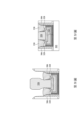
第3K圖提供在第3J圖中所描繪的製造階段的子區域301的另一視圖。第3K圖描繪了沈積於基板302的主動區上方的閘極堆疊342 (例如高K材料介電層314、第一功函數金屬層316、第二功函數金屬層318、第三功函數金屬層320及閘極電極層322)、組合金屬帽層330 (例如第一金屬帽層324及第二金屬帽層328)及組合介電帽層340 (例如第一介電閘極帽層326及額外介電閘極帽層338)。組合介電帽層340及間隔物層306已經平坦化至所需高度。
FIG. 3K provides another view of the
在該實例中,組合介電帽層340的底部邊緣341在組合金屬帽層330的部分下方延伸。組合介電帽層340的底部部分343在組合金屬帽層330的頂部邊緣部分345下方延伸一距離。
In this example, a
在方塊222中,實例製程200包含繼續半導體裝置的半導體製造。此外,實例製程200中未描述的額外製造操作可在實例製程200中所包含的方塊202至220之前、之間及之後發生。
In
半導體裝置可經歷進一步的處理以形成所屬領域中已知的各種特徵及區。舉例而言,後續處理可在基板上形成用以連接各種特徵以形成可包含一或多個多閘極裝置的功能電路的接觸開口、接觸金屬以及各種觸點/通孔/線及多層互連特徵(例如金屬層及層間介電質)。為了促進實例,多層互連可包含諸如通孔或觸點的垂直互連及諸如金屬線的水平互連。各種互連特徵可採用各種導電材料,其包含銅、鎢及/或矽化物。在一個實例中,鑲嵌及/或雙鑲嵌製程用於形成銅相關的多層互連結構。 The semiconductor device may undergo further processing to form various features and regions known in the art. For example, subsequent processing may form contact openings, contact metals, and various contacts/vias/lines and multi-layer interconnect features (e.g., metal layers and interlayer dielectrics) on the substrate for connecting various features to form functional circuits that may include one or more multi-gate devices. To facilitate the example, the multi-layer interconnects may include vertical interconnects such as vias or contacts and horizontal interconnects such as metal lines. The various interconnect features may employ various conductive materials including copper, tungsten, and/or silicide. In one example, damascene and/or dual damascene processes are used to form copper-related multi-layer interconnect structures.
第4圖繪示根據一些實施例的半導體製造的實例方法400的製程流程圖,該半導體製程包含在金屬閘極形成之後的金屬汲極(metal drain,MD)製造及通孔閘極(via gate,VG)製造。方法400僅僅為實例且不意欲將本揭露限制在申請專利範圍中明確敘述的內容之外。可在方法400之前、期間及之後提供額外步驟,且對於方法400的額外實施例,可移動、替換或消除所描述的一些步驟。可在圖中所描繪的積體電路中添加額外特徵,且在其他實施例中可替換、修改或消除下面描述的一些特徵。
FIG. 4 illustrates a process flow diagram of an
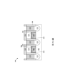
結合第5A圖至第5E圖描述了第4圖,其中第5A圖至第5E圖繪示根據一些實施例的在包含金屬汲極製造及通孔閘極製造的半導體製造的各個階段的實例區域500的放大視圖的圖式。在一些圖中,可省略這些圖中所繪示的元件或特徵的一些附圖標記,以免模糊其他元件或特徵;這係為了便於描繪各圖。
FIG. 4 is described in conjunction with FIGS. 5A to 5E, wherein FIGS. 5A to 5E illustrate diagrams of enlarged views of an
在方塊402中,實例方法400包含設置基板,該基板具有金屬閘極、位於金屬閘極的側部的閘極間隔物、形成於金屬閘極上方的金屬帽、蝕刻終止層(etch stop layer,ESL)及位於源極/汲極區上方的層間介電(interlayer dielectric,ILD)材料。
In
在方塊404中,實例方法400包含在金屬帽上方形成第一ILD層。第一ILD層可包含或可為諸如氮化矽(SiN)的材料,但亦可利用其他合適的材料,諸如氧化矽(SiO
2)、氧化鋁(AlO)、碳氧化矽(SiOC)、碳化矽(SiC)、氮化鋯(ZrN)、氧化鋯(ZrO)、這些的組合或類似者。可使用諸如電漿增強原子層沈積(plasma enhanced atomic layer deposition,PEALD)、熱原子層沈積(熱ALD)、電漿增強化學氣相沈積(plasma enhanced chemical vapor deposition,PECVD)或其他製程的沈積製程來沈積第一ILD層。可利用任何合適的沈積製程及製程條件。
At
在方塊406中,實例方法400包含在源極/汲極區上方形成曝光ILD材料的一部分的經圖案化遮罩。經圖案化遮罩可包含光阻劑層。可藉由光阻劑塗佈(例如旋塗)、軟烘烤、遮罩對準、曝光、曝光後烘烤、顯影光阻劑、沖洗、乾燥(例如硬烘烤)及/或它們的組合來形成經圖案化遮罩。在一些其他實施例中,可在光阻劑層下方形成各種成像增強層以增強圖案轉印。成像增強層可包括三層,包含底部有機層、中間無機層及頂部有機層。成像增強層亦可包含抗反射塗層(anti-reflective coating,ARC)材料、聚合物層、源自TEOS (正矽酸乙酯)的氧化物、氧化矽或含矽抗反射塗層(anti-reflective coating,ARC)材料,諸如含42%矽的ARC層。在又一些其他實施例中,經圖案化遮罩層包含硬遮罩層。硬遮罩層包含氧化物材料、氮化矽、氮氧化矽、無定形碳材料、碳化矽或正矽酸乙酯(tetraethylorthosilicate,TEOS)。In
參考第5A圖的實例,在完成方塊402、404及406之後的實施例中,繪示了包含基板501的區域500,該基板501具有金屬閘極堆疊502、位於金屬閘極堆疊502的側部的閘極間隔物504、形成於金屬閘極堆疊502上方的金屬帽506、蝕刻終止層(etch stop layer,ESL) 508、位於源極/汲極區512上方的ILD材料510、位於金屬帽506上方的第一ILD層514及經圖案化遮罩516,該經圖案化遮罩516曝光位於源極/汲極區512上方的ILD材料510的一部分。
Referring to the example of FIG. 5A , in an embodiment after completing
在方塊408中,實例方法400包含移除位於源極/汲極區上方的ILD材料以形成曝光下伏源極/汲極區的開口。可藉由諸如濕式蝕刻、乾式蝕刻或它們的組合的合適的蝕刻製程來移除ILD材料的曝光部分。
At
在方塊410中,實例方法400包含在已經曝光的源極/汲極區上任選地形成矽化物觸點。任選矽化物觸點可包括鈦(例如矽化鈦(TiSi)),以便降低觸點的肖特基(Schottky)阻障高度。然而,亦可使用其他金屬,諸如鎳、鈷、鉺、鉑、鈀及類似者。可藉由適合的金屬層的毯覆沈積,接著為退火步驟來執行矽化,該退火步驟使金屬與源極/汲極區的下伏曝光矽反應。
At
參考第5B圖的實例,在完成方塊408及410之後的實施例中,區域500包含開口518,該些開口518曝光下伏源極/汲極區512及在已曝光的源極/汲極區512上任選地形成的矽化物觸點520。各圖描繪了已移除位於源極/汲極區512上方的ILD材料510,以形成曝光下伏源極/汲極區512的開口518。
Referring to the example of FIG. 5B , in an embodiment after completing
在方塊412中,實例方法400包含在接觸源極/汲極區的開口中填充導電材料以形成源極/汲極觸點。源極/汲極觸點可包括一或多個層。舉例而言,在一些實施例中,源極/汲極觸點包括藉由例如CVD、ALD、無電沈積(electroless deposition,ELD)、PVD、電鍍或另一沈積技術沈積的襯裡及金屬填充材料(未單獨示出)。諸如擴散阻障層、黏附層或類似者的襯裡可包含鈦、氮化鈦、鉭、氮化鉭或類似者。導電材料可為銅、銅合金、銀、金、鎢、鈷、鋁、釕、鎳或類似者。可執行諸如CMP的平坦化製程以移除過量的襯裡及導電材料。剩餘襯裡及導電材料在開口中形成源極/汲極觸點。
At
參考第5C圖的實例,在完成方塊412之後的實施例中,區域500包含填充開口518且接觸源極/汲極區512以形成源極/汲極觸點522的導電材料。
Referring to the example of FIG. 5C , in an embodiment after completing
在方塊414中,實例方法400包含在源極/汲極及閘極區上方形成接觸蝕刻終止層(contact etch stop layer,CESL)。可使用諸如化學氣相沈積、物理氣相沈積或原子層沈積的一或多種低溫沈積製程來沈積CESL。
At
在方塊416中,實例方法400包含在CESL層上方形成第二ILD層。第二ILD層可由諸如氧化物(例如氧化矽(SiO
2))的介電材料形成,且可藉由任何可接受的製程(例如CVD、PEALD、熱ALD、PECVD或類似者)沈積於CESL上方。第二ILD層亦可由其他合適的絕緣材料(例如PSG、BSG、BPSG、USG或類似者)形成,這些絕緣材料藉由任何合適的方法(例如CVD、PECVD、可流動CVD或類似者)沈積。在形成之後,可諸如藉由紫外線固化製程來使第二ILD層固化。
At
參考第5D圖的實例,在完成方塊414及416之後的實施例中,區域500包含形成於源極/汲極及閘極區上方的CESL層524以及形成於CESL層524上方的第二ILD層526。
Referring to the example of FIG. 5D , in an embodiment after completing
在方塊418中,實例方法400包含在CESL及第二ILD層中形成用於閘極通孔觸點及源極/汲極通孔觸點的接觸通孔開口。經由使用一或多種蝕刻製程來形成用於閘極通孔觸點及源極/汲極通孔觸點的接觸通孔開口。根據一些實施例,經由第二ILD層、CESL及第一ILD層形成用於閘極通孔觸點的開口,且經由第二ILD層及CESL形成用於源極/汲極通孔觸點的開口。可使用可接受的微影及合適的蝕刻技術的任何組合來形成開口,這些蝕刻技術諸如乾式蝕刻製程(例如電漿蝕刻、反應離子蝕刻(reactive ion etch,RIE)、物理蝕刻(例如離子束蝕刻(ion beam etch,IBE)))、濕式蝕刻、它們的組合及類似者。然而,可利用任何合適的蝕刻製程來形成接觸通孔開口。
At
在方塊420中,實例方法400包含形成通孔閘極觸點及源極/汲極通孔觸點。閘極通孔觸點形成於金屬帽上方且電耦接至金屬帽,且源極/汲極通孔觸點形成於源極/汲極觸點上方且電耦接至源極/汲極觸點。可藉由將金屬材料沈積於開口中來形成通孔閘極觸點及/或源極/汲極通孔觸點。可藉由CVD、ALD、無電沈積(electroless deposition,ELD)、PVD、電鍍或另一沈積技術來沈積金屬材料。通孔閘極觸點及/或源極/汲極通孔觸點可為或包括鎢、鈷、銅、釕、鋁、金、銀、它們的合金、類似者或它們的組合。
At
參考第5E圖的實例,在完成方塊418及420之後的實施例中,區域500包含通孔閘極觸點528及源極/汲極通孔觸點(未示出)。
Referring to the example of FIG. 5E , in an embodiment after completing
在方塊422中,實例方法400包含執行進一步的製造操作。半導體裝置可經歷進一步的處理以形成所屬領域中已知的各種特徵及區。舉例而言,後續處理可在基板上形成用以連接各種特徵以形成可包含一或多個多閘極裝置的功能電路的各種觸點/通孔/線及多層互連特徵(例如金屬層及層間介電質)。為了促進實例,多層互連可包含諸如通孔或觸點的垂直互連及諸如金屬線的水平互連。各種互連特徵可採用各種導電材料,其包含銅、鎢及/或矽化物。在一個實例中,鑲嵌及/或雙鑲嵌製程用於形成銅相關的多層互連結構。此外,可在方法400之前、期間及之後實現額外製程步驟,且根據方法400的各種實施例,可替換或消除上面描述的一些製程步驟。
At
儘管相對於FinFET裝置說明了前述實例,但前述設備、裝置及方法亦可結合諸如環繞式閘極(gate all around,GAA)及平面電晶體技術的其他半導體電晶體技術使用。 Although the foregoing examples are described with respect to FinFET devices, the foregoing apparatus, devices, and methods may also be used in conjunction with other semiconductor transistor technologies such as gate all around (GAA) and planar transistor technologies.
在各種實施例中,提供半導體裝置。該半導體裝置包含:位於半導體基板上方的閘極堆疊;位於該閘極堆疊上方的金屬帽;及位於該金屬帽上方的介電帽;且其中金屬帽具有沿著介電帽的側壁延伸的側壁部分。 In various embodiments, a semiconductor device is provided. The semiconductor device includes: a gate stack located above a semiconductor substrate; a metal cap located above the gate stack; and a dielectric cap located above the metal cap; and wherein the metal cap has a sidewall portion extending along a sidewall of the dielectric cap.
在半導體裝置的某些實施例中,介電帽的底部邊緣在金屬帽的部分下方延伸。 In certain embodiments of the semiconductor device, a bottom edge of the dielectric cap extends below a portion of the metal cap.
在半導體裝置的某些實施例中,介電帽的底部部分在金屬帽的頂部邊緣部分下方延伸一距離。 In certain embodiments of the semiconductor device, a bottom portion of the dielectric cap extends a distance below a top edge portion of the metal cap.
在半導體裝置的某些實施例中,金屬帽具有側壁部分處的長度(L inner),該長度至少為金屬帽的與閘極間隔物鄰接的端部部分處的長度(L outer)的1.5倍。 In some embodiments of the semiconductor device, the metal cap has a length (L inner ) at the sidewall portion that is at least 1.5 times the length (L outer ) at the end portion of the metal cap adjacent to the gate spacer.
在半導體裝置的某些實施例中,金屬帽的側壁部分處的長度(L inner)至少為金屬帽的端部部分與金屬帽的側壁部分之間的點處的長度(L mid)的1.5倍。 In certain embodiments of the semiconductor device, a length (L inner ) at the sidewall portion of the metal cap is at least 1.5 times a length (L mid ) at a point between an end portion of the metal cap and the sidewall portion of the metal cap.
在半導體裝置的某些實施例中,金屬帽包含在金屬閘極回蝕操作之前形成的第一金屬帽區段及在金屬閘極回蝕操作之後形成的第二部分。 In certain embodiments of a semiconductor device, a metal cap includes a first metal cap section formed before a metal gate etchback operation and a second section formed after the metal gate etchback operation.
在半導體裝置的某些實施例中,介電帽包含在金屬閘極回蝕操作之前形成的第一介電帽區段及在金屬閘極回蝕操作之後形成的第二部分。 In certain embodiments of a semiconductor device, a dielectric cap includes a first dielectric cap section formed before a metal gate etch back operation and a second section formed after the metal gate etch back operation.
在各種實施例中,揭示半導體製造方法。該方法包含以下步驟:在先前由虛設閘極結構佔據的區域中形成閘極堆疊;在閘極堆疊上方形成第一金屬帽層;在第一金屬帽層上方形成第一介電帽層;選擇性地移除閘極堆疊及第一金屬帽層的一部分,同時留下第一金屬帽層的沿著第一介電帽層的側壁延伸的側壁部分;在閘極堆疊及第一金屬帽層上方形成第二金屬帽層,其中第二金屬帽層的側壁部分進一步沿著第一介電帽層的側壁延伸;在第二金屬帽層上方形成第二介電帽層;及使用平坦化操作來平坦化第一介電帽層及第二介電帽層的頂層。 In various embodiments, a semiconductor manufacturing method is disclosed. The method includes the steps of forming a gate stack in an area previously occupied by a dummy gate structure; forming a first metal cap layer over the gate stack; forming a first dielectric cap layer over the first metal cap layer; selectively removing a portion of the gate stack and the first metal cap layer while leaving a portion of the first metal cap layer along the side of the first dielectric cap layer; The invention relates to a method for forming a second metal cap layer over the gate stack and the first metal cap layer, wherein the sidewall portion of the second metal cap layer further extends along the sidewall of the first dielectric cap layer; forming a second dielectric cap layer over the second metal cap layer; and using a planarization operation to planarize the top layers of the first dielectric cap layer and the second dielectric cap layer.
在方法的某些實施例中,選擇性地移除閘極堆疊及第一金屬帽層的一部分包含將閘極堆疊及第一金屬帽層的部分選擇性地移除至高於第一金屬帽層的底表面且低於第一金屬帽層的主體部分的頂表面的層級。 In certain embodiments of the method, selectively removing a portion of the gate stack and the first metal cap layer includes selectively removing a portion of the gate stack and the first metal cap layer to a level above a bottom surface of the first metal cap layer and below a top surface of a bulk portion of the first metal cap layer.
在方法的某些實施例中,選擇性地移除閘極堆疊及第一金屬帽層的一部分包含執行濕式蝕刻操作以將閘極堆疊及第一金屬帽層的一部分選擇性地移除至高於第一金屬帽層的底表面且低於第一金屬帽層的主體部分的頂表面的層級。 In certain embodiments of the method, selectively removing a portion of the gate stack and the first metal cap layer includes performing a wet etching operation to selectively remove a portion of the gate stack and the first metal cap layer to a level above a bottom surface of the first metal cap layer and below a top surface of a bulk portion of the first metal cap layer.
在方法的某些實施例中,執行濕式蝕刻操作包含使用化學蝕刻劑溶液來執行濕式蝕刻操作,該化學蝕刻劑溶液包含在約20℃至約70℃的溫度下具有約1:1:360至約1:1:5的濃度比範圍的氯化氫(HCl)、過氧化氫(H 2O 2)及水(H 20)。 In certain embodiments of the method, performing a wet etching operation includes performing the wet etching operation using a chemical etchant solution comprising hydrogen chloride (HCl), hydrogen peroxide ( H2O2 ), and water ( H2O ) having a concentration ratio ranging from about 1:1:360 to about 1:1:5 at a temperature of about 20°C to about 70 °C.
在方法的某些實施例中,選擇性地移除閘極堆疊及第一金屬帽層的一部分包含執行乾式蝕刻操作以將閘極堆疊及第一金屬帽層的一部分選擇性地移除至高於第一金屬帽層的底表面且低於第一金屬帽層的主體部分的頂表面的層級。 In certain embodiments of the method, selectively removing a portion of the gate stack and the first metal cap layer includes performing a dry etching operation to selectively remove a portion of the gate stack and the first metal cap layer to a level above a bottom surface of the first metal cap layer and below a top surface of a bulk portion of the first metal cap layer.
在方法的某些實施例中,執行乾式蝕刻操作包含藉由施用約0 sccm (標準立方釐米每分鐘)至約1000 sccm之間的BCl 3且藉由施用約0 sccm至約1000 sccm之間的Cl 2來執行乾式蝕刻操作。 In certain embodiments of the method, performing a dry etching operation includes performing a dry etching operation by applying between about 0 sccm (standard cubic centimeters per minute) and about 1000 sccm of BCl 3 and by applying between about 0 sccm and about 1000 sccm of Cl 2 .
在方法的某些實施例中,選擇性地移除閘極堆疊及第一金屬帽層的一部分包含執行濕式蝕刻操作及乾式蝕刻操作以將閘極堆疊及第一金屬帽層的一部分選擇性地移除至高於第一金屬帽層的底表面且低於第一金屬帽層的主體部分的頂表面的層級。 In certain embodiments of the method, selectively removing a portion of the gate stack and the first metal cap layer includes performing a wet etching operation and a dry etching operation to selectively remove a portion of the gate stack and the first metal cap layer to a level above a bottom surface of the first metal cap layer and below a top surface of a bulk portion of the first metal cap layer.
在方法的某些實施例中,形成第二金屬帽層包含形成組合金屬帽層,該組合金屬帽層具有組合金屬帽層的側壁部分處的長度(L inner),該長度至少為組合金屬帽層的與閘極間隔物鄰接的端部部分處的長度(L outer)的1.5倍。 In some embodiments of the method, forming the second metal cap layer includes forming a composite metal cap layer having a length ( Linner ) at a sidewall portion of the composite metal cap layer that is at least 1.5 times a length ( Louter ) at an end portion of the composite metal cap layer adjacent to the gate spacer.
在方法的某些實施例中,形成第二金屬帽層包含形成組合金屬帽層,該組合金屬帽層具有組合金屬帽層的側壁部分處的長度(L inner),該長度至少為組合金屬帽層的端部部分與組合金屬帽層的側壁部分之間的點處的長度(L mid)的1.5倍。 In certain embodiments of the method, forming the second metal cap layer includes forming a composite metal cap layer having a length ( Linner ) at a sidewall portion of the composite metal cap layer that is at least 1.5 times a length ( Lmid ) at a point between an end portion of the composite metal cap layer and the sidewall portion of the composite metal cap layer.
在各種實施例中,揭示另一半導體製造方法。該方法包含:在先前由虛設閘極結構佔據的區域中形成閘極堆疊;在閘極堆疊上方形成第一金屬帽層;在第一金屬帽層上方形成第一介電帽層;選擇性地移除閘極堆疊及第一金屬帽層的一部分,同時留下第一金屬帽層的沿著第一介電帽層的側壁延伸的側壁部分;在閘極堆疊及第一金屬帽層上方形成第二金屬帽層,該形成包含以下步驟:形成包含第一金屬帽層及第二金屬帽層的組合金屬帽層,其中組合金屬帽層處於組合金屬帽層的側壁部分處的高度,該高度高於第一金屬帽層的側壁部分的高度,且其中組合金屬帽層的側壁部分具有長度(L inner),該長度長於組合金屬帽層的與閘極間隔物鄰接的端部部分處的長度(L outer);在組合金屬帽層上方形成第二介電帽層,該形成包含以下步驟:形成包含第一介電帽層及第二介電帽層的組合介電帽層;及使用平坦化操作來平坦化組合介電帽層的頂層。 In various embodiments, another semiconductor manufacturing method is disclosed. The method includes: forming a gate stack in a region previously occupied by a dummy gate structure; forming a first metal cap layer over the gate stack; forming a first dielectric cap layer over the first metal cap layer; selectively removing a portion of the gate stack and the first metal cap layer while leaving a sidewall portion of the first metal cap layer extending along a sidewall of the first dielectric cap layer; A second metal cap layer is formed overlying the first metal cap layer, the forming comprising the following steps: forming a composite metal cap layer comprising the first metal cap layer and the second metal cap layer, wherein the composite metal cap layer is at a height at a sidewall portion of the composite metal cap layer, the height being higher than a height of the sidewall portion of the first metal cap layer, and wherein the sidewall portion of the composite metal cap layer has a length ( Linner ) that is longer than a length ( Louter ) at an end portion of the composite metal cap layer adjacent to the gate spacer; forming a second dielectric cap layer over the composite metal cap layer, the forming comprising the following steps: forming a composite dielectric cap layer comprising the first dielectric cap layer and the second dielectric cap layer; and planarizing a top layer of the composite dielectric cap layer using a planarization operation.
在方法的某些實施例中,組合介電帽的底部部分在組合金屬帽的頂部邊緣部分下方延伸一距離。 In certain embodiments of the method, a bottom portion of the composite dielectric cap extends a distance below a top edge portion of the composite metal cap.
在方法的某些實施例中,側壁部分處的長度(L inner)至少為端部部分處的長度(L outer)的1.5倍。 In certain embodiments of the method, the length at the sidewall portion (L inner ) is at least 1.5 times the length at the end portion (L outer ).
在方法的某些實施例中,側壁部分處的長度(L inner)至少為端部部分與側壁部分之間的點處的長度(L mid)的1.5倍。 In certain embodiments of the method, the length at the sidewall portion ( Linner ) is at least 1.5 times the length at a point between the end portion and the sidewall portion ( Lmid ).
在方法的某些實施例中,選擇性地移除閘極堆疊及第一金屬帽層的一部分包含執行濕式蝕刻操作及乾式蝕刻操作以將閘極堆疊及第一金屬帽層的一部分選擇性地移除至高於第一金屬帽層的底表面且低於第一金屬帽層的主體部分的頂表面的層級。 In certain embodiments of the method, selectively removing a portion of the gate stack and the first metal cap layer includes performing a wet etching operation and a dry etching operation to selectively remove a portion of the gate stack and the first metal cap layer to a level above a bottom surface of the first metal cap layer and below a top surface of a bulk portion of the first metal cap layer.
雖然在前述詳細描述中已呈現了至少一個例示性實施例,但應理解,存在大量變型。亦應理解,一或多個例示性實施例僅僅係實例,且不意欲以任何方式限制本揭露的範疇、適用性或組態。相反,前述詳細描述將為熟習此項技術者提供用於實現本揭露的例示性實施例的便利路線圖。應理解,在不脫離如所附申請專利範圍中所闡述的本揭露的範疇的情況下,可在例示性實施例中所描述的部件的功能及配置方面進行各種改變。Although at least one exemplary embodiment has been presented in the foregoing detailed description, it should be understood that a large number of variations exist. It should also be understood that one or more exemplary embodiments are merely examples and are not intended to limit the scope, applicability, or configuration of the present disclosure in any way. Instead, the foregoing detailed description will provide a convenient road map for implementing the exemplary embodiments of the present disclosure to those skilled in the art. It should be understood that various changes may be made in the functions and configurations of the components described in the exemplary embodiments without departing from the scope of the present disclosure as set forth in the attached claims.
100 : 半導體裝置 101、302、501 : 基板 103 : 第一溝槽 105 : 第一隔離區 107 : 鰭片 109 : 虛設閘極介電質 111 : 虛設閘極電極 113 : 間隔物 115 : 虛設堆疊 117、310、512 : 源極/汲極區 119、514 : 第一ILD層 200 : 實例製程 202、204、206、208、210、212、214、216、218、220、222、402、404、406、408、410、412、414、416、418、420、422 : 方塊 300、500 : 區域 301 : 子區域 304、518 : 開口 306 : 間隔物層 306a : 第一間隔物層 306b : 第二間隔物層 306c : 第三間隔物層 308 : ILD0層 312 : 第二介電層 314 : 高K材料介電層 316 : 第一功函數金屬層 318 : 第二功函數金屬層 320 : 第三功函數金屬層 322 : 閘極電極層 324 : 第一金屬帽層 324a : 底表面 324b : 頂表面 324c、347 : 側壁部分 326 : 第一介電閘極帽層 328 : 第二金屬帽層 330 : 組合金屬帽層 332、334、336 : 長度 338 : 介電閘極帽層 340 : 組合介電帽層 341 : 底部邊緣 342 : 閘極堆疊 343 : 底部部分 345 : 頂部邊緣部分 349 : 內側壁 400 : 方法 502 : 金屬閘極堆疊 504 : 閘極間隔物 506 : 金屬帽 508 : 蝕刻終止層 510 : ILD材料 516 : 經圖案化遮罩 520 : 矽化物觸點 522 : 源極/汲極觸點 524 : CESL層 526 : 第二ILD層 528 : 通孔閘極觸點 X-X′ : 剖切線 100 : Semiconductor device 101, 302, 501 : Substrate 103 : First trench 105 : First isolation region 107 : Fin 109 : Dummy gate dielectric 111 : Dummy gate electrode 113 : Spacer 115 : Dummy stack 117, 310, 512 : Source/drain region 119, 514 : First ILD layer 200 : Example process 202, 204, 206, 208, 210, 212, 214, 216, 218, 220, 222, 402, 404, 406, 408, 410, 412, 414, 416, 418, 420, 422 : Block 300, 500 : Region 301 : Sub-region 304, 518 : Opening 306 : Spacer layer 306a : First spacer layer 306b : Second spacer layer 306c : Third spacer layer 308 : ILD0 layer 312 : Second dielectric layer 314 : High-K material dielectric layer 316 : First work function metal layer 318 : Second work function metal layer 320 : Third work function metal layer 322 : Gate electrode layer 324 : First metal cap layer 324a : Bottom surface 324b : Top surface 324c, 347 : Sidewall portion 326 : First dielectric gate cap layer 328 : Second metal cap layer 330 : Composite metal cap layer 332, 334, 336 : Length 338 : Dielectric gate cap layer 340 : Composite dielectric cap layer 341 : Bottom edge 342 : Gate stack 343 : Bottom portion 345 : Top edge portion 349 : Inner wall 400 : Method 502 : Metal gate stack 504 : Gate spacer 506 : Metal cap 508 : Etch stop layer 510 : ILD material 516 : Patterned mask 520 : Silicide contact 522 : Source/drain contact 524 : CESL layer 526 : Second ILD layer 528 : Via gate contact X-X′ : Section line
在結合隨附圖式閱讀以下詳細描述時可最佳地理解本揭露的各個態樣。應注意,根據業界的標準慣例,各種特徵並未按比例繪製。實際上,各種特徵的尺寸可出於論述的清楚起見而任意地增大或減小。 第1A圖繪示根據一些實施例的半導體裝置的透視圖。 第1B圖繪示根據一些實施例的沿著剖切線X-X′的第1A圖的橫截面圖。 第2圖繪示根據一些實施例的用於在半導體裝置中形成金屬閘極的實例製造製程的製程流程圖,該金屬閘極包含閘極堆疊、安置於該閘極堆疊上方的金屬帽及安置於該金屬帽上方的介電層(諸如氮化矽(silicon nitride,SiN))。 第3A圖至第3K圖為繪示根據一些實施例的在製造半導體裝置的各個階段的實例區域的放大視圖的圖式。 第4圖繪示根據一些實施例的半導體製造的實例方法的製程流程圖,該半導體製造包含根據一些實施例的在金屬閘極製造之後的金屬汲極(metal drain,MD)製造及通孔閘極(via gate,VG)製造。 第5A圖至第5E圖繪示根據一些實施例的在包含金屬汲極製造及通孔閘極製造的半導體製造的各個階段的實例區域的放大視圖的圖式。 Various aspects of the present disclosure are best understood when the following detailed description is read in conjunction with the accompanying drawings. It should be noted that, in accordance with standard practice in the industry, various features are not drawn to scale. In fact, the sizes of various features may be arbitrarily increased or decreased for clarity of discussion. FIG. 1A shows a perspective view of a semiconductor device according to some embodiments. FIG. 1B shows a cross-sectional view of FIG. 1A along the section line X-X′ according to some embodiments. FIG. 2 is a process flow diagram of an example manufacturing process for forming a metal gate in a semiconductor device according to some embodiments, the metal gate comprising a gate stack, a metal cap disposed above the gate stack, and a dielectric layer (such as silicon nitride (SiN)) disposed above the metal cap. FIGS. 3A to 3K are diagrams showing enlarged views of example regions at various stages of manufacturing a semiconductor device according to some embodiments. FIG. 4 illustrates a process flow diagram of an example method of semiconductor manufacturing according to some embodiments, wherein the semiconductor manufacturing includes metal drain (MD) manufacturing and via gate (VG) manufacturing after metal gate manufacturing according to some embodiments. FIGS. 5A to 5E illustrate enlarged views of example regions at various stages of semiconductor manufacturing including metal drain manufacturing and via gate manufacturing according to some embodiments.
國內寄存資訊(請依寄存機構、日期、號碼順序註記) 無 國外寄存資訊(請依寄存國家、機構、日期、號碼順序註記) 無 Domestic storage information (please note in the order of storage institution, date, and number) None Foreign storage information (please note in the order of storage country, institution, date, and number) None
200 : 實例製程
202、204、206、208、210、212、214、216、218、220、222 : 方塊
200 :
Claims (20)
Applications Claiming Priority (4)
| Application Number | Priority Date | Filing Date | Title |
|---|---|---|---|
| US202263375975P | 2022-09-16 | 2022-09-16 | |
| US63/375,975 | 2022-09-16 | ||
| US18/153,571 | 2023-01-12 | ||
| US18/153,571 US20240096630A1 (en) | 2022-09-16 | 2023-01-12 | Semiconductor device and manufacturing method thereof |
Publications (2)
| Publication Number | Publication Date |
|---|---|
| TW202429548A TW202429548A (en) | 2024-07-16 |
| TWI854820B true TWI854820B (en) | 2024-09-01 |
Family
ID=90244353
Family Applications (1)
| Application Number | Title | Priority Date | Filing Date |
|---|---|---|---|
| TW112133747A TWI854820B (en) | 2022-09-16 | 2023-09-05 | Semiconductor device and manufacturing method thereof |
Country Status (3)
| Country | Link |
|---|---|
| US (1) | US20240096630A1 (en) |
| CN (1) | CN220963349U (en) |
| TW (1) | TWI854820B (en) |
Citations (2)
| Publication number | Priority date | Publication date | Assignee | Title |
|---|---|---|---|---|
| TW202213465A (en) * | 2020-09-29 | 2022-04-01 | 台灣積體電路製造股份有限公司 | Method of forming semiconductor device and semiconductor device |
| TW202213539A (en) * | 2020-09-29 | 2022-04-01 | 台灣積體電路製造股份有限公司 | Method for making semiconductor device and semiconductor device |
-
2023
- 2023-01-12 US US18/153,571 patent/US20240096630A1/en active Pending
- 2023-09-05 TW TW112133747A patent/TWI854820B/en active
- 2023-09-07 CN CN202322427006.4U patent/CN220963349U/en active Active
Patent Citations (2)
| Publication number | Priority date | Publication date | Assignee | Title |
|---|---|---|---|---|
| TW202213465A (en) * | 2020-09-29 | 2022-04-01 | 台灣積體電路製造股份有限公司 | Method of forming semiconductor device and semiconductor device |
| TW202213539A (en) * | 2020-09-29 | 2022-04-01 | 台灣積體電路製造股份有限公司 | Method for making semiconductor device and semiconductor device |
Also Published As
| Publication number | Publication date |
|---|---|
| US20240096630A1 (en) | 2024-03-21 |
| CN220963349U (en) | 2024-05-14 |
| TW202429548A (en) | 2024-07-16 |
Similar Documents
| Publication | Publication Date | Title |
|---|---|---|
| US11282750B2 (en) | Contact structure and method of fabricating the same | |
| US11942367B2 (en) | Semiconductor device and method of manufacture | |
| US7939392B2 (en) | Method for gate height control in a gate last process | |
| CN109585373B (en) | FINFET structure with controllable air gap | |
| CN102376538B (en) | Method of forming polysilicon resistor device and semiconductor device | |
| US10515960B2 (en) | Semiconductor device and method | |
| CN101677088B (en) | Manufacturing method of semiconductor device | |
| US20170317109A1 (en) | Method of forming finfet channel and structures thereof | |
| TWI715218B (en) | Semiconductor device and method manufacturing same | |
| CN104835780A (en) | Semiconductor structure and method for manufacturing same | |
| US20230386921A1 (en) | Semiconductor device and method of manufacture | |
| TWI764132B (en) | Semiconductor device and method for manufacturing the same | |
| US10847634B2 (en) | Field effect transistor and method of forming the same | |
| US11848241B2 (en) | Semiconductor structure and related methods | |
| TW202230790A (en) | Semiconductor device and manufacturing method thereof | |
| TWI854820B (en) | Semiconductor device and manufacturing method thereof | |
| TWI859921B (en) | Semiconductor device and manufacturing method thereof | |
| CN220856579U (en) | Semiconductor devices | |
| US20250285870A1 (en) | Semiconductor device and manufacturing method thereof | |
| TWI894549B (en) | Semiconductor device and method of manufacture | |
| TWI798543B (en) | Semiconductor device and method for manufacturing the same |