US10158366B2 - Digital fractional-N PLL based upon ring oscillator delta-sigma frequency conversion - Google Patents
Digital fractional-N PLL based upon ring oscillator delta-sigma frequency conversion Download PDFInfo
- Publication number
- US10158366B2 US10158366B2 US15/052,578 US201615052578A US10158366B2 US 10158366 B2 US10158366 B2 US 10158366B2 US 201615052578 A US201615052578 A US 201615052578A US 10158366 B2 US10158366 B2 US 10158366B2
- Authority
- US
- United States
- Prior art keywords
- phase
- digital
- frequency
- output
- fractional
- Prior art date
- Legal status (The legal status is an assumption and is not a legal conclusion. Google has not performed a legal analysis and makes no representation as to the accuracy of the status listed.)
- Active
Links
Images







Classifications
-
- H—ELECTRICITY
- H03—ELECTRONIC CIRCUITRY
- H03L—AUTOMATIC CONTROL, STARTING, SYNCHRONISATION OR STABILISATION OF GENERATORS OF ELECTRONIC OSCILLATIONS OR PULSES
- H03L7/00—Automatic control of frequency or phase; Synchronisation
- H03L7/06—Automatic control of frequency or phase; Synchronisation using a reference signal applied to a frequency- or phase-locked loop
- H03L7/16—Indirect frequency synthesis, i.e. generating a desired one of a number of predetermined frequencies using a frequency- or phase-locked loop
- H03L7/18—Indirect frequency synthesis, i.e. generating a desired one of a number of predetermined frequencies using a frequency- or phase-locked loop using a frequency divider or counter in the loop
- H03L7/183—Indirect frequency synthesis, i.e. generating a desired one of a number of predetermined frequencies using a frequency- or phase-locked loop using a frequency divider or counter in the loop a time difference being used for locking the loop, the counter counting between fixed numbers or the frequency divider dividing by a fixed number
- H03L7/193—Indirect frequency synthesis, i.e. generating a desired one of a number of predetermined frequencies using a frequency- or phase-locked loop using a frequency divider or counter in the loop a time difference being used for locking the loop, the counter counting between fixed numbers or the frequency divider dividing by a fixed number the frequency divider/counter comprising a commutable pre-divider, e.g. a two modulus divider
-
- H—ELECTRICITY
- H03—ELECTRONIC CIRCUITRY
- H03L—AUTOMATIC CONTROL, STARTING, SYNCHRONISATION OR STABILISATION OF GENERATORS OF ELECTRONIC OSCILLATIONS OR PULSES
- H03L7/00—Automatic control of frequency or phase; Synchronisation
- H03L7/06—Automatic control of frequency or phase; Synchronisation using a reference signal applied to a frequency- or phase-locked loop
- H03L7/08—Details of the phase-locked loop
- H03L7/099—Details of the phase-locked loop concerning mainly the controlled oscillator of the loop
- H03L7/0995—Details of the phase-locked loop concerning mainly the controlled oscillator of the loop the oscillator comprising a ring oscillator
- H03L7/0998—Details of the phase-locked loop concerning mainly the controlled oscillator of the loop the oscillator comprising a ring oscillator using phase interpolation
-
- H—ELECTRICITY
- H03—ELECTRONIC CIRCUITRY
- H03L—AUTOMATIC CONTROL, STARTING, SYNCHRONISATION OR STABILISATION OF GENERATORS OF ELECTRONIC OSCILLATIONS OR PULSES
- H03L7/00—Automatic control of frequency or phase; Synchronisation
- H03L7/06—Automatic control of frequency or phase; Synchronisation using a reference signal applied to a frequency- or phase-locked loop
- H03L7/08—Details of the phase-locked loop
- H03L7/085—Details of the phase-locked loop concerning mainly the frequency- or phase-detection arrangement including the filtering or amplification of its output signal
-
- H—ELECTRICITY
- H03—ELECTRONIC CIRCUITRY
- H03L—AUTOMATIC CONTROL, STARTING, SYNCHRONISATION OR STABILISATION OF GENERATORS OF ELECTRONIC OSCILLATIONS OR PULSES
- H03L7/00—Automatic control of frequency or phase; Synchronisation
- H03L7/06—Automatic control of frequency or phase; Synchronisation using a reference signal applied to a frequency- or phase-locked loop
- H03L7/08—Details of the phase-locked loop
- H03L7/085—Details of the phase-locked loop concerning mainly the frequency- or phase-detection arrangement including the filtering or amplification of its output signal
- H03L7/093—Details of the phase-locked loop concerning mainly the frequency- or phase-detection arrangement including the filtering or amplification of its output signal using special filtering or amplification characteristics in the loop
-
- H—ELECTRICITY
- H03—ELECTRONIC CIRCUITRY
- H03L—AUTOMATIC CONTROL, STARTING, SYNCHRONISATION OR STABILISATION OF GENERATORS OF ELECTRONIC OSCILLATIONS OR PULSES
- H03L7/00—Automatic control of frequency or phase; Synchronisation
- H03L7/06—Automatic control of frequency or phase; Synchronisation using a reference signal applied to a frequency- or phase-locked loop
- H03L7/08—Details of the phase-locked loop
- H03L7/099—Details of the phase-locked loop concerning mainly the controlled oscillator of the loop
-
- H—ELECTRICITY
- H03—ELECTRONIC CIRCUITRY
- H03L—AUTOMATIC CONTROL, STARTING, SYNCHRONISATION OR STABILISATION OF GENERATORS OF ELECTRONIC OSCILLATIONS OR PULSES
- H03L7/00—Automatic control of frequency or phase; Synchronisation
- H03L7/06—Automatic control of frequency or phase; Synchronisation using a reference signal applied to a frequency- or phase-locked loop
- H03L7/16—Indirect frequency synthesis, i.e. generating a desired one of a number of predetermined frequencies using a frequency- or phase-locked loop
- H03L7/18—Indirect frequency synthesis, i.e. generating a desired one of a number of predetermined frequencies using a frequency- or phase-locked loop using a frequency divider or counter in the loop
- H03L7/183—Indirect frequency synthesis, i.e. generating a desired one of a number of predetermined frequencies using a frequency- or phase-locked loop using a frequency divider or counter in the loop a time difference being used for locking the loop, the counter counting between fixed numbers or the frequency divider dividing by a fixed number
-
- H—ELECTRICITY
- H03—ELECTRONIC CIRCUITRY
- H03L—AUTOMATIC CONTROL, STARTING, SYNCHRONISATION OR STABILISATION OF GENERATORS OF ELECTRONIC OSCILLATIONS OR PULSES
- H03L2207/00—Indexing scheme relating to automatic control of frequency or phase and to synchronisation
- H03L2207/50—All digital phase-locked loop
Definitions
- a field of the invention is frequency synthesis.
- Example applications of the invention are in wired and wireless communications.
- a particular application of the invention is in wireless transceivers for the generation of radio frequency (RF) local oscillator signals used to up-convert and down-convert transmitted and received RF signals.
- RF radio frequency
- Digital fractional-N PLLs have been developed over the last decade to address this problem. See, e.g., C. Hsu, M. Z. Straayer, M. H. Perrott, “A Low-Noise, Wide-BW 3.6 GHz Digital ⁇ Fractional-N Frequency Synthesizer with a Noise-Shaping Time-to-Digital Converter and Quantization Noise Cancellation,” IEEE International Solid - State Circuits Conference , pp. 340-341, February 2008. They avoid large analog loop filters and can tolerate device leakage and low supply voltages which makes them better-suited to highly-scaled CMOS technology than analog PLLs.
- Digital PLLs based on second-order ⁇ frequency-to-digital conversion offer a potential solution to this problem in that their quantization noise ideally is equivalent to that of an analog PLL with second-order ⁇ modulation.
- prior second-order FDC-PLLs incorporate charge pumps and ADCs. See, e.g., W. T. Bax, M. A. Copeland, “A GMSK Modulator Using a ⁇ Frequency Discriminator-Based Synthesizer,” IEEE Journal of Solid - State Circuits , vol. 36, no. 8, pp. 1218-1227, August 2001; C. Venerus, I.
- Preferred embodiments provide a frequency-to-digital-converter based PLL (FDC-PLL) that implements the functionality of a charge pump and analog-to-digital converter (ADC) with a dual-mode ring oscillator (DMRO) and digital logic.
- FDC-PLL frequency-to-digital-converter based PLL
- ADC charge pump and analog-to-digital converter
- DMRO dual-mode ring oscillator
- Preferred embodiments of the invention include circuit-level techniques that provide better spurious tone performance and very low phase noise with lower power dissipation and supply voltage than prior digital PLLs known to the inventors.
- FIG. 1 is a block diagram of a preferred embodiment frequency-to-digital phase locked loop (FDC-PLL) of the invention
- FIG. 2 is block diagram that illustrates signal processing of the ring phase calculator of FIG. 1 ;
- FIGS. 3A and 3B illustrate the relationship between the FIG. 1 ring phase calculator's phase decoder and 8-bit counter
- FIG. 4 illustrates equivalent behavior of the FIG. 1 ring phase calculator in terms of how it generates y[n];
- FIGS. 5A (prior art) and 5 B (prior art) are block diagrams showing equivalent forms of a second order ⁇ modulator
- FIG. 6 a block diagram of a preferred embodiment of the FDC-PLL of invention
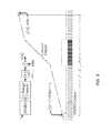
- FIG. 7 is a timing diagram of a preferred embodiment FDC-PLL
- FIG. 8 illustrates a multi-modulus divider applicable to the preferred embodiment FDC-PLLs
- FIG. 9 is a block diagram of a place and route (PNR) digital control logic that provides control logic for the digitally controlled oscillator (DCO) in preferred embodiment FDC-PLLs;
- PNR place and route
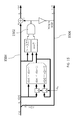
- FIG. 10 is a circuit diagram of a preferred embodiment dual-mode ring oscillator (DMRO);
- FIGS. 11A and 11B are respectively a block diagram and timing diagram of a DMRO preferred embodiment sampling synchronizer
- FIG. 12 is a block diagram of a preferred embodiment binary ripple counter and a wave sampling technique
- FIG. 13 is a DCO block diagram illustrating the preferred embodiment DCO and its control logic
- FIG. 14 shows the simulated phase noise of preferred embodiment FDC-PLLs with and without the DCO's integer boundary avoider circuit enabled
- FIG. 15 illustrates integer boundary avoider circuit logic
- FIG. 16 illustrates an example integer boundary avoider operation
- FIG. 17 is a die photograph of an experimental FDC-PLL in accordance with a preferred embodiment
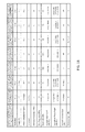
- FIG. 18 compares characteristics and performance of the experimental FDC-PLL to prior PLLs
- FIGS. 19A and 19B are generalized diagrams to that illustrate preferred signal processing of the ⁇ FDC and ring phase calculator of FIG. 1 .
- Preferred embodiment fractional-N phase-locked loop frequency synthesizers based on second-order delta-sigma ( ⁇ ) frequency-to-digital converters (FDCs), referred to as second-order FDC-PLLs, offer advantages of both analog and digital PLL frequency synthesizers in that they have the same quantization noise behavior as analog PLLs based on second-order ⁇ modulators, so like such analog PLLs they can achieve very good spurious tone performance. Yet their loop filters are entirely digital so they are very compact like digital PLLs.
- FIG. 1 shows a preferred embodiment second-order FDC-PLL 100 .
- the input, v ref (t), to the FDC-PLL 100 is a periodic reference signal of frequency f ref
- the output, v out (t), from the FDC-PLL ideally is periodic with frequency (N+ ⁇ )f ref , where N is a positive integer and a is a fractional value in the range ⁇ 1 ⁇ 2 to 1 ⁇ 2.
- the input, v ref (t) is received by a ⁇ frequency-to-digital converter ( ⁇ FDC) 102 and the output is generated from a digitally controlled oscillator (DCO) 104 that is driven by a lowpass digital loop filter (DLF) 106 .
- DCO digitally controlled oscillator
- DLF lowpass digital loop filter
- the ⁇ FDC includes a phase-frequency detector (PFD) 108 and multi-modulus divider 110 of the types used in analog PLLs.
- the PFD generates digital output pulses that goes high when the reference voltage, v ref (t), goes high and go low when the divider output voltage, v div (t), goes high.
- a dual-mode ring oscillator (DMRO) 112 with K (e.g., 13) delay elements is driven by the PFD 108 and its phase is calculated by a digital ring phase calculator 113 .
- a 2 ⁇ z ⁇ 1 digital filter function 114 provides a local feedback path through a divider 120 .
- the DMRO 112 frequency switches from f low to f high when the PFD output, u(t), goes high, and from f high to f low when u(t) goes low, where, in this particular preferred embodiment, f high ⁇ f low ⁇ f PLL .
- each output sample of an accumulator 116 prior to the DLF 106 is nearly proportional to the amount of charge in each charge pump pulse in an analog PLL with second-order ⁇ modulation.
- Its first difference 118 is added to the output of the accumulator 116 prior to the DLF 106 . This has the effect of cancelling most of the quantization noise prior to the DLF, because it replaces e q [n] ⁇ e q [n ⁇ 1] with e Rq [n] ⁇ e Rq [n ⁇ 1].
- preferred specific circuits in accordance with the invention are designed such that ê q [n] is approximately equal to e q [n], so the ⁇ ê q [n] path in the FDC-PLL 100 approximately cancels e q [n] ⁇ e q [n ⁇ 1] prior to the DLF 106 . This allows the PLL bandwidth to be increased without significantly increasing the contribution of quantization noise to the PLL's phase noise.
- the DLF 106 contains a proportional-integral filter which sets the in-band poles and zeros that control the FDC-PLL's dynamics, and it also contains IIR filter stages that introduce four out-of-band poles to further suppress the residual ⁇ quantization noise.
- a linearized model is used to choose the placement of the poles and zeroes.
- a model is provided in Weltin-Wu, C. et al, “A Linearized Model for the Design of Fractional—N Digital PLLs Based on Dual-Mode Ring Oscillator FDCs,” IEEE Transactions on Circuits and Systems, Vol. 62, Issue 8, pages 2013-23 (2015), which is incorporated by reference herein.
- These sampling operations are synchronous with each rising edge of the f ref -rate clock, clk FDC , which is asynchronous with the rising edges of the DMRO inverter outputs.
- Synchronization circuitry is discussed below that enables the sampling to occur without errors and metastability issues. The synchronization circuitry is omitted from FIG. 2 to simplify the ring phase calculator's signal processing explanation.
- the ring phase calculator's 8-bit counter 204 is never reset, so it counts DMRO cycles and rolls over every 256 DMRO cycles. Thus, its output can be viewed as the measured DMRO phase in cycles quantized down to the nearest integer modulo 256.
- the example DMRO 112 includes 13 inverters 202 .
- a phase decoder 206 uses all 13 DMRO inverter outputs to measure the counter's quantization error to a resolution of 1/26 of a DMRO cycle, so its output can be viewed as a quantized version of the counter's quantization error. This is illustrated in FIGS. 3A and 3B , in which the sampling operation prior to the phase decoder is omitted for illustration clarity.
- a clipper 208 shown in FIG. 2 only affects the locking behavior of the PLL because the magnitude of y[n] would be bounded by 2 when the PLL is locked even without the clipper. The purpose of the clipper 208 is to reduce the PLL's worst-case locking time.
- the ring phase calculator 113 subtracts the previous from the current sampled counter output and clears the most significant bit (MSB) of the result.
- MSB most significant bit
- Frequency is the derivative of phase, so it can be verified that these operations result in a measure of the DMRO frequency divided by f ref and quantized to the nearest integer.
- the ring phase calculator 113 subtracts an integer, M, from this frequency measure and accumulates the result to generate y[n].
- M can be set to any integer from 40 to 80). It can be verified that y[n] is the difference between the DMRO's phase in cycles quantized down to the nearest integer and the phase of an ideal oscillator of frequency Mf ref at the time of the nth rising edge of clk FDC .
- the counter increases with a slope that is low when the DMRO frequency is f low and a slope that is higher when the DMRO frequency is f high . Therefore, the counter output is equivalent to the quantized integral of a constant plus the PFD output, u(t), as illustrated in FIG. 4 .
- the ⁇ FDC 102 has local feedback through the divider 120 , because the divider modulus is N ⁇ 2y[n]+y[n ⁇ 1].
- increasing the u(t) pulse width during the nth clk FDC period has the effect of increasing y[n] (as can be seen from the timing diagram in FIG. 4 ), which decreases the divider modulus, which decreases the u(t) pulse width during the (n+1)th clk FDC period.
- FIG. 5A represents the well-known second-order ⁇ modulator.
- the ⁇ FDC equivalence to a ⁇ modulator can be seen from the bottom ⁇ modulator FIG. 5B .
- the 2 ⁇ z ⁇ 1 block of the ⁇ modulator is implemented by the 2 ⁇ z ⁇ 1 block in the ⁇ FDC.
- the second accumulator and quantizer are implemented by the integration and quantization performed by the DMRO and ring phase calculator in the FIG. 1 embodiment.
- the divider's output frequency varies in proportion to both v[n] and the PLL's frequency error, i.e., its deviation from (N+ ⁇ )f ref , so the divider's output phase and, consequently, the width of the u(t) pulse during the nth clk FDC period is proportional to the integral of both v[n] and the PLL's frequency error.
- This integration operation implements the first accumulator in the ⁇ modulator.
- a significant aspect of the above-mentioned ⁇ modulator equivalence is that the ⁇ FDC inherits the self-dithering property of a second-order ⁇ modulator, which suppresses spurious tones that would otherwise occur in its quantization noise.
- GRO gated ring oscillator
- SRO switched ring oscillator
- TDCs time-to-digital converters
- previously-published first-order FDCs that have been used in PLLs are only equivalent to first-order ⁇ modulators, which are notorious for having quantization noise with large spurious tones.
- FIG. 6 shows a diagram of the fabricated FDC-PLL without its test logic or programming interface.
- the only blocks which are fully custom analog are reference generation circuitry connected to the crystal oscillator 602 , the DMRO 112 , and the DCO.
- the custom digital blocks in the IC are comprised entirely of standard cells, but manually laid out. Manual versus automated layout gives better control over parasitics for improved speed and matching.
- the ring phase calculator 113 , the 2 ⁇ z ⁇ 1 function 114 , the DLF 106 , and a portion of the DCO's control logic are all contained in the place and route (PNR) digital.
- FIG. 7 shows a timing diagram for the FIG. 6 IC.
- the ⁇ FDC requires the divider 120 to behave as a non-delaying accumulator, so within one period of clk FDC the u(t) pulse must rise and fall, the DMRO 112 must be sampled, and y[n] and v[n] must be computed, all in time for the divider to be loaded for the next period.
- the DMRO's phase is sampled at the reference frequency, and while it is functionally possible to sample the DMRO on the rising reference edge while u(t) is high and the DMRO frequency is f high , it is much simpler timing-wise to sample on the falling reference edge when u(t) is low and the DMRO's frequency is f low .
- clk FDC is generated from delayed inverted reference edges; the delay and high duty cycle are only used to save power in the synchronizer 604 .
- the ⁇ FDC is not sensitive to jitter on this sampling edge because this noise is added after the second accumulator in the equivalent ⁇ modulator, making it subject to highpass noise shaping just like quantization noise.
- the timing bottleneck in this system is generating v[n] in time to affect the divider's next output edge.
- the value M is preferably chosen (based on f high and f low ) such that the average width of u(t) is 1 ⁇ 4T ref .
- 1 ⁇ 4T ref 34T DCO . It follows from the ⁇ modulator equivalence that y[n] ⁇ 2, so passing y[n] through the 2 ⁇ z ⁇ 1 block ensures
- each u(t) pulse is high for 28 to 40 DCO periods after the rising reference edge.
- u(t) is 28 DCO periods wide, then there are 40 DCO periods between v div (t) and the falling edge of v ref (t). Adding 2 ns for the clk FDC delay, plus a worst case of 2 ns through the synchronizer means the data into the FDC digital is ready no later than 54 DCO periods into the current divider interval.
- FIG. 8 illustrates details of the divider 120 .
- the modulus is split into fixed and variable count intervals such that the modulus for the variable count interval need not be loaded until 8 DCO periods before the end of the prior fixed count interval.
- the divider has a 6-cell 2 ⁇ 3 chain 802 and control logic 804 that re-uses the chain multiple times per division interval.
- div sel 0
- the divider begins each period by dividing by 80.
- the chain is re-loaded with the modulus N ⁇ v[n] ⁇ 80, which completes the division. In this mode the divider can accommodate any modulus from 96 through 133.
- the divider divides by 32 three times for a total of 96, followed by the variable modulus division of N ⁇ v[n] ⁇ 96. In this mode the divider can accommodate any modulus from 134 to 159.
- FDC DIG denotes FDC digital
- DCO DIG denotes DCO digital
- Its clock, clk fast is generated by the divider's 3 rd 2 ⁇ 3-stage output, which has an average frequency of f dco /8.
- the FDC digital, DLF 106 , and a portion of the DCO digital are all clocked at the reference rate by gated versions of clk fast .
- the synchronizer generates the signal rdy which indicates that the sampled DMRO outputs and the ring phase calculator's sampled counter output are valid.
- the rdy signal is retimed in the PNR digital because it is asynchronous with respect to clk fast . This introduces a delay of 0.5-1.5 clk fast periods.
- the output of the FDC digital is ready one clk fast period after that, for a total of 1.5-2.5 clk fast or 12-20 clk DCO periods between synchronizer data to v[n] output. In total, the v[n] output is ready by the 65 th -74 th DCO period, well before the 88 th period when the divider is loaded.
- the rdy signal continues to propagate down the register chain, gating the clock to the DLF and slow (i.e. f ref -rate) portion of the DCO digital.
- This sequence completes before the next reference edge so that when u(t) goes high, the majority of the PNR digital has completed switching. This results in a quiet environment for the DMRO, whose supply sensitivity was measured to be ten times higher when its frequency is f high than when its frequency is f low .
- the DLF's output, d[n], is synchronous with clk fast , so upsampling it within the DCO digital does not require resynchronization.
- the DCO digital outputs are retimed by a set of flip-flops near the DCO's FCE elements that are powered by the DCO's supply. These flip-flops are clocked by a version of clk fast that is passed directly from the divider to the DCO to minimize jitter.
- DMRO tuning is achieved by current starving the oscillator core.
- the DMRO's low frequency, f low is tunable from 0.4-3.4 GHz by two SPI-controllable 4-bit resistor arrays, one between VDD and the core, and the other between the core and ground.
- Its high frequency, f high is controlled in the same way, except transistors in triode are used in place of resistors.
- Four-bit tuning gives an f high range of 1.8-5.1 GHz.
- the u(t) signal is buffered and drives switches that connect the MOS array to the core, bypassing the resistor array, so as to modulate the DMRO between f low and f high .
- a well-known property of charge-pump based analog PLLs is their low sensitivity to non-ideal charge pump switching transients provided that the charge pump current is allowed to fully settle between transient events, and that the rising and falling transient shapes are independent of when the current sources are turned on or off, respectively.
- non-ideal DMRO transients between f high and f low do not degrade the FDC-PLL's performance provided the DMRO frequency is allowed to fully settle before u(t) transitions or the DMRO is sampled, and that the rising and falling frequency transient shapes are independent of the times of the rising and falling edges of u(t), respectively.
- FIGS. 11A and 11B respectively show the circuit and timing diagrams of the synchronizer 602 .
- the synchronizer solves two problems which arise from asynchronous sampling of the DMRO by clk FDC . The first is that inevitable timing skew between the counter sampler and DMRO sampler will cause glitches near counter increments because the counter will not increment at the exact moment the DMRO phase wraps. The second is that even if the two paths are aligned, if the binary counter is sampled while it is incrementing, hugely incorrect sampled values may result.
- the samp frac signal is a buffered version of clk FDC that samples the DMRO's phases p 0 (t), p 1 (t), . . . , p 12 (t) to produce s 0 [n], . . . , s 12 [n].
- p 1 (t) p 1 (t)
- p 12 (t) outputs transitions at a time, and incorrect samples of the actively transitioning output result in a decoded phase that is one 1/26th of a period (one fractional quantization step) in error.
- the pair of DMRO phases p 0 (t) and p 6 (t) are roughly in quadrature, so the pair of samples (s 0 [n], s 6 [n]) determine in which of roughly four equal parts of a clk DMRO period the samp frac rising edge occurs.
- Two delay lines clocked on clk DMRO sample clk FDC , one starting with a rising edge and the other with the falling edge. Based on which of the four clk DMRO period sub-intervals the samp frac rising edge has arrived, the delay line which sampled clk FDC furthest from its rising edge is selected.
- the delay lines lengths are such that the generated samp int edge is always 1.5 clk DMRO periods after the clk DMRO period in which the samp frac rising edge arrived, allowing the samples s 0 [n] and s 6 [n] to settle before the MUX decision is required; this adds a constant offset to c[n], which is irrelevant because c[n] is first differenced in the ring phase calculator.
- the synchronizer is not sensitive to timing skew between clk DMRO and clk FDC up to a quarter of a clk DMRO period, T DMRO . For example, if samp frac is delayed relative to clk FDC , then if clk FDC lands in the later part of the (0,1) interval, the samples (s 0 [n],s 6 [n]) may be (0,0) rather than (1,0).
- sampling first with the falling edge rather than the rising edge still gives the correct result, because if the timing skew is less than one quarter of a DMRO period there are no falling clk DMRO edges between clk FDC and samp frac .
- 1 ⁇ 4T DMRO delay matching is easy to achieve.
- FIG. 12 shows how the binary ripple counter is “wave” sampled sequentially wherein the propagation speed of the wave is designed to approximately equal the propagation speed of the ripple down the counter bits. This reduces the effective propagation delay of the counter to the difference between the total ripple delay and the total wave delay, which can be made quite small by again using matched paths and replica delays in layout.
- FIG. 13 shows the LC-based DCO, which passes the DLF's 14-bit output d[n] through the integer boundary avoider—explained below—which essentially generates c I [n] from the 6 MSBs of d[n] (integer part) and x F [n] from the 8 LSBs of d[n] (fractional part).
- the integer part is encoded to drive the slow frequency control element (FCE) bank, a 2-2-2 . . . 2-1 segmented array of 63 FCEs updated at the reference rate.
- the FCE creates a capacitance step of 32 aF which is equivalent to a 27 kHz frequency step at 3.5 GHz, giving the slow FCE bank 1.7 MHz of tuning range.
- the fractional part is upsampled by clk df and requantized by a 2 nd -order digital ⁇ modulator into a 5-level sequence.
- This sequence is DEM-randomized to produce dcw F [n], which drives a fast FCE bank comprised of four FCEs.
- In parallel with the slow and fast FCE banks is a binary-weighted capacitor array controlled via the SPI interface that has 12 bits of tuning spanning 2.8-3.5 GHz, with a 400 kHz step size at 3.5 GHz.
- the main inductor is a custom 2-turn 1 nH center-tapped coil, and the regeneration is provided by a cross-coupled thick-oxide NMOS pair with a tail resonant tank and triode-MOS tail source.
- the inductors, capacitors, and all metal routing were designed and extracted using the EMX 3D field solver.
- the invention includes an integer boundary avoider.
- the integer boundary avoider technique presented in FIG. 15 can be applied to any digital PLL that contains a digitally controlled oscillator (DCO), including the preferred embodiment of FIG. 1 , but not limited to the present FDC-PLL.
- DCO digitally controlled oscillator
- the wrapping of x F [n] will impart a frequency change equal to the average frequency step of the four FCEs in the fast bank.
- the increment or decrement of the slow bank will impart a frequency change equal to the frequency step of the particular slow element that is switched. Because the LSB resolution of d[n] is 105 Hz, the FCEs in the slow bank must match the average of the FCEs in the fast bank to better than 105 Hz, which is 2 8 times smaller than the FCE's 27 kHz frequency step. Achieving 8 bits of matching from 32 aF capacitors is impossible, so in practice large frequency glitches are injected each time an integer boundary is crossed.
- FIG. 14 shows a simulation of the FDC-PLL that demonstrates the effect it can have on phase noise.
- the integer boundary avoider in FIG. 15 mitigates this problem by minimizing the change of c I [n] so as to reduce the number of physical integer boundary crossings.
- an AND gate 1502 output When an AND gate 1502 output is high, it subtracts one from an integer path 1504 , and when it is low, it subtracts 2 8 from a fractional path 1506 ; thus the sum c F [n]+2 ⁇ 8 x F [n] always equals d[n] ⁇ 1.
- FIG. 17 is an image of a prototype IC of the invention.
- the separation portions are labelled with the divisions shown in FIG. 6 , which include the four separate power domains on the die: reference, FDC, digital, and DCO.
- the IC has one global ground provided by a low-impedance metal mesh that covers the active layout wherever possible. The use of a single ground simplified block-to-block communication as all signals were passed differentially with a ground shield, minimizing inter-supply current.
- the prototype provided a 3.5 GHz digital fractional-N PLL in 65 nm CMOS technology that achieves phase noise and spurious tone performance comparable to those of a high-performance analog PLL.
- the PLL's largest in-band fractional spur is ⁇ 60 dBc
- its worst-case reference spur is ⁇ 81 dBc
- its phase noise is ⁇ 93, ⁇ 126, and ⁇ 151 dBc/Hz at offsets of 100 kHz, 1 MHz, and 20 MHz, respectively.
- Its active area is 0.34 mm 2 and it dissipates 15.6 mW from a 1 V supply.
- Each supply is heavily filtered with passive RC networks occupying any unused layout area, and the FDC supply was further sub-divided into four additional RC-filtered domains: PFD, divider, DMRO, and all the DMRO sampling/synchronization logic.
- the RC-filter bandwidths were insufficiently low to have an appreciable impact on the fundamental harmonics of their supply currents.
- they were highly effective at minimizing supply bounces due to bondwire ringing from impulsive currents, which would have otherwise coupled back into its own circuitry or inductively to nearby bondwires.
- the prototype IC contains the FDC-PLL in FIG. 6 as well as analog and digital test circuitry to measure internal voltages, clocks, and register values.
- the SPI interface logic and programming registers occupy 20% of the PNR digital area.
- the IC was fabricated in ST 65 nm single poly, 7 copper CMOS process, and makes use of the dual oxide (LP and GP transistors both available) as well as high-resistivity poly process options.
- the die which measures 1.0 ⁇ 1.3 mm 2 is shown in FIG. 17 .
- the active area which includes inductor density transition regions and all on-chip decoupling capacitance, is 0.34 mm 2
- the area breakdown is given in Table 1.
- the IC is packaged in a QFN32 package with a ground paddle. Sixteen copies of the IC were tested with a compression socket, of which 4 were damaged by a software bug that caused the IC to briefly receive 5 V during startup. Comprehensive measurements taken on the remaining 12 copies were all consistent. The presented spurious results were measured from one part because it was discovered that soldering the IC to the test board improves its spurious performance by 2-3 dB. This was determined by comparing the before-and-after-soldering measurement data for this particular part. The QFN footprint on the board was tinned rather than leveled and gold plated. It is suspected that unevenness in the tinning caused one or more pads to make poor contact when using the socket, which is corroborated by the fact that over-spec clamp-down pressure was required before the IC even drew current from the supply.
- the test board contains an Abracon ABM8G 26 MHz crystal for the XO and a TDK HHM1583B1 wideband RF balun to match the differential output buffer to the measurement equipment.
- Power to the four supply domains is provided by Analog Devices ADP171 voltage regulators with parallel 10 uF X5R and 100 pF NP0 ceramic capacitors. While having independent supplies enabled characterization of individual blocks, for the measurements presented (with the exception of the DCO open loop measurement discussed below) all the IC supply domains were connected together and driven with one regulator.
- the test board was connected to a motherboard that supplied power and USB communication to the measurement PC.
- phase noise measurements were taken with an Agilent E5052B signal source analyzer, and the spurious tone measurements were taken with an Agilent N9020A spectrum analyzer.
- all measurements, data collection, screen captures and plot generation were performed using an automated suite of Python scripts.
- the FDC-PLL's phase noise for a 3.5 GHz output with a 400 Hz fractional frequency offset is shown in FIG. 18 .
- the PLL exceeds GSM phase noise requirements which remain among the most difficult specifications to meet.
- the phase noise contributions of all the individual blocks were extrapolated to produce the plot shown in FIG. 18 .
- an output-power-limiting impedance mismatch limits the phase noise floor, as 20 MHz spot phase noise as low as ⁇ 154 dBc/Hz has been observed in the lab with a high-quality SMA cable.
- the same generic SMA cable was used for all measurements.
- the DCO's true low frequency noise was only visible after a 220 ⁇ F electrolytic capacitor was added in parallel with those already attached to the DCO supply regulator.
- the PLL had sufficiently wide bandwidth to suppress the DCO regulator noise, making the electrolytic capacitor unnecessary.
- the reference spur measured was ⁇ 81 dBc. Due to the asymmetry of the negative and positive offset spurs, it is suspected that the origin of the ⁇ 81 dBc spur is direct coupling, e.g. through bondwires, not upconversion within the PLL. Repeated sweeps of the spectrum analyzer showed the positive offset spur sometimes disappearing below the noise floor, while the ⁇ 81 dBc negative-side reference spur remained constant. It is therefore a worst-case bound on reference spur performance. Spectrum analyzer averaging was disabled for this and all spur measurements.
- the PLL's fractional frequency offset ⁇ was swept from 0 to 1 ⁇ 2 and the PLL's worst fractional spur for each value of ⁇ was determined.
- the spectrum analyzer's span, sweep time and resolution bandwidth were automatically adjusted for each value of ⁇ to ensure the noise floor was low enough to see spurs, and that 5 negative and positive harmonics of ⁇ f ref were always visible.
- the worst fractional spur was always either the first or second, and neither exceeded ⁇ 60 dBc.
- the FDC-PLL's measured performance is summarized in FIG. 18 along with that of the best comparable PLLs published to date. As indicated, the FDC-PLL has excellent phase noise performance with the lowest supply voltage, lowest power dissipation, and best spurious tone performance in its class. Compared to other PLLs with similarly low phase noise, the FDC-PLL achieves an order of magnitude lower spurious tone power than previously reported.
- the comparisons in FIG. 18 are to:
- FIGS. 19A and 19B respectively show generalized versions of the FIG. 1 ⁇ FDC102 and the FIG. 2 ring phase calculator 113 .
- FIGS. 19A and 19B are labelled with variables that can be used for more generalized designs consistent with the preferred embodiments. The following considerations can aid such designs and provide details about additional preferred embodiments.
- An analysis of the performance of the FIGS. 19A and 19B embodiment with effects of non-ideal circuit behavior is included in Weltin-Wu, C. et al, “A Linearized Model for the Design of Fractional—N Digital PLLs Based on Dual-Mode Ring Oscillator FDCs,” IEEE Transactions on Circuits and Systems, Vol. 62, Issue 8, pages 2013-23 (2015), which is incorporated by reference herein.
- the DMRO 112 is preferably implemented as a ring of K nominally identical inverters (delay elements). Each inverter has a propagation delay that is one of two values depending on whether the top PFD 108 output, u(t), is high or low.
- the nominal instantaneous output frequency of the DMRO (neglecting switching transients) is given by:
- u(t) is the top PFD output
- f high and f low are constants.
- T ref 1/f ref is the reference period
- J is an integer chosen under the constraint that 2 1-J K must be integer-valued
- M is a positive integer
- T ⁇ must satisfy
- T ⁇ is the average PFD 108 pulse width, and the DMRO 112 is locked to an average frequency of Mf ref .
- the integer J is a design parameter that specifies a tradeoff between the DMRO's frequency spread and its contribution to the FDC-PLL's overall phase noise. It is not critical that (2) and (3) be satisfied exactly or that the frequency transitions are instantaneous.
- the input to the ring phase calculator 114 is the DMRO's set of K inverter outputs.
- the C-bit counter is clocked by one of the DMRO inverter outputs, so the counter increments once per DMRO cycle and rolls over modulo 2 C .
- the C counter bits are interpreted as an unsigned number in the range ⁇ 0, 1, 2, . . . , 2 C ⁇ 1 ⁇ .
- the ring phase calculator's clock signal, clk FDC is an inverted version of the reference, so its period is T ref .
- the number of counter bits is chosen to satisfy:
- the C-bit counter output represents the integer part of the DMRO's phase modulo 2 C . Therefore, the fractional part of the phase goes to zero each time the counter output increments or rolls over.
- p R [n] in FIG. 19B is the sum of the sampled counter output and the fractional phase decoder output. It is interpreted as an unsigned fixed-point sequence with the C sampled counter bits forming its integer part and the F fractional phase decoder bits forming its fractional part.
- p R [n] is a quantized representation of the absolute DMRO phase in cycles measured at the nth rising edge of clk FDC that rolls over modulo 2 C cycles.
- the portion of the ring phase calculator to the right of p R [n] performs two's complement arithmetic.
- the sequence f R [n] is obtained by performing a two's complement difference of p R [n] and p R [n ⁇ 1], and replacing the MSB with zero.
- the ring phase calculator output, y[n] is an integer-valued two's complement sequence formed from the 3 MSBs of r[n].
- the ⁇ ê q [n] output is a fractional two's complement sequence formed from the F ⁇ J LSBs of r[n] with an appended MSB set to 0.
- the most troublesome non-ideal fractional-N PLL behavior is the generation of fractional spurious tones in the PLL's output.
- All fractional-N PLLs perform quantization, which is a highly nonlinear operation, so this is a potential source of fractional spurious tones.
- the self-dithering property of higher-than-first-order, multi-bit ⁇ modulation ideally suppresses spurious tones.
- Non-ideal circuit behavior can degrade the ⁇ FDC's equivalence to a second-order ⁇ modulator, which can degrade the self-dithering property. This can be addressed by designs that ensure that the DMRO has time to settle each time it changes frequency.
Landscapes
- Engineering & Computer Science (AREA)
- Computer Networks & Wireless Communication (AREA)
- Signal Processing (AREA)
- Stabilization Of Oscillater, Synchronisation, Frequency Synthesizers (AREA)
Abstract
Description
| TABLE 1 | |||
| Total active area (mm2) | 0.34 | ||
| PNR digital | 0.07 | ||
| XO and reference buffers | 0.005 | ||
| DCO and output buffer | 0.21 | ||
| ΔΣ FDC | 0.02 | ||
| Decoupling capacitance | 0.035 | ||
- A—R. B. Staszewski, J. Wallberg, S. Rezeq, C.-M. Hung, O. Eliezer, S. Vemulapalli, C. Fernando, K. Maggio, R. Staszewski, N. Barton, M.-C. Lee, P. Cruise, M. Entezari, K. Muhammad, D. Leipold, “All-Digital PLL and Transmitter for Mobile Phones,” IEEE Journal of Solid-State Circuits, vol. 40, no. 12, pp. 2469-2482, December, 2005.
- B—H. H. Chang, P-Y. Wang, J.-H. C. Zhan, H. Bing-Yu, “A Fractional Spur-Free ADPLL with Loop-Gain Calibration and Phase-Noise Cancellation for GSM/GPRS/EDGE,” IEEE International Solid-State Circuits Conference, pp. 200-201, 606, February 2008.
- C—E. Temporiti, C. Weltin-Wu, D. Baldi, M. Cusmai, and F. Svelto, “A 3.5 GHz Wideband ADPLL With Fractional Spur Suppression Through TDC Dithering and Feedforward Compensation,” IEEE Journal of Solid-State Circuits, vol. 45, no. 12, pp. 2723-2736, December 2010.
- D—L. Vercesi, L. Fanori, F. De Bernardinis, A. Liscidini, and R. Castello, “A Dither-Less All Digital PLL for Cellular Transmitters,” IEEE Journal of Solid-State Circuits, vol. 47, no. 8, pp. 1908-1920, August 2012.
- E—K. Takinami, R. Strandberg, P. C. P. Liang, G. L. G. de Mercey, T. Wong, M. Hassibi, “A rotary-traveling-wave-oscillator-based all-digital PLL with a 32-phase embedded phase-to-digital converter in 65 nm CMOS,” IEEE International Solid-State Circuits Conference, pp. 100-102, February 2011.
- F—Hsu, M. Z. Straayer, M. H. Perrott, “A Low-Noise, Wide-BW 3.6 GHz Digital ΔΣ Fractional-N Frequency Synthesizer with a Noise-Shaping Time-to-Digital Converter and Quantization Noise Cancellation,” IEEE International Solid-State Circuits Conference, pp. 340-341, February 2008.
r[n]=r[n−1]+2J(f R [n]−M) (8)
Claims (14)
Priority Applications (1)
| Application Number | Priority Date | Filing Date | Title |
|---|---|---|---|
| US15/052,578 US10158366B2 (en) | 2016-02-24 | 2016-02-24 | Digital fractional-N PLL based upon ring oscillator delta-sigma frequency conversion |
Applications Claiming Priority (1)
| Application Number | Priority Date | Filing Date | Title |
|---|---|---|---|
| US15/052,578 US10158366B2 (en) | 2016-02-24 | 2016-02-24 | Digital fractional-N PLL based upon ring oscillator delta-sigma frequency conversion |
Publications (2)
| Publication Number | Publication Date |
|---|---|
| US20170244544A1 US20170244544A1 (en) | 2017-08-24 |
| US10158366B2 true US10158366B2 (en) | 2018-12-18 |
Family
ID=59629548
Family Applications (1)
| Application Number | Title | Priority Date | Filing Date |
|---|---|---|---|
| US15/052,578 Active US10158366B2 (en) | 2016-02-24 | 2016-02-24 | Digital fractional-N PLL based upon ring oscillator delta-sigma frequency conversion |
Country Status (1)
| Country | Link |
|---|---|
| US (1) | US10158366B2 (en) |
Cited By (8)
| Publication number | Priority date | Publication date | Assignee | Title |
|---|---|---|---|---|
| US10897259B1 (en) | 2019-07-11 | 2021-01-19 | Samsung Electronics Co., Ltd. | Phase locked circuit, method of operating the same, and transceiver |
| US20220321132A1 (en) * | 2021-03-23 | 2022-10-06 | Nxp B.V. | Type-i plls for phase-controlled applications |
| US11569831B1 (en) * | 2022-03-23 | 2023-01-31 | Infineon Technologies Ag | Time-to-digital converter calibration |
| US20230126891A1 (en) * | 2021-10-27 | 2023-04-27 | Nxp B.V. | Circuitry and methods for fractional division of high-frequency clock signals |
| US20240030932A1 (en) * | 2022-07-20 | 2024-01-25 | Ciena Corporation | Apparatus and method for sigma-delta modulator quantization noise cancellation |
| US20240205059A1 (en) * | 2022-12-16 | 2024-06-20 | Commissariat A L'energie Atomique Et Aux Energies Alternatives | System for generating at least one radio frequency signal phase-locked to a reference signal, corresponding radio frequency transmitter and receiver |
| US12231136B2 (en) | 2021-03-23 | 2025-02-18 | Nxp B.V. | Type-I PLLs for phase-controlled applications |
| US12603655B1 (en) * | 2024-04-02 | 2026-04-14 | Cadence Design Systems, Inc. | Subranging digital to time converter-based fractional phase locked loop architecture |
Families Citing this family (10)
| Publication number | Priority date | Publication date | Assignee | Title |
|---|---|---|---|---|
| US10009036B2 (en) * | 2016-09-09 | 2018-06-26 | Samsung Electronics Co., Ltd | System and method of calibrating input signal to successive approximation register (SAR) analog-to-digital converter (ADC) in ADC-assisted time-to-digital converter (TDC) |
| US10050634B1 (en) * | 2017-02-10 | 2018-08-14 | Apple Inc. | Quantization noise cancellation for fractional-N phased-locked loop |
| US11079723B2 (en) | 2018-02-06 | 2021-08-03 | Integrated Device Technology, Inc. | Apparatus and methods for automatic time measurements |
| US10707879B2 (en) * | 2018-04-13 | 2020-07-07 | KaiKuTek Inc. | Frequency-modulated continuous-wave radar system and frequency tracking method for calibrating frequency gains of a radio frequency signal to approach wideband flatness frequency responses |
| US10826514B1 (en) | 2019-10-15 | 2020-11-03 | Ciena Corporation | Noise-shaping enhanced gated ring oscillator based analog-to-digital converters |
| IL275511B2 (en) | 2020-06-18 | 2023-11-01 | Capow Tech Ltd | High-accuracy adaptive digital frequency synthesizer for wireless power systems |
| KR102962955B1 (en) * | 2020-09-21 | 2026-05-08 | 삼성전자주식회사 | Apparatuse for phase locking loop and method of operating the phase locking loop |
| US11533058B2 (en) * | 2020-12-17 | 2022-12-20 | Qualcomm Incorporated | Digital phase-frequency detector with split control loops for low jitter and fast locking |
| US20250202510A1 (en) * | 2021-09-17 | 2025-06-19 | Point2 Technology, Inc. | 50 gb/s pam4 bi-directional plastic waveguide link having carrier synchronization using pi-based costas loop |
| US12603657B2 (en) * | 2024-04-12 | 2026-04-14 | Shaoxing Yuanfang Semiconductor Co., Ltd. | Reducing non-linearity in a digital-to-time converter (DTC) due to unequal successive input codes specifying respective delays |
Citations (9)
| Publication number | Priority date | Publication date | Assignee | Title |
|---|---|---|---|---|
| US20100141314A1 (en) * | 2008-12-09 | 2010-06-10 | Sunplus Technology Co., Ltd. | All digital phase locked loop circuit |
| US7888973B1 (en) * | 2007-06-05 | 2011-02-15 | Marvell International Ltd. | Matrix time-to-digital conversion frequency synthesizer |
| US20110133799A1 (en) * | 2009-12-07 | 2011-06-09 | Qualcomm Incorporated | Configurable digital-analog phase locked loop |
| US20120194369A1 (en) * | 2011-01-28 | 2012-08-02 | The Regents Of The University Of California | Ring oscillator delta sigma adc modulator with replica path nonlinearity calibration |
| US20140368366A1 (en) * | 2013-06-12 | 2014-12-18 | The Regents Of The University Of California | Mostly-digital open-loop ring oscillator delta-sigma adc and methods for conversion |
| US20150145567A1 (en) * | 2013-11-27 | 2015-05-28 | Silicon Laboratories Inc. | Cancellation of spurious tones within a phase-locked loop with a time-to-digital converter |
| US20160065224A1 (en) * | 2014-08-27 | 2016-03-03 | Qualcomm Incorporated | Fast frequency throttling and re-locking technique for phase-locked loops |
| US20160233870A1 (en) * | 2013-09-16 | 2016-08-11 | Entropic Communications, Llc | Digitally controlled oscillator |
| US20170214408A1 (en) * | 2014-08-01 | 2017-07-27 | Mediatek Inc. | Switched-capacitor loop filter |
-
2016
- 2016-02-24 US US15/052,578 patent/US10158366B2/en active Active
Patent Citations (9)
| Publication number | Priority date | Publication date | Assignee | Title |
|---|---|---|---|---|
| US7888973B1 (en) * | 2007-06-05 | 2011-02-15 | Marvell International Ltd. | Matrix time-to-digital conversion frequency synthesizer |
| US20100141314A1 (en) * | 2008-12-09 | 2010-06-10 | Sunplus Technology Co., Ltd. | All digital phase locked loop circuit |
| US20110133799A1 (en) * | 2009-12-07 | 2011-06-09 | Qualcomm Incorporated | Configurable digital-analog phase locked loop |
| US20120194369A1 (en) * | 2011-01-28 | 2012-08-02 | The Regents Of The University Of California | Ring oscillator delta sigma adc modulator with replica path nonlinearity calibration |
| US20140368366A1 (en) * | 2013-06-12 | 2014-12-18 | The Regents Of The University Of California | Mostly-digital open-loop ring oscillator delta-sigma adc and methods for conversion |
| US20160233870A1 (en) * | 2013-09-16 | 2016-08-11 | Entropic Communications, Llc | Digitally controlled oscillator |
| US20150145567A1 (en) * | 2013-11-27 | 2015-05-28 | Silicon Laboratories Inc. | Cancellation of spurious tones within a phase-locked loop with a time-to-digital converter |
| US20170214408A1 (en) * | 2014-08-01 | 2017-07-27 | Mediatek Inc. | Switched-capacitor loop filter |
| US20160065224A1 (en) * | 2014-08-27 | 2016-03-03 | Qualcomm Incorporated | Fast frequency throttling and re-locking technique for phase-locked loops |
Non-Patent Citations (44)
| Title |
|---|
| Amr Elshazly, SachinRao, Brian Young, Member and Pavan Kumar Hanumolu, "A Noise-Shaping Time-to-Digital Converter Using Switched-Ring Oscillators-Analysis, Design, and Measurement Techniques", Oregon State University, Qualcomm, Marvell Semiconductor, University of Illinois, IEEE Journal of Solid-State Circuits, vol. 49, No. 5, May 2014. * |
| Bax, W.T., et al., "A GMSK Modulator Using a ΔΣ Frequency Discriminator-Based Synthesizer", IEEE Journal of Solid-State Circuits, vol. 36, No. 8, (Aug. 2001), pp. 1218-1227. |
| Borremans, J., et al., "A 86MHz-to-12GHz Digital-Intensive Phase-Modulated PLL for Software-Defined Radi19os, Using a 6fJ/Step TDC in 40nm digital CMOS", IEEE Journal of Solid-State Circuits, vol. 45, No. 10, (Oct. 2010), pp. 2116-2129. |
| Chang, H. H., et al, "A Fractional Spur-Free ADPLL with Loop-Gain Calibration and Phase-Noise Cancellation for GSM/GPRS/EDGE", IEEE International Solid-State Circuits Conference, vol. 606, (Feb. 2008), pp. 200-201. |
| Chen, J., et al., "The design of all-digital polar transmitter based on ADPLL and phase synchronized ΔΣ modulator", IEEE Journal of Solid-State Circuits, vol. 47, No. 5, (May 2012), pp. 1154-1164. |
| Chen, M.S., et al., "A Calibration-Free 800 MHz Fractional-N Digital PLL With Embedded TDC", IEEE Journal of Solid-State Circuits, vol. 45, No. 12, (Dec. 2010), pp. 2819-2827. |
| Christian Venerus and Ian Galton, "A TDC-Free Mostly-Digital FDC-PLL Frequency Synthesizer With a 2.8-3.5 GHz DCO", Qualcomm Technologies and University of California, IEEE, Nov. 10, 2014. * |
| Christian Venerus and Ian Galton, Delta-Sigma FDC Based Fractional-PLLs, Univeristy of California at San Diego, IEEE, 2012. * |
| Chun-Ming Hsu, Matthew Z. Straayer, and Michael H. Perrott, A Low-Noise Wide-BW 3.6-GHz Digital delta sigma Fractional-N Frequency Synthesizer With a Noise-Shaping Time-to-Digital Converter and Quantization Noise Cancellation, IEEE Journal of Solid-State Circuits, vol. 43, No. 12, Dec. 2008. * |
| Colin Weltin-Wu, Eythan Familier, Ian Galton,"A Linearized Model for the Design of Fractional-Digital PLLs Based on Dual-Mode Ring Oscillator FDCs", University of California, Aug. 2015. * |
| Colin Weltin-Wu, Guobi Zhao, Ian Galton, "A Highly-Digital Frequency Synthesizer Using Ring-Oscillator Frequency-to-Digital Conversion and Noise Cancellation", Analog Devices, University of California, Feb. 25, 2015. * |
| Colin Weltin-Wu, Guobi Zhao, Ian Galton,"A 3.5 GHz Digital Fractional-N PLL Frequency Synthesizer Based on Ring Oscillator Frequency-to-Digital Conversion", Analog Devices, Spreadtrum, University of California, Nov. 24, 2015. * |
| De Muer, B., et al., "A CMOS monolithic ΔΣ-controlled fractional-N frequency synthesizer for DCS-1800", IEEE Journal of Solid-State Circuits, vol. 37, No. 7, (Jul. 2002), pp. 835-844. |
| Galton, Ian, "Granular Quantization Noise in a Class of Delta-Sigma Modulators", IEEE Transactions on Information Theory, vol. 40, No. 3, (May 1994), pp. 848-859. |
| Hedayati, H., et al., "A 1 MHz Bandwidth, 6 GHz 0.18 μm CMOS Type-I ΔΣ Fractional-N Synthesizer for WiMAX Applications", IEEE Journal of Solid-State Circuits, vol. 44, No. 12, (Dec. 2009), pp. 3244-3252. |
| Ian Galton, "Delta-Sigma Fractional-N Phase-Locked Loops", RF microelectronics, Razavi, B. (Editor), Prentice Hall, 1998. |
| Jee, D.-W., "A 2GHz fractional-N digital PLL with 1b noise shaping TDC", IEEE Journal of Solid-State Circuits, vol. 47, No. 4, (Apr. 2012), pp. 875-883. |
| Kratyuk, V., et al., "A Digital PLL With a Stochastic Time-to-Digital Converter," IEEE Transactions on Circuits and Systems I: Regular Papers, vol. 56, No. 8, (Aug. 2009), pp. 1612-1621. |
| Lee, M., et al., "A low-noise wideband digital phase-locked loop based on a coarse-fine time-to-digital converter with subpicosecond resolution", IEEE Journal of Solid-State Circuits, vol. 44, No. 10, (Oct. 2009), pp. 2808-2816. |
| Levantino, S., et al., "An Adaptive Pre-Distortion Technique to Mitigate the DTC Nonlinearity in Digital PLLs", IEEE Journal of Solid-State Circuits, to appear, vol. 49, No. 8, (Aug. 2014), pp. 1762-1772. |
| Li, L., et al., "A 5.8GHz Digital Arbitrary Phase-setting Type II PLL in 65nm CMOS with 2.25o Resolution", IEEE Asian Solid-State Circuits Conference, (Nov. 2012), pp. 317-320. |
| M. Talegaonkar, T. Anand, A. Elkholy, A. Elshazly, R. K. Nandwana, S. Saxena, B. Young, W. Choi, P. K. Hanumolu, A 4.4-5.4GHz Digital Fractional-N PLL Using ΔΣ Frequency-to-Digital Converter, 2014 Symposium on VLSI Circuits Digest of Technical Papers. * |
| Marzin, G., "A 20Mb/s Phase Modulator Based on a 3.6GHz Digital PLL with -36dB EVM at 5mW Power", IEEE International Solid-State Circuits Conference, vol. 47, No. 12, (Dec. 2012), pp. 342-343. |
| Miller, B., et al., "A multiple modulator fractional divider", Annual IEEE Symposium on Frequency Control, vol. 44, (Mar. 1990), pp. 559-568. |
| Park, C., et al., "A 1.8-GHz self-calibrated phase-locked loop with precise I/Q matching", IEEE Journal of Solid-State circuits, vol. 36, No. 5, (May 2001), pp. 777-783. |
| Schreier, R., et al., "Understanding Delta-Sigma Data Converters", John Wiley and Sons, (2005). |
| Shen, B., et al., "An 8.5 mW, 0.07 mm2 ADPLL in 28 nm CMOS with Sub-ps Resolution TDC and < 230 fs RMS Jitter", Symposium on VLSI Circuits, (Jun. 2013), pp. C192-C193. |
| Staszewski, R.B., et al., "All-Digital PLL and GSM/EDGE Transmitter in 90nm CMOS", IEEE International Solid-State Circuits Conference, (Feb. 2005), pp. 316-317. |
| Takinami, K, et al., "A rotary-traveling-wave-oscillator-based all-digital PLL with a 32-phase embedded phase-todigital converter in 65nm CMOS", IEEE International Solid-State Circuits Conference, (Feb. 2011), pp. 100-102. |
| Tasca, D., et al., "A 2.94-to-4.0 GHz fractional-N digital PLL with bang-bang phase detector and 560 fs rms integrated jitter at 4.5 mW power", IEEE Journal of Solid-State Circuits, vol. 46, No. 12, (Dec. 2011), pp. 2745-2758. |
| Temporiti, E., et al., "A 3.5 GHz Wideband ADPLL With Fractional Spur Suppression Through TDC Dithering and Feedforward Compensation", IEEE Journal of Solid-State Circuits, vol. 45, No. 12, (Dec. 2010), pp. 2723-2736. |
| Temporiti, E., et al., "A 700 kHz Bandwidth ΔΣ Fractional Synthesizer with Spurs Compensation and Linearization Techniques for WCDMA Applications", IEEE Journal of Solid-State Circuits, vol. 39, No. 9, (Sep. 2004), pp. 1446-1454. |
| Tokairin, T., et al., "A 2.1-to-2.8-GHz low-phase-noise all-digital frequency synthesizer with a time-windowed time-to-digital converter," IEEE Journal of Solid-State Circuits, vol. 45, No. 12, (Dec. 2010), pp. 2582-2590. |
| Tonietto, R., et al., "A 3 MHz Bandwidth Low Noise RF All Digital PLL with 12ps Resolution Time-to-Digital Converter," European Solid-State Circuits Conference, (Sep. 2006), pp. 150-153. |
| Ueda, K., et al., "A Digital PLL with Two-step Closed-locking for Multi-mode/Multi-band SAW-less Transmitter", IEEE Custom Integrated Circuits Conference, (Sep. 2012), pp. 1-4. |
| Vaucher, C.S., et al., "A family of low-power truly modular programmable dividers in standard 0.35-um CMOS technology", IEEE Journal of Solid-State Circuits, vol. 35, No. 7, (Jul. 2000), pp. 1039-1045. |
| Venerus, C., et al., "Delta-Sigma FDC Based Fractional-N PLLs", IEEE Transactions on Circuits and Systems I: Regular Papers, vol. 60, No. 5, (May 2013), pp. 1274-1285. |
| Vercesi, L., et al., "A Dither-Less All Digital PLL for Cellular Transmitters", IEEE Journal of Solid-State Circuits, vol. 47, No. 8, (Aug. 2012), pp. 1908-1920. |
| Waheed, K., et al., "Spurious free time-to-digital conversion in an ADPLL using short dithering sequences", IEEE Custom Integrated Circuits Conference, (Sep. 2010), pp. 1-4. |
| Weltin-Wu, C., et al., "A 3 GHz Fractional-N All-Digital PLL with Precise Time-to-Digital Converter Calibration and Mismatch Correction", IEEE International Solid-State Circuits Conference, (Feb. 2008), pp. 344-345. |
| Yao, C.-W., et al., "A 2.8-3.2-GHz fractional-N digital PLL with ADC-assisted TDC and inductively coupled fine-tuning DCO", IEEE Journal of Solid-State Circuits, vol. 48, No. 3, (Mar. 2013), pp. 698-710. |
| Zanuso, M., et al., "A 3MHz-BW 3.6GHz Digital Fractional-N PLL with Sub-Gate-Delay TDC, Phase-Interpolation Divider, and Digital Mismatch Cancellation", IEEE International Solid-State Circuits Conference, (Feb. 2010), pp. 476-477. |
| Zhang, B., et al., "A fast switching PLL frequency synthesizer with an on-chip passive discrete-time loop filter in 0.25-μm CMOS", IEEE Journal of Solid-State Circuits, vol. 38, No. 6, (Jun. 2003), pp. 855-865. |
| Zule Xu, Seungjong Lee, Masaya Miyahara, and Akira Matsuzawa, a 0.84ps-LSB 2.47mW Time-to-Digital Converter Using Charge Pump and SAR-ADC, Tokyo Institute of Technology, 2013, IEEE. * |
Cited By (13)
| Publication number | Priority date | Publication date | Assignee | Title |
|---|---|---|---|---|
| US10897259B1 (en) | 2019-07-11 | 2021-01-19 | Samsung Electronics Co., Ltd. | Phase locked circuit, method of operating the same, and transceiver |
| US12231136B2 (en) | 2021-03-23 | 2025-02-18 | Nxp B.V. | Type-I PLLs for phase-controlled applications |
| US20220321132A1 (en) * | 2021-03-23 | 2022-10-06 | Nxp B.V. | Type-i plls for phase-controlled applications |
| US11545982B2 (en) * | 2021-03-23 | 2023-01-03 | Nxp B.V. | Type-I PLLs for phase-controlled applications |
| US20230126891A1 (en) * | 2021-10-27 | 2023-04-27 | Nxp B.V. | Circuitry and methods for fractional division of high-frequency clock signals |
| US11784651B2 (en) * | 2021-10-27 | 2023-10-10 | Nxp B.V. | Circuitry and methods for fractional division of high-frequency clock signals |
| US11569831B1 (en) * | 2022-03-23 | 2023-01-31 | Infineon Technologies Ag | Time-to-digital converter calibration |
| US12034460B2 (en) * | 2022-07-20 | 2024-07-09 | Ciena Corporation | Apparatus and method for Sigma-Delta modulator quantization noise cancellation |
| US20240030932A1 (en) * | 2022-07-20 | 2024-01-25 | Ciena Corporation | Apparatus and method for sigma-delta modulator quantization noise cancellation |
| US12574047B2 (en) | 2022-07-20 | 2026-03-10 | Ciena Corporation | Apparatus and method for sigma-delta modulator quantization noise cancellation |
| US20240205059A1 (en) * | 2022-12-16 | 2024-06-20 | Commissariat A L'energie Atomique Et Aux Energies Alternatives | System for generating at least one radio frequency signal phase-locked to a reference signal, corresponding radio frequency transmitter and receiver |
| US12341635B2 (en) * | 2022-12-16 | 2025-06-24 | Commissariat A L'energie Atomique Et Aux Energies Alternatives | System for generating at least one radio frequency signal phase-locked to a reference signal, corresponding radio frequency transmitter and receiver |
| US12603655B1 (en) * | 2024-04-02 | 2026-04-14 | Cadence Design Systems, Inc. | Subranging digital to time converter-based fractional phase locked loop architecture |
Also Published As
| Publication number | Publication date |
|---|---|
| US20170244544A1 (en) | 2017-08-24 |
Similar Documents
| Publication | Publication Date | Title |
|---|---|---|
| US20170244544A1 (en) | Digital fractional-n pll based upon ring oscillator delta-sigma frequency conversion | |
| US11817868B2 (en) | Apparatus for digital frequency synthesizer with sigma-delta modulator and associated methods | |
| Wang et al. | Spurious tone suppression techniques applied to a wide-bandwidth 2.4 GHz fractional-N PLL | |
| US10831159B2 (en) | Apparatus for time-to-digital converters and associated methods | |
| Swaminathan et al. | A wide-bandwidth 2.4 GHz ISM band fractional-$ N $ PLL with adaptive phase noise cancellation | |
| US10763869B2 (en) | Apparatus for digital frequency synthesizers and associated methods | |
| Kong et al. | A 2.4 GHz 4 mW integer-N inductorless RF synthesizer | |
| TWI630798B (en) | Arbitrary phase trajectory frequency synthesizer | |
| De Muer et al. | CMOS fractional-N synthesizers: design for high spectral purity and monolithic integration | |
| Weltin-Wu et al. | A 3.5 GHz digital fractional-PLL frequency synthesizer based on ring oscillator frequency-to-digital conversion | |
| Venerus et al. | A TDC-free mostly-digital FDC-PLL frequency synthesizer with a 2.8-3.5 GHz DCO | |
| US20080048791A1 (en) | Low-power, low-jitter, fractional-n all-digital phase-locked loop (pll) | |
| US20110090998A1 (en) | Adc-based mixed-mode digital phase-locked loop | |
| Xu et al. | A 3.6 GHz low-noise fractional-N digital PLL using SAR-ADC-based TDC | |
| US8384453B1 (en) | Frequency adjustment in a control system | |
| US20210175878A1 (en) | Frequency to digital converter, asynchronous phase sampler and digitally controlled oscillator methods | |
| Levantino | Bang-bang digital PLLs | |
| Grout et al. | A dividerless ring oscillator PLL with 250fs integrated jitter using sampled lowpass filter | |
| Weltin-Wu et al. | 25.1 A highly-digital frequency synthesizer using ring-oscillator frequency-to-digital conversion and noise cancellation | |
| JP2008515344A (en) | Sigma Delta-based phase-locked loop | |
| CN114244357B (en) | All-digital frequency synthesizer and chip for SOC | |
| Hsu | Techniques for high-performance digital frequency synthesis and phase control. | |
| US10374618B1 (en) | Frequency locked loop with multi-bit sampler | |
| US9742414B2 (en) | Reducing errors due to non-linearities caused by a phase frequency detector of a phase locked loop | |
| CN117674835A (en) | An all-digital phase-locked loop circuit and its frequency modulation method and frequency synthesizer |
Legal Events
| Date | Code | Title | Description |
|---|---|---|---|
| AS | Assignment |
Owner name: THE REGENTS OF THE UNIVERSITY OF CALIFORNIA, CALIF Free format text: ASSIGNMENT OF ASSIGNORS INTEREST;ASSIGNOR:WELTIN-WU, COLLIN;REEL/FRAME:047261/0719 Effective date: 20160225 |
|
| AS | Assignment |
Owner name: THE REGENTS OF THE UNIVERSITY OF CALIFORNIA, CALIF Free format text: ASSIGNMENT OF ASSIGNORS INTEREST;ASSIGNORS:GALTON, IAN;WELTIN-WU, COLIN;REEL/FRAME:047275/0415 Effective date: 20181023 |
|
| STCF | Information on status: patent grant |
Free format text: PATENTED CASE |
|
| AS | Assignment |
Owner name: NATIONAL SCIENCE FOUNDATION, VIRGINIA Free format text: CONFIRMATORY LICENSE;ASSIGNOR:UNIVERSITY OF CALIFORNIA, SAN DIEGO;REEL/FRAME:049119/0360 Effective date: 20190314 |
|
| MAFP | Maintenance fee payment |
Free format text: PAYMENT OF MAINTENANCE FEE, 4TH YEAR, LARGE ENTITY (ORIGINAL EVENT CODE: M1551); ENTITY STATUS OF PATENT OWNER: LARGE ENTITY Year of fee payment: 4 |
|
| MAFP | Maintenance fee payment |
Free format text: PAYMENT OF MAINTENANCE FEE, 8TH YEAR, LARGE ENTITY (ORIGINAL EVENT CODE: M1552); ENTITY STATUS OF PATENT OWNER: LARGE ENTITY Year of fee payment: 8 |