US10270193B1 - Concentric springs for sensor connection - Google Patents
Concentric springs for sensor connection Download PDFInfo
- Publication number
- US10270193B1 US10270193B1 US15/846,128 US201715846128A US10270193B1 US 10270193 B1 US10270193 B1 US 10270193B1 US 201715846128 A US201715846128 A US 201715846128A US 10270193 B1 US10270193 B1 US 10270193B1
- Authority
- US
- United States
- Prior art keywords
- spring
- insulation layer
- circuit board
- springs
- aperture
- Prior art date
- Legal status (The legal status is an assumption and is not a legal conclusion. Google has not performed a legal analysis and makes no representation as to the accuracy of the status listed.)
- Active
Links
Images


Classifications
-
- H—ELECTRICITY
- H01—ELECTRIC ELEMENTS
- H01F—MAGNETS; INDUCTANCES; TRANSFORMERS; SELECTION OF MATERIALS FOR THEIR MAGNETIC PROPERTIES
- H01F27/00—Details of transformers or inductances, in general
- H01F27/34—Special means for preventing or reducing unwanted electric or magnetic effects, e.g. no-load losses, reactive currents, harmonics, oscillations, leakage fields
- H01F27/36—Electric or magnetic shields or screens
- H01F27/363—Electric or magnetic shields or screens made of electrically conductive material
-
- H—ELECTRICITY
- H01—ELECTRIC ELEMENTS
- H01R—ELECTRICALLY-CONDUCTIVE CONNECTIONS; STRUCTURAL ASSOCIATIONS OF A PLURALITY OF MUTUALLY-INSULATED ELECTRICAL CONNECTING ELEMENTS; COUPLING DEVICES; CURRENT COLLECTORS
- H01R12/00—Structural associations of a plurality of mutually-insulated electrical connecting elements, specially adapted for printed circuits, e.g. printed circuit boards [PCB], flat or ribbon cables, or like generally planar structures, e.g. terminal strips, terminal blocks; Coupling devices specially adapted for printed circuits, flat or ribbon cables, or like generally planar structures; Terminals specially adapted for contact with, or insertion into, printed circuits, flat or ribbon cables, or like generally planar structures
- H01R12/70—Coupling devices
- H01R12/71—Coupling devices for rigid printing circuits or like structures
- H01R12/712—Coupling devices for rigid printing circuits or like structures co-operating with the surface of the printed circuit or with a coupling device exclusively provided on the surface of the printed circuit
-
- H—ELECTRICITY
- H01—ELECTRIC ELEMENTS
- H01R—ELECTRICALLY-CONDUCTIVE CONNECTIONS; STRUCTURAL ASSOCIATIONS OF A PLURALITY OF MUTUALLY-INSULATED ELECTRICAL CONNECTING ELEMENTS; COUPLING DEVICES; CURRENT COLLECTORS
- H01R12/00—Structural associations of a plurality of mutually-insulated electrical connecting elements, specially adapted for printed circuits, e.g. printed circuit boards [PCB], flat or ribbon cables, or like generally planar structures, e.g. terminal strips, terminal blocks; Coupling devices specially adapted for printed circuits, flat or ribbon cables, or like generally planar structures; Terminals specially adapted for contact with, or insertion into, printed circuits, flat or ribbon cables, or like generally planar structures
- H01R12/70—Coupling devices
- H01R12/7082—Coupling device supported only by cooperation with PCB
-
- H—ELECTRICITY
- H01—ELECTRIC ELEMENTS
- H01R—ELECTRICALLY-CONDUCTIVE CONNECTIONS; STRUCTURAL ASSOCIATIONS OF A PLURALITY OF MUTUALLY-INSULATED ELECTRICAL CONNECTING ELEMENTS; COUPLING DEVICES; CURRENT COLLECTORS
- H01R12/00—Structural associations of a plurality of mutually-insulated electrical connecting elements, specially adapted for printed circuits, e.g. printed circuit boards [PCB], flat or ribbon cables, or like generally planar structures, e.g. terminal strips, terminal blocks; Coupling devices specially adapted for printed circuits, flat or ribbon cables, or like generally planar structures; Terminals specially adapted for contact with, or insertion into, printed circuits, flat or ribbon cables, or like generally planar structures
- H01R12/70—Coupling devices
- H01R12/71—Coupling devices for rigid printing circuits or like structures
- H01R12/712—Coupling devices for rigid printing circuits or like structures co-operating with the surface of the printed circuit or with a coupling device exclusively provided on the surface of the printed circuit
- H01R12/714—Coupling devices for rigid printing circuits or like structures co-operating with the surface of the printed circuit or with a coupling device exclusively provided on the surface of the printed circuit with contacts abutting directly the printed circuit; Button contacts therefore provided on the printed circuit
-
- H—ELECTRICITY
- H01—ELECTRIC ELEMENTS
- H01R—ELECTRICALLY-CONDUCTIVE CONNECTIONS; STRUCTURAL ASSOCIATIONS OF A PLURALITY OF MUTUALLY-INSULATED ELECTRICAL CONNECTING ELEMENTS; COUPLING DEVICES; CURRENT COLLECTORS
- H01R13/00—Details of coupling devices of the kinds covered by groups H01R12/70 or H01R24/00 - H01R33/00
- H01R13/02—Contact members
- H01R13/22—Contacts for co-operating by abutting
- H01R13/24—Contacts for co-operating by abutting resilient; resiliently-mounted
- H01R13/2407—Contacts for co-operating by abutting resilient; resiliently-mounted characterized by the resilient means
- H01R13/2421—Contacts for co-operating by abutting resilient; resiliently-mounted characterized by the resilient means using coil springs
-
- H—ELECTRICITY
- H01—ELECTRIC ELEMENTS
- H01R—ELECTRICALLY-CONDUCTIVE CONNECTIONS; STRUCTURAL ASSOCIATIONS OF A PLURALITY OF MUTUALLY-INSULATED ELECTRICAL CONNECTING ELEMENTS; COUPLING DEVICES; CURRENT COLLECTORS
- H01R13/00—Details of coupling devices of the kinds covered by groups H01R12/70 or H01R24/00 - H01R33/00
- H01R13/648—Protective earth or shield arrangements on coupling devices, e.g. anti-static shielding
- H01R13/658—High frequency shielding arrangements, e.g. against EMI [Electro-Magnetic Interference] or EMP [Electro-Magnetic Pulse]
- H01R13/6581—Shield structure
- H01R13/6582—Shield structure with resilient means for engaging mating connector
-
- H—ELECTRICITY
- H05—ELECTRIC TECHNIQUES NOT OTHERWISE PROVIDED FOR
- H05K—PRINTED CIRCUITS; CASINGS OR CONSTRUCTIONAL DETAILS OF ELECTRIC APPARATUS; MANUFACTURE OF ASSEMBLAGES OF ELECTRICAL COMPONENTS
- H05K1/00—Printed circuits
- H05K1/02—Details
- H05K1/14—Structural association of two or more printed circuits
- H05K1/145—Arrangements wherein electric components are disposed between and simultaneously connected to two planar printed circuit boards, e.g. Cordwood modules
-
- H—ELECTRICITY
- H01—ELECTRIC ELEMENTS
- H01F—MAGNETS; INDUCTANCES; TRANSFORMERS; SELECTION OF MATERIALS FOR THEIR MAGNETIC PROPERTIES
- H01F27/00—Details of transformers or inductances, in general
- H01F27/34—Special means for preventing or reducing unwanted electric or magnetic effects, e.g. no-load losses, reactive currents, harmonics, oscillations, leakage fields
- H01F27/36—Electric or magnetic shields or screens
-
- H—ELECTRICITY
- H01—ELECTRIC ELEMENTS
- H01R—ELECTRICALLY-CONDUCTIVE CONNECTIONS; STRUCTURAL ASSOCIATIONS OF A PLURALITY OF MUTUALLY-INSULATED ELECTRICAL CONNECTING ELEMENTS; COUPLING DEVICES; CURRENT COLLECTORS
- H01R13/00—Details of coupling devices of the kinds covered by groups H01R12/70 or H01R24/00 - H01R33/00
- H01R13/648—Protective earth or shield arrangements on coupling devices, e.g. anti-static shielding
- H01R13/658—High frequency shielding arrangements, e.g. against EMI [Electro-Magnetic Interference] or EMP [Electro-Magnetic Pulse]
- H01R13/6581—Shield structure
- H01R13/6582—Shield structure with resilient means for engaging mating connector
- H01R13/6583—Shield structure with resilient means for engaging mating connector with separate conductive resilient members between mating shield members
-
- H—ELECTRICITY
- H01—ELECTRIC ELEMENTS
- H01R—ELECTRICALLY-CONDUCTIVE CONNECTIONS; STRUCTURAL ASSOCIATIONS OF A PLURALITY OF MUTUALLY-INSULATED ELECTRICAL CONNECTING ELEMENTS; COUPLING DEVICES; CURRENT COLLECTORS
- H01R24/00—Two-part coupling devices, or either of their cooperating parts, characterised by their overall structure
- H01R24/38—Two-part coupling devices, or either of their cooperating parts, characterised by their overall structure having concentrically or coaxially arranged contacts
-
- H—ELECTRICITY
- H05—ELECTRIC TECHNIQUES NOT OTHERWISE PROVIDED FOR
- H05K—PRINTED CIRCUITS; CASINGS OR CONSTRUCTIONAL DETAILS OF ELECTRIC APPARATUS; MANUFACTURE OF ASSEMBLAGES OF ELECTRICAL COMPONENTS
- H05K2201/00—Indexing scheme relating to printed circuits covered by H05K1/00
- H05K2201/09—Shape and layout
- H05K2201/09209—Shape and layout details of conductors
- H05K2201/09654—Shape and layout details of conductors covering at least two types of conductors provided for in H05K2201/09218 - H05K2201/095
- H05K2201/09809—Coaxial layout
-
- H—ELECTRICITY
- H05—ELECTRIC TECHNIQUES NOT OTHERWISE PROVIDED FOR
- H05K—PRINTED CIRCUITS; CASINGS OR CONSTRUCTIONAL DETAILS OF ELECTRIC APPARATUS; MANUFACTURE OF ASSEMBLAGES OF ELECTRICAL COMPONENTS
- H05K2201/00—Indexing scheme relating to printed circuits covered by H05K1/00
- H05K2201/10—Details of components or other objects attached to or integrated in a printed circuit board
- H05K2201/10007—Types of components
- H05K2201/1003—Non-printed inductor
-
- H—ELECTRICITY
- H05—ELECTRIC TECHNIQUES NOT OTHERWISE PROVIDED FOR
- H05K—PRINTED CIRCUITS; CASINGS OR CONSTRUCTIONAL DETAILS OF ELECTRIC APPARATUS; MANUFACTURE OF ASSEMBLAGES OF ELECTRICAL COMPONENTS
- H05K2201/00—Indexing scheme relating to printed circuits covered by H05K1/00
- H05K2201/10—Details of components or other objects attached to or integrated in a printed circuit board
- H05K2201/10227—Other objects, e.g. metallic pieces
- H05K2201/10371—Shields or metal cases
-
- H—ELECTRICITY
- H05—ELECTRIC TECHNIQUES NOT OTHERWISE PROVIDED FOR
- H05K—PRINTED CIRCUITS; CASINGS OR CONSTRUCTIONAL DETAILS OF ELECTRIC APPARATUS; MANUFACTURE OF ASSEMBLAGES OF ELECTRICAL COMPONENTS
- H05K3/00—Apparatus or processes for manufacturing printed circuits
- H05K3/30—Assembling printed circuits with electric components, e.g. with resistors
- H05K3/32—Assembling printed circuits with electric components, e.g. with resistors electrically connecting electric components or wires to printed circuits
Definitions
- the invention relates generally to a sensor assembly having a conductive coil which includes concentric springs, where the conductive coil provides a connection between two electrically conductive boards and/or sensor elements.
- Sensors are used for many different types of applications, and are manufactured in many different configurations. Sensors often have multiple components, which are assembled together during manufacturing. Some sensors have multiple circuit boards, which are connected together using various wires. However, some components are more difficult to connect than others, and various electrical components may electrically interfere with one another.
- the present invention is a sensor assembly, having an inner spring, a middle spring circumscribing the inner spring, and an outer spring circumscribing the middle spring, or in alternate embodiments, any further number of springs.
- a first circuit board is connected to a first end of the inner spring, a first end of the middle spring, and a first end of the outer spring, and a second circuit board connected to a second end of the inner spring, a second end of the middle spring, and a second end of the outer spring.
- An axis extends through the inner spring, the middle spring, and the outer spring such that the inner spring, the middle spring, and the outer spring are rotatable about the axis, and the inner spring, middle spring, and outer spring provide electrical communication between the first circuit board and the second circuit board regardless of the orientation of the inner spring, middle spring, and outer spring about the axis.
- the first circuit board is a sensor board
- the second circuit board is a printed circuit board (PCB)
- PCB printed circuit board
- the coil assembly includes a first insulation layer surrounded by the inner spring, a second insulation layer surrounding the inner spring and surrounded by the middle spring, a third insulation layer surrounding the middle spring, and surrounded by the outer spring, and a fourth insulation layer surrounding the outer spring.
- Each insulation layer has the ability to provide electrical isolation, such that the second insulation layer electrically isolates the middle spring from the inner spring, and the third insulation layer electrically isolates the middle spring from the outer spring.
- each of the inner spring, middle spring, and outer spring are approximately the same length, and each of the first insulation layer, second insulation layer, third insulation layer, and fourth insulation later are approximately the same length as the inner spring, middle spring, and outer spring.
- the length of each of the first insulation layer, second insulation layer, third insulation layer, and fourth insulation later is less than the length of the inner spring, middle spring, and outer spring.
- a lower panel is integrally formed with each of the first insulation layer, the second insulation layer, and the third insulation layer.
- a first aperture is formed as part of the lower panel
- a second aperture is formed as part of the lower panel
- a third aperture is formed as part of the lower panel.
- the coil assembly also has a plurality of knuckle portions, where at least one of the knuckle portions is formed as part of the inner spring, another of the knuckle portions is formed as part of the middle spring, and another of the knuckle portions is formed as part of the outer spring. Each of the knuckle portions extends through one of the apertures such that the knuckle portions are in contact with one of the first circuit board or the second circuit board.
- the outer spring is a ground spring, and the ground spring provides a faraday cage effect between the springs, reducing electromagnetic inference with other nearby electrical components, and between each of the inner spring, middle spring, and outer spring.
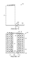
- FIG. 1 is a partial sectional view of an assembly having two coil assemblies, according to embodiments of the present invention
- FIG. 2A is a perspective view of a coil assembly with the insulation layers removed, according to embodiments of the present invention.
- FIG. 2B is a perspective view of a coil assembly, according to embodiments of the present invention.
- FIG. 3A is a perspective view of an outer spring used as part of a coil assembly, according to embodiments of the present invention.
- FIG. 3B is a perspective view of a middle spring used as part of a coil assembly, according to embodiments of the present invention.
- FIG. 3C is a perspective view of an inner spring used as part of a coil assembly, according to embodiments of the present invention.
- FIG. 4A is a top view of a coil assembly, according to embodiments of the present invention.
- FIG. 4B is a sectional view taken along lines A-A of FIG. 4A ;
- FIG. 4C is an enlarged view of the circled portion of FIG. 4B
- FIG. 5 is a side view of a coil assembly, according to embodiments of the present invention.
- FIG. 6 is a bottom view of a sensor board used as part of a coil assembly, according to embodiments of the present invention.
- FIG. 7A is a sectional perspective view of an alternate embodiment of a coil assembly, according to embodiments of the present invention.
- FIG. 7B is a sectional top view of an alternate embodiment of a coil assembly, according to embodiments of the present invention.
- FIG. 7C is a sectional front view of an alternate embodiment of a coil assembly, according to embodiments of the present invention.
- FIG. 7D is a sectional side view of an alternate embodiment of a coil assembly, according to embodiments of the present invention.
- FIG. 1 An assembly having two conductive coil assemblies is shown in FIG. 1 , generally at 10 . Both the first conductive coil assembly, shown generally at 12 , and the second conductive coil assembly, shown generally at 14 , are connected to circuit boards, which in this embodiment is a sensor board 16 and a printed circuit board (PCB) 18 .
- PCB printed circuit board
- the coil assembly 12 includes a first, or inner spring 20 , having a first end 20 A and a second end 20 B.
- the coil assembly 12 also has a middle spring 22 having a first end 22 A and a second end 22 B, and the coil assembly 12 has a third, or outer spring 24 , having a first end 24 A and a second end 24 B.
- the springs 20 , 22 , 24 are concentrically assembled, such that the middle spring 22 is outside of the inner spring 20 , and the outer spring 24 is outside of the middle spring 22 .
- a fourth insulation layer 32 surrounds the outer spring 24 .
- the first end 20 A, 22 A, 24 A of each spring 20 , 22 , 24 is connected to the sensor board 16 and the second end 20 B, 22 B, 24 B of each spring 20 , 22 , 24 is connected to the PCB 18 .
- the inner spring 20 is used for transferring a signal from the sensor board 16 to the PCB 18
- the middle spring 22 is used for supplying power from the PCB 18 to the sensor board 16
- the outer spring 24 is used for providing a ground connection between the sensor board 16 and the PCB 18 .
- Each of the insulation layers 26 , 28 , 30 , 32 electrically isolate the springs 20 , 22 , 24 from one another.
- the insulation layers 26 , 28 , 30 , 32 may be made of a plastic material. However, it is within the scope of the invention that the insulation layers 26 , 28 , 30 , 32 may be made of any suitable material which electrically isolates the springs 20 , 22 , 24 from one another.
- the length 34 of the insulation layers 26 , 28 , 30 , 32 is similar to that of the springs 20 , 22 , 24 , but in alternate embodiments, the length of the insulation layers 26 , 28 , 30 , 32 may be less than that of the springs 20 , 22 , 24 , as long as the insulation layers 26 , 28 , 30 , 32 electrically isolate the springs 20 , 22 , 24 from one another.
- one or more of the insulation layers 26 , 28 , 30 , 32 may be integrally formed with a housing. It is also within the scope of the invention in other alternate embodiments that any other type of separating element made of a suitable material may be used to electrically isolate the springs.
- the sensor board 16 has concentric circular bond pads for connection with the first ends 20 A, 22 A, 24 A of the springs 20 , 22 , 24
- the PCB 18 also has concentric circular bonds pads for connection with the second ends 20 B, 22 B, 24 B of the springs 20 , 22 , 24 .
- FIG. 6 there is a first circular bond pad 36 A, which is in contact with the first end 20 A of the inner spring 20 of the first coil assembly 12 , a second circular bond pad 36 B which is in contact with the first end 22 A of the middle spring 22 of the first coil assembly 12 , and a third circular bond pad 36 C which is in contact with first end 24 A of the outer spring 24 of the first coil assembly 12 .
- the circular bond pads 36 A, 36 B, 36 C are part of the sensor board 16 .
- the PCB 18 also has corresponding concentric circular bonds pads which are in contact with the ends 20 B, 22 B, 24 B of the springs 20 , 22 , 24 for both of the coil assemblies 12 , 14 .
- the circular bonds pads of the PCB 18 are similar to the circular bond pads 36 A, 36 B, 36 C, 38 of the sensor board 16 .
- the coil assembly 12 is rotatable about an axis 40 , such that the first ends 20 A, 22 A, 24 A of the springs 20 , 22 , 24 may be in contact along any area of the corresponding circular bond pads 36 A, 36 B, 36 C of the sensor board 16 , and the second ends 20 B, 22 B, 24 B may be in contact along any area of the corresponding circular bond pads of the PCB 18 .
- the third spring 24 provides a ground connection between the sensor board 16 and the PCB 18 .
- the third spring 24 blocks electromagnetic fields produced by the first spring 20 and the second spring 22 , providing a “Faraday Cage Effect,” reducing electromagnetic inference with other nearby electrical components.
- FIGS. 7A-7D An alternate embodiment of the conductive coil assembly is shown in FIGS. 7A-7D generally at 12 A, with like numbers referring to like elements.
- there is a lower panel 42 and each of the insulating layers 26 , 28 , 30 , 32 are integrally formed with the lower panel 42 , such that the lower panel 42 and the insulating layers 26 , 28 , 30 , 32 are made of the same material.
- the lower panel 42 has a first aperture 44 A, a second aperture 44 B, and a third aperture 44 C. A portion of the inner spring 20 extends into the first aperture 44 A as shown in FIGS.
- a knuckle portion 46 extends through the aperture 44 A, and the second end 20 B is in contact with an inner surface 42 A of the lower panel 42 .
- a knuckle portion of the middle spring 22 extends through the second aperture 44 B, and a knuckle portion of the outer spring 24 extends through the third aperture 44 C.
- the springs 20 , 22 , 24 are positioned between each of the insulating layers 26 , 28 , 30 , 32 as shown in FIGS. 7A-7D .
- a cap portion not shown, having a similar shape to the lower panel 42 , is then attached to the insulating layers 26 , 28 , 30 , 32 .
- the cap portion may be attached using any suitable connection, such as a snap-fit connection, a weld, or the like.
- the cap portion includes corresponding apertures, similar to the apertures 44 A, 44 B, 44 C, and a knuckle formed in proximity to the first end 20 A, 22 A, 24 A of each spring 20 , 22 , 24 extends through each of the corresponding apertures.
- the conductive coil assembly 12 A may be assembled with the sensor board 16 and the PCB 18 such that the knuckle portion 46 near the second end 20 B of the inner spring 20 is in contact with an area of one of the circular bond pads of the PCB 18 , and the knuckle portion (not shown) near the first end 20 A of the inner spring 20 is in contact with the circular bond pad 36 A of the sensor board 16 .
- the knuckle portion near each of the first ends 22 A, 24 A of the springs 22 , 24 are in contact with the corresponding circular bond pads 36 B, 36 C of the sensor board 16
- the knuckle portion near the second ends 22 B, 24 B of the springs 22 , 24 is in contact with the corresponding circular bond pads of the PCB 18 .
- the coil assembly 12 A is rotatable about the axis 40 , such that the knuckle portion located in proximity to the first ends 20 A, 22 A, 24 A of the springs 20 , 22 , 24 may be in contact along any area of the corresponding circular bond pads 36 A, 36 B, 36 C of the sensor board 16 , and the knuckle portion located in proximity to the second ends 20 B, 22 B, 24 B may be in contact along any area of the corresponding circular bond pads of the PCB 18 .
- the coil assembly 12 A therefore provides electrical communication between the sensor board 16 and the PCB 18 , regardless of how the coil assembly 12 A is rotated and positioned about the axis 40 .
- the springs 20 , 22 , 24 of the coil assembly 12 A are not connected to the bond pads 36 A, 36 B, 36 C, 38 of the sensor board 16 or the bond pads of the PCB 18 as described with the previous embodiment.
- the lower panel 42 may be connected to the PCB 18 in any known suitable manner, such as, but not limited to, connectors having a press-fit, interference fit, a latch, or any other suitable connector.
- the cap portion may be connected to the sensor board 16 in a similar manner.
Landscapes
- Engineering & Computer Science (AREA)
- Power Engineering (AREA)
- Microelectronics & Electronic Packaging (AREA)
- Arrangements For Transmission Of Measured Signals (AREA)
- Measuring Instrument Details And Bridges, And Automatic Balancing Devices (AREA)
Priority Applications (2)
| Application Number | Priority Date | Filing Date | Title |
|---|---|---|---|
| US15/846,128 US10270193B1 (en) | 2017-12-18 | 2017-12-18 | Concentric springs for sensor connection |
| PCT/US2018/066081 WO2019126076A1 (fr) | 2017-12-18 | 2018-12-17 | Ressorts concentriques pour connexion de capteur |
Applications Claiming Priority (1)
| Application Number | Priority Date | Filing Date | Title |
|---|---|---|---|
| US15/846,128 US10270193B1 (en) | 2017-12-18 | 2017-12-18 | Concentric springs for sensor connection |
Publications (1)
| Publication Number | Publication Date |
|---|---|
| US10270193B1 true US10270193B1 (en) | 2019-04-23 |
Family
ID=65033649
Family Applications (1)
| Application Number | Title | Priority Date | Filing Date |
|---|---|---|---|
| US15/846,128 Active US10270193B1 (en) | 2017-12-18 | 2017-12-18 | Concentric springs for sensor connection |
Country Status (2)
| Country | Link |
|---|---|
| US (1) | US10270193B1 (fr) |
| WO (1) | WO2019126076A1 (fr) |
Citations (15)
| Publication number | Priority date | Publication date | Assignee | Title |
|---|---|---|---|---|
| US3950846A (en) * | 1974-09-23 | 1976-04-20 | Xerox Corporation | Method of forming a deformed, integral switching device |
| US4961709A (en) * | 1989-02-13 | 1990-10-09 | Burndy Corporation | Vertical action contact spring |
| US6442039B1 (en) * | 1999-12-03 | 2002-08-27 | Delphi Technologies, Inc. | Metallic microstructure springs and method of making same |
| US6517362B2 (en) * | 2000-09-26 | 2003-02-11 | Yukihiro Hirai | Spiral contactor, semiconductor device inspecting apparatus and electronic part using same, and method of manufacturing the same |
| US6821129B2 (en) * | 2003-01-28 | 2004-11-23 | Alps Electric Co., Ltd. | Connection device for stabilizing a contact with external connectors |
| US6843658B2 (en) * | 2002-04-02 | 2005-01-18 | Citizen Electronics Co., Ltd. | Electric connector for connecting electronic instruments |
| US6887085B2 (en) * | 2002-06-10 | 2005-05-03 | Advanced Systems Japan, Inc. | Terminal for spiral contactor and spiral contactor |
| US7080993B2 (en) * | 2004-03-19 | 2006-07-25 | Alps Electric Co., Ltd. | Spiral contactor, contact sheet having spiral contactor, and connecting device having contact sheet |
| US7219426B2 (en) * | 2003-10-27 | 2007-05-22 | Sumitomo Electric Industries, Ltd. | Method of manufacturing protruding-volute contact |
| US7275562B2 (en) * | 2001-10-17 | 2007-10-02 | Agilent Technologies, Inc. | Extensible spiral for flex circuit |
| US7322831B1 (en) * | 2006-07-18 | 2008-01-29 | Cheng Uei Precision Industry Co., Ltd. | Matrix board-to-board connector |
| US7775808B2 (en) * | 2007-03-13 | 2010-08-17 | Alps Electric Co., Ltd. | Contact sheet with spiral contactors serving as elastic contactors and connecting device including the same |
| US7790987B2 (en) * | 2005-04-27 | 2010-09-07 | Sony Computer Entertainment Inc. | Methods and apparatus for interconnecting a ball grid array to a printed circuit board |
| US7931475B2 (en) * | 2008-03-07 | 2011-04-26 | Joinset Co., Ltd. | Solderable elastic electric contact terminal |
| US9040841B2 (en) * | 2009-11-06 | 2015-05-26 | International Business Machines Corporation | Axiocentric scrubbing land grid array contacts and methods for fabrication |
Family Cites Families (4)
| Publication number | Priority date | Publication date | Assignee | Title |
|---|---|---|---|---|
| JP4990463B2 (ja) * | 2000-05-11 | 2012-08-01 | コンティネンタル・テーベス・アクチエンゲゼルシヤフト・ウント・コンパニー・オッフェネ・ハンデルスゲゼルシヤフト | 圧力センサモジュールを一体化したブレーキ装置 |
| DE102006058694B4 (de) * | 2006-12-13 | 2011-06-16 | Semikron Elektronik Gmbh & Co. Kg | Leistungshalbleitermodul mit Kontaktfedern |
| DE102010014940B4 (de) * | 2010-04-14 | 2013-12-19 | Semikron Elektronik Gmbh & Co. Kg | Leistungshalbleitermodul mit Anschlusselementen |
| JP6384197B2 (ja) * | 2014-08-21 | 2018-09-05 | カシオ計算機株式会社 | 電子機器 |
-
2017
- 2017-12-18 US US15/846,128 patent/US10270193B1/en active Active
-
2018
- 2018-12-17 WO PCT/US2018/066081 patent/WO2019126076A1/fr not_active Ceased
Patent Citations (15)
| Publication number | Priority date | Publication date | Assignee | Title |
|---|---|---|---|---|
| US3950846A (en) * | 1974-09-23 | 1976-04-20 | Xerox Corporation | Method of forming a deformed, integral switching device |
| US4961709A (en) * | 1989-02-13 | 1990-10-09 | Burndy Corporation | Vertical action contact spring |
| US6442039B1 (en) * | 1999-12-03 | 2002-08-27 | Delphi Technologies, Inc. | Metallic microstructure springs and method of making same |
| US6517362B2 (en) * | 2000-09-26 | 2003-02-11 | Yukihiro Hirai | Spiral contactor, semiconductor device inspecting apparatus and electronic part using same, and method of manufacturing the same |
| US7275562B2 (en) * | 2001-10-17 | 2007-10-02 | Agilent Technologies, Inc. | Extensible spiral for flex circuit |
| US6843658B2 (en) * | 2002-04-02 | 2005-01-18 | Citizen Electronics Co., Ltd. | Electric connector for connecting electronic instruments |
| US6887085B2 (en) * | 2002-06-10 | 2005-05-03 | Advanced Systems Japan, Inc. | Terminal for spiral contactor and spiral contactor |
| US6821129B2 (en) * | 2003-01-28 | 2004-11-23 | Alps Electric Co., Ltd. | Connection device for stabilizing a contact with external connectors |
| US7219426B2 (en) * | 2003-10-27 | 2007-05-22 | Sumitomo Electric Industries, Ltd. | Method of manufacturing protruding-volute contact |
| US7080993B2 (en) * | 2004-03-19 | 2006-07-25 | Alps Electric Co., Ltd. | Spiral contactor, contact sheet having spiral contactor, and connecting device having contact sheet |
| US7790987B2 (en) * | 2005-04-27 | 2010-09-07 | Sony Computer Entertainment Inc. | Methods and apparatus for interconnecting a ball grid array to a printed circuit board |
| US7322831B1 (en) * | 2006-07-18 | 2008-01-29 | Cheng Uei Precision Industry Co., Ltd. | Matrix board-to-board connector |
| US7775808B2 (en) * | 2007-03-13 | 2010-08-17 | Alps Electric Co., Ltd. | Contact sheet with spiral contactors serving as elastic contactors and connecting device including the same |
| US7931475B2 (en) * | 2008-03-07 | 2011-04-26 | Joinset Co., Ltd. | Solderable elastic electric contact terminal |
| US9040841B2 (en) * | 2009-11-06 | 2015-05-26 | International Business Machines Corporation | Axiocentric scrubbing land grid array contacts and methods for fabrication |
Also Published As
| Publication number | Publication date |
|---|---|
| WO2019126076A1 (fr) | 2019-06-27 |
Similar Documents
| Publication | Publication Date | Title |
|---|---|---|
| CN103378495B (zh) | 电路板和电线组件 | |
| US10312612B2 (en) | High-current connector and high-current connection device | |
| US9774111B2 (en) | Cable connector assembly with multi-layered circuit board | |
| KR101465921B1 (ko) | 차동 데이터 전송용 플러그 커넥터 | |
| US10923855B2 (en) | Connector to prevent misconnection of contacts without the use of a projection and a groove | |
| CN105375167B (zh) | 同轴连接器 | |
| CN107210564A (zh) | 连接端子以及端子连接结构 | |
| EP3881397A1 (fr) | Connecteur de carte de circuit imprimé | |
| CN112913090A (zh) | 同轴连接器装置 | |
| JP6537621B2 (ja) | プリント回路基板アセンブリ | |
| WO2018229152A1 (fr) | Ensemble connecteur | |
| US12456830B2 (en) | Connector | |
| JP4971857B2 (ja) | コネクタ装置 | |
| US9949368B2 (en) | Resin substrate and electronic device | |
| US7445459B2 (en) | Electrical connector with movable contact | |
| JP2014053223A (ja) | 同軸コネクタ | |
| US10270193B1 (en) | Concentric springs for sensor connection | |
| US8951049B2 (en) | Electrical connector assembly with an adaptor for electrical connecting the electrical connector and the PCB | |
| KR20060046535A (ko) | 커넥터용 기판 | |
| US10483703B2 (en) | Connector | |
| US9515398B2 (en) | Mechanical spacer with non-spring electrical connections for a multiple printed circuit board assembly | |
| CN112204678A (zh) | 分流电阻器以及分流电阻器安装结构 | |
| US11018458B2 (en) | Electrical connector with an electromagnetic shielding mechanism | |
| TWI606644B (zh) | 連接器裝置 | |
| CN102655307A (zh) | 用于电子模块的电连接器 |
Legal Events
| Date | Code | Title | Description |
|---|---|---|---|
| FEPP | Fee payment procedure |
Free format text: ENTITY STATUS SET TO UNDISCOUNTED (ORIGINAL EVENT CODE: BIG.); ENTITY STATUS OF PATENT OWNER: LARGE ENTITY |
|
| STCF | Information on status: patent grant |
Free format text: PATENTED CASE |
|
| MAFP | Maintenance fee payment |
Free format text: PAYMENT OF MAINTENANCE FEE, 4TH YEAR, LARGE ENTITY (ORIGINAL EVENT CODE: M1551); ENTITY STATUS OF PATENT OWNER: LARGE ENTITY Year of fee payment: 4 |