US10276112B2 - Mura phenomenon compensation method of display panel and display panel - Google Patents
Mura phenomenon compensation method of display panel and display panel Download PDFInfo
- Publication number
- US10276112B2 US10276112B2 US15/552,273 US201715552273A US10276112B2 US 10276112 B2 US10276112 B2 US 10276112B2 US 201715552273 A US201715552273 A US 201715552273A US 10276112 B2 US10276112 B2 US 10276112B2
- Authority
- US
- United States
- Prior art keywords
- pixels
- region
- mura compensation
- display panel
- mura
- Prior art date
- Legal status (The legal status is an assumption and is not a legal conclusion. Google has not performed a legal analysis and makes no representation as to the accuracy of the status listed.)
- Active
Links
- 238000000034 method Methods 0.000 title claims abstract description 29
- 230000006835 compression Effects 0.000 claims abstract description 11
- 238000007906 compression Methods 0.000 claims abstract description 11
- 102000002067 Protein Subunits Human genes 0.000 claims description 2
- 108010001267 Protein Subunits Proteins 0.000 claims description 2
- 238000004364 calculation method Methods 0.000 description 5
- 238000010586 diagram Methods 0.000 description 4
- 239000004973 liquid crystal related substance Substances 0.000 description 4
- 230000000694 effects Effects 0.000 description 2
- 241001270131 Agaricus moelleri Species 0.000 description 1
- 238000013500 data storage Methods 0.000 description 1
- 230000007547 defect Effects 0.000 description 1
- 230000000750 progressive effect Effects 0.000 description 1
- 230000001737 promoting effect Effects 0.000 description 1
Images



Classifications
-
- G—PHYSICS
- G09—EDUCATION; CRYPTOGRAPHY; DISPLAY; ADVERTISING; SEALS
- G09G—ARRANGEMENTS OR CIRCUITS FOR CONTROL OF INDICATING DEVICES USING STATIC MEANS TO PRESENT VARIABLE INFORMATION
- G09G3/00—Control arrangements or circuits, of interest only in connection with visual indicators other than cathode-ray tubes
- G09G3/20—Control arrangements or circuits, of interest only in connection with visual indicators other than cathode-ray tubes for presentation of an assembly of a number of characters, e.g. a page, by composing the assembly by combination of individual elements arranged in a matrix no fixed position being assigned to or needed to be assigned to the individual characters or partial characters
- G09G3/34—Control arrangements or circuits, of interest only in connection with visual indicators other than cathode-ray tubes for presentation of an assembly of a number of characters, e.g. a page, by composing the assembly by combination of individual elements arranged in a matrix no fixed position being assigned to or needed to be assigned to the individual characters or partial characters by control of light from an independent source
- G09G3/36—Control arrangements or circuits, of interest only in connection with visual indicators other than cathode-ray tubes for presentation of an assembly of a number of characters, e.g. a page, by composing the assembly by combination of individual elements arranged in a matrix no fixed position being assigned to or needed to be assigned to the individual characters or partial characters by control of light from an independent source using liquid crystals
- G09G3/3611—Control of matrices with row and column drivers
-
- G—PHYSICS
- G09—EDUCATION; CRYPTOGRAPHY; DISPLAY; ADVERTISING; SEALS
- G09G—ARRANGEMENTS OR CIRCUITS FOR CONTROL OF INDICATING DEVICES USING STATIC MEANS TO PRESENT VARIABLE INFORMATION
- G09G3/00—Control arrangements or circuits, of interest only in connection with visual indicators other than cathode-ray tubes
- G09G3/006—Electronic inspection or testing of displays and display drivers, e.g. of LED or LCD displays
-
- G—PHYSICS
- G09—EDUCATION; CRYPTOGRAPHY; DISPLAY; ADVERTISING; SEALS
- G09G—ARRANGEMENTS OR CIRCUITS FOR CONTROL OF INDICATING DEVICES USING STATIC MEANS TO PRESENT VARIABLE INFORMATION
- G09G3/00—Control arrangements or circuits, of interest only in connection with visual indicators other than cathode-ray tubes
- G09G3/20—Control arrangements or circuits, of interest only in connection with visual indicators other than cathode-ray tubes for presentation of an assembly of a number of characters, e.g. a page, by composing the assembly by combination of individual elements arranged in a matrix no fixed position being assigned to or needed to be assigned to the individual characters or partial characters
- G09G3/22—Control arrangements or circuits, of interest only in connection with visual indicators other than cathode-ray tubes for presentation of an assembly of a number of characters, e.g. a page, by composing the assembly by combination of individual elements arranged in a matrix no fixed position being assigned to or needed to be assigned to the individual characters or partial characters using controlled light sources
-
- G—PHYSICS
- G09—EDUCATION; CRYPTOGRAPHY; DISPLAY; ADVERTISING; SEALS
- G09G—ARRANGEMENTS OR CIRCUITS FOR CONTROL OF INDICATING DEVICES USING STATIC MEANS TO PRESENT VARIABLE INFORMATION
- G09G2320/00—Control of display operating conditions
- G09G2320/02—Improving the quality of display appearance
- G09G2320/0233—Improving the luminance or brightness uniformity across the screen
-
- G—PHYSICS
- G09—EDUCATION; CRYPTOGRAPHY; DISPLAY; ADVERTISING; SEALS
- G09G—ARRANGEMENTS OR CIRCUITS FOR CONTROL OF INDICATING DEVICES USING STATIC MEANS TO PRESENT VARIABLE INFORMATION
- G09G2320/00—Control of display operating conditions
- G09G2320/02—Improving the quality of display appearance
- G09G2320/0285—Improving the quality of display appearance using tables for spatial correction of display data
-
- G—PHYSICS
- G09—EDUCATION; CRYPTOGRAPHY; DISPLAY; ADVERTISING; SEALS
- G09G—ARRANGEMENTS OR CIRCUITS FOR CONTROL OF INDICATING DEVICES USING STATIC MEANS TO PRESENT VARIABLE INFORMATION
- G09G2360/00—Aspects of the architecture of display systems
- G09G2360/16—Calculation or use of calculated indices related to luminance levels in display data
Definitions
- the present invention relates to a display technology field, and more particularly to a mura phenomenon compensation method of a display panel and the display panel.
- the general reverse compensation data is stored in the data memory (flash). Meanwhile, in order to reduce the design cost, the data memory does not store the gray-level compensation data for each pixel.
- the general practice is to implement compression for regions of n*n pixels (such as 8*8 pixels).
- the gray scale compensation data for one pixel is stored in the data memory for each region.
- the gray scale compensation data of other pixels in the region is calculated by linear interpolation.
- the display panel (3840*2160 pixels UHD, representing regions of 3840 pixels and 2160 pixels) of (Ultra High Definition) resolution is described as an example. Please refer to FIG. 1 .
- the compression is implemented for 8*8 pixels to form 480*270 regions (the square dotted line in figure forms one region).
- the data memory stores the mura compensation data corresponding to the pixels (marked with circles) at the intersection positions of the 1st row of pixels, the 9th row of pixels, the 17th row of pixels, . . . , the 2145th row of pixels, and the 2153th row of pixels with the 1st column of pixels, the 9th column of pixels, the 17th column of pixels, . . .
- the 3825th column of pixels, and the 3833th column of pixels which includes 480*270 mura compensation data.
- the mura compensation data corresponding to the 3841th column of the pixel is calculated and obtained with the stored mura compensation data corresponding to the 3825th column of pixels and the stored mura compensation data corresponding to the 3833th column of pixels to have 270 mura compensation data.
- the mura compensation data corresponding to the 2161th row of the pixel (the virtual pixels marked in the circles) is calculated and obtained with the stored mura compensation data corresponding to the 2145th row of pixels and the stored mura compensation data corresponding to the 2153th row of pixels to have 480 mura compensation data. Accordingly, the data memory needs to store a total of 481*271 mura compensation data.
- the mura compensation data of the other pixels is calculated and obtained by the linear interpolation of the sequence controller (Tcon IC) according to the present 481*271 mura compensation data.
- the mura compensation value corresponding to the pixel at the intersection of the 1st column of pixels and the 1st row of pixels is A′
- the mura compensation value corresponding to the pixel at the intersection of the 9st column of pixels and the 1st row of pixels is B′
- the mura compensation value corresponding to the pixel at the intersection of the 1st column of pixels and the 9st row of pixels is C′
- the mura compensation value corresponding to the pixel at the intersection of the 9st column of pixels and the 9st row of pixels is D′
- the mura compensation value corresponding to the pixel e′ is E′
- the mura compensation value corresponding to the pixel f′ is F′
- the mura compensation value corresponding to the pixel g′ is G′
- X′ and Y′ are the row number and the column number of the corresponding pixel relative to the pixel at the crossing position of the first column and the first row.
- the mura compensation data calculation of the 3834th column to the 3840th column of pixels and the 2154th row to the 2160th row of pixels requires the mura compensation data corresponding to the 3841th column of pixels and the 2161th row of pixels. Therefore, 481*271 mura compensation data need to be stored. Because the data memory needs storing 481*271 mura compensation data, the amount of data stored is larger, resulting in that the data storage space of the data memory needs to be larger, thus increasing the cost.
- the technical issue that the embodiment of the present invention solves is to provide a mura phenomenon compensation method of a display panel and the display panel.
- the present application can reduce the display panel storage space.
- the present invention first provides a mura phenomenon compensation method of a display panel, comprising:
- n*m pixels implementing compression for a region of n*m pixels to store a mura compensation value corresponding to a center pixel of each region, wherein the mura compensation value of the center pixel of at least one region is an average mura compensation value of a corresponding region, and n and m are integers larger than or equal to 2;
- the mura compensation value corresponding to the center pixel of each region is the average mura compensation value of the corresponding region.
- the step of obtaining mura compensation values corresponding to the other pixels except the center pixel according to the stored mura compensation value comprises:
- the method further comprises steps of:
- obtaining the mura compensation values corresponding to the other pixels by linearly interpolating the mura compensation value corresponding to the center pixel of the region, where the other pixels are located and a mura compensation value corresponding to a center pixel of an adjacent region.
- the display panel comprises a plurality of special regions at edges, and the special regions comprises pixels of n*a or b*m, wherein a is less than m and a is a positive integer, and b is less than n and b is a positive integer, and the method further comprises steps of:
- the present invention provides a display panel, comprising:
- a storage unit implementing compression for a region of n*m pixels to store a mura compensation value corresponding to a center pixel of each region, wherein the mura compensation value of the center pixel of at least one region is an average mura compensation value of a corresponding region, and n and m are integers larger than or equal to 2;
- a processing unit obtaining mura compensation values corresponding to other pixels except the center pixel according to the stored mura compensation value.
- the mura compensation value corresponding to the center pixel of each region is the average mura compensation value of the corresponding region.
- processing unit comprises:
- a determining unit determining whether the other pixels are located outside a row or a column, where an outermost center pixel of the display panel is located;
- a processing sub unit if a determination of the determining unit is yes, taking the mura compensation value corresponding to the center pixel of the region, where the other pixels are located as the mura compensation values corresponding to the other pixels; if the determination of the determining unit is no, obtaining the mura compensation values corresponding to the other pixels by linearly interpolating the mura compensation value corresponding to the center pixel of the region, where the other pixels are located and a mura compensation value corresponding to a center pixel of an adjacent region.
- the benefits are: since the mura compensation values stored in the display panel are reduced relative to the prior art, the display panel storage space can be reduced, so that the cost can be reduced.
- FIG. 1 is an arrangement diagram of pixels of a display panel according to prior art (the display panel stores the mura compensation values of the pixels in the circles);
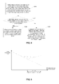
- FIG. 2 is a flowchart of a mura phenomenon compensation method of a display panel according to one embodiment of the present invention
- FIG. 3 is an arrangement diagram of pixels of a display panel according to one embodiment of the present invention (the display panel stores the mura compensation values of the pixels in the circles);
- FIG. 4 is a flowchart of a mura phenomenon compensation method of a display panel according to another embodiment of the present invention.
- FIG. 5 is a comparison diagram of a mura compensation line (solid line) for one row/column of pixels according to the another embodiment of the present invention, a mura compensation line (dot dash line) for one row/column of pixels according to prior art and a mura compensation line (dotted line) actually required for one row/column of pixels;
- FIG. 6 is a flowchart of a mura phenomenon compensation method of a display panel according to one another embodiment of the present invention.
- FIG. 7 is a composition diagram of a display panel according to one embodiment of the present invention.
- the terms “including” and “having” and their any deformations are intended to cover non-exclusive inclusion.
- a process, a method, a system, a product or a device comprising a series of steps or units which is not limited to the steps or units already listed, but optionally further comprises steps or units which are not listed, or optionally further comprises other steps or units which are inherent in these the process, the method, the product or the device.
- the terminologies “first”, “second” and “third” are used for distinguishing different objects but not for describing the specific sequence.
- the embodiment of the present invention provides a mura phenomenon compensation method of a display panel.
- the display panel may be a liquid crystal display panel or other display panel.
- the display panel is described as an example of a UHD (Ultra High Definition) display panel. Namely, the resolution of the display panel reaches up to 3840*2160 (the resolution 3840*2160 is illustrated for the following description).
- the resolution of the display panel is not limited to the aforesaid resolution but may also be 1920*1080 resolution or other resolutions. Please refer to FIG. 2 and FIG. 3 .
- the method comprises steps of:
- n m
- n and m are both 8.
- n and m may not be equal, and the n and m may also be other integers larger than or equal to 2.
- FIG. 3 one dashed box is one region.
- the display panel stores a mura compensation value corresponding to a center pixel (the center pixels in FIG. 3 are marked in circles) of each region. Because there are only 480*270 regions, the display panel only needs to store 480*270 mura compensation values.
- FIG. 3 the region at the top left corner of the display panel is illustrated for explanation. The region is arranged with the first column of pixels C 1 to the eighth column of pixels C 8 and the first row of pixels R 1 to the eighth row of pixels R 8 .
- the center pixel of the region can be the pixel at the intersection of the fourth row of pixels R 4 and the fourth column of pixels C 4 , or can be the pixel at the intersection of the fourth row of pixels R 4 and the fifth column of pixels C 5 , or can be the pixel at the intersection of the fifth row of pixels R 5 and the fourth column of pixels C 4 , or can be the pixel at the intersection of the fifth row of pixels R 5 and the fifth column of pixels C 5 .
- the pixel at the intersection of the fourth row of pixels R 4 and the fourth column of pixels C 4 is the center pixel (marked in circle in FIG. 3 ).
- the settings of the center pixels in other regions of the display panel also refer to the center pixel position of this region. Certainly, in other embodiments of the present invention, when a center pixel is present in the region, the center pixel is the most central pixel.
- the mura compensation value of the center pixel of at least one region is an average mura compensation value of a corresponding region.
- the mura compensation value of the center pixel is a sum of the mura compensation values for all the pixels of the region divided by 64.
- the mura compensation value corresponding to the center pixel of each region is the average mura compensation value of the corresponding region.
- the average mura compensation value is obtained by an external mura repair system and then correspondingly stored in the display panel.
- the mura compensation value of the center pixel may also be the actual mura compensation value of the pixel, rather than the average mura compensation value of the corresponding region.
- the pixels in the same region that the display panel is implemented with compression comprise a center pixel and other pixels.
- the mura compensation values corresponding to the other pixels can be obtained according to the stored 480*270 mura compensation values.
- the mura compensation values corresponding to the other pixels can be obtained by linear interpolation, or the mura compensation values corresponding to the other pixels of some special positions are directly given with the mura compensation value of the center pixel of the region. Then, the mura compensation value of the center pixel of the region is the average mura compensation value of the corresponding region.
- the mura compensation values stored in the display panel are reduced relative to the prior art. Specifically, there are 480*270 mura compensation values stored in this embodiment. There are 481*271 values need to be stored in prior art. Thus, the storage space of the display panel can be reduced to decrease the cost.
- step S 120 of obtaining mura compensation values corresponding to the other pixels except the center pixel according to the stored mura compensation value specifically comprises:
- step S 121 determining whether the other pixels are located outside a row or a column, where an outermost center pixel of the display panel is located, and if yes, step S 122 is executed, and if not, step S 123 is executed.
- the display panel is square.
- the outermost sides of the display panel comprise a left side, a right side, an upper side and a lower side.
- the row or column, where the center pixel at the outermost side of the display panel is located is column 4 in the left side, and is column 3836 in the right side, and is row 4 in upper side, and is row 2156 in the lower side. determining whether the other pixels are located in regions outside a row or a column, where an outermost center pixel of the display panel is located is to determine whether the other pixels are located in positions outside the region surrounded by the 4th column of pixels, the 3836th column of pixels, the 4th row of pixels, and the 2156th row of pixels.
- the other pixels are located in the 1st column to the 3rd column of pixels, in the 3837th column to the 3840th column of pixels, in the 1st row to the 3rd row of pixels and in the 2157th row to the 2160th row of pixels of the display panel, such as the coordinates of the other pixels are (1,1) (representing the pixels at the intersection of the first column of pixels and the first row of pixels, that is, the pixel at the top left), (1,2160) (representing the column coordinate and the row coordinate), (3840,1), (3840,2160), (3,4) and (4,3).
- the mura compensation value corresponding to the center pixel of the region, where the other pixels are located are taken as the mura compensation values corresponding to the other pixels.
- the mura compensation value corresponding to the center pixel of the region at the top left is given as the mura compensation value corresponding to the pixel with the coordinate (1,1).
- the mura compensation value corresponding to the center pixel with the coordinate (4,4) is given as the mura compensation value corresponding to the pixel with the coordinate (1,1).
- the mura compensation value corresponding to the center pixel is the average mura compensation value of the corresponding region, thus taking the mura compensation value as the mura compensation values corresponding to the other pixels will not cause the uneven brightness.
- obtaining the mura compensation data of the 3834th column to the 3840th column of pixels and the 2154th row to the 2160th row of pixels needs the mura compensation data corresponding to the 3841th of pixels and the 2161th row of pixels (the pixels marked in circles).
- the mura compensation data of the 3841th of pixels and the 2161th row of pixels themselves are not accurate (these pixels are virtual pixels, which are obtained by calculation)
- the calculated mura compensation data for the other pixels at the 3834th column to the 3840th column of pixels and the 2154th row to the 2160th row of pixels are more inaccurate to result in the uneven brightness issue.
- the mura compensation result of this embodiment is better and is more close to the mura compensation value which is actually required to promote the screen effect of the display panel.
- the display panel does not have to store some of the compensation data as much as in the prior art.
- the display panel may also be subjected to other processes, and it is also possible not to store some of the compensation data as much as in the prior art.
- the other pixels can be covered by a side frame.
- the four edges may easily have light leakage after the module is assembled in prior art, which will also influence the calculation accuracy of the mura compensation data of pixels of the first row and the first column.
- the compensation values of the pixels at the edges of the display panel are directly given with the average mura compensation values of the corresponding regions, so the brightness at the edges is more even.
- the mura compensation values corresponding to the other pixels are obtained by linearly interpolating the mura compensation value corresponding to the center pixel of the region, where the other pixels are located and a mura compensation value corresponding to a center pixel of an adjacent region.
- E [(8 ⁇ Y )* A+Y*C ]/8
- F [(8 ⁇ Y )* B+Y*D ]/8
- G [(8 ⁇ X )* E+X*F ]/8.
- X and Y are the row number and the column number of the corresponding pixel relative to the center pixel (4, 4), respectively.
- the mura compensation values corresponding to the other pixels which are not located in the 1st column to the 3rd column of pixels, in the 3837th column to the 3840th column of pixels, in the 1st row to the 3rd row of pixels and in the 2157th row to the 2160th row of pixels of the display panel can be obtained by linear interpolation, thus the mura compensation values corresponding to the pixels in the entire display panel can be obtained.
- the display panel comprises a plurality of special regions at edges, and the special regions comprises pixels of n*a or b*m, wherein a is less than m and a is a positive integer, and b is less than n and b is a positive integer.
- the mura phenomenon compensation method of the display panel further comprises except step 110 , and step S 120 :
- the coordinate of the center pixel can be (4,3) or (5,3), i.e the pixel at the intersect of the 4th column of pixels and the 3rd row of pixels or the pixel at the intersect of the 5th column of pixels and the 3rd row of pixels
- the average mura compensation value is a sum of the mura compensation values corresponding to all the pixels in the corresponding special region divided by 40.
- the mura compensation values corresponding to the other pixels in the special regions can be processed with reference to S 122 and S 123 , and are not described here.
- the embodiment of the present invention further provides a display panel. Please refer to FIG. 7 .
- the display panel comprises:
- a storage unit 110 implementing compression for a region of n*m pixels to store a mura compensation value corresponding to a center pixel of each region, wherein the mura compensation value of the center pixel of at least one region is an average mura compensation value of a corresponding region, and n and m are integers larger than or equal to 2;
- the storage unit 110 is a data memory (flash) but the present invention is not limited thereto. In other embodiments of the present invention, the storage unit may also be a sequence controller (Tcon IC). In this embodiment, the mura compensation value corresponding to the center pixel of each region is the average mura compensation value of the corresponding region.
- a processing unit 120 obtaining mura compensation values corresponding to other pixels except the center pixel according to the stored mura compensation value.
- the processing unit 120 is a sequence controller (Tcon IC).
- the processing unit specifically comprises:
- a determining unit 121 determining whether the other pixels are located outside a row or a column, where an outermost center pixel of the display panel is located;
- a processing sub unit 122 if a determination of the determining unit 121 is yes, taking the mura compensation value corresponding to the center pixel of the region, where the other pixels are located as the mura compensation values corresponding to the other pixels, and if the determination of the determining unit 121 is no, obtaining the mura compensation values corresponding to the other pixels by linearly interpolating the mura compensation value corresponding to the center pixel of the region, where the other pixels are located and a mura compensation value corresponding to a center pixel of an adjacent region.
- each of the embodiments in the specification is described in a progressive manner, and each embodiment focuses on the differences from other embodiments, and the same or similar parts among the various embodiments can be referred to one another.
- the embodiment of the device it is basically similar with the embodiment of method, so the description is simpler, and the related parts can be referred to the description of the embodiment of method.
- the display panel storage space can be reduced, so that the cost can be reduced.
Landscapes
- Engineering & Computer Science (AREA)
- Physics & Mathematics (AREA)
- Computer Hardware Design (AREA)
- General Physics & Mathematics (AREA)
- Theoretical Computer Science (AREA)
- Chemical & Material Sciences (AREA)
- Crystallography & Structural Chemistry (AREA)
- Control Of Indicators Other Than Cathode Ray Tubes (AREA)
- Liquid Crystal Display Device Control (AREA)
Applications Claiming Priority (3)
| Application Number | Priority Date | Filing Date | Title |
|---|---|---|---|
| CN201710305591.7A CN106952627B (zh) | 2017-05-03 | 2017-05-03 | 一种显示面板的mura现象补偿方法及显示面板 |
| CN201710305591.7 | 2017-05-03 | ||
| PCT/CN2017/083823 WO2018201512A1 (fr) | 2017-05-03 | 2017-05-10 | Procédé de compensation de défaut mura d'un panneau d'affichage, et panneau d'affichage |
Publications (2)
| Publication Number | Publication Date |
|---|---|
| US20180330682A1 US20180330682A1 (en) | 2018-11-15 |
| US10276112B2 true US10276112B2 (en) | 2019-04-30 |
Family
ID=59477943
Family Applications (1)
| Application Number | Title | Priority Date | Filing Date |
|---|---|---|---|
| US15/552,273 Active US10276112B2 (en) | 2017-05-03 | 2017-05-10 | Mura phenomenon compensation method of display panel and display panel |
Country Status (6)
| Country | Link |
|---|---|
| US (1) | US10276112B2 (fr) |
| EP (1) | EP3640930B1 (fr) |
| JP (1) | JP2020522726A (fr) |
| KR (1) | KR102257160B1 (fr) |
| CN (1) | CN106952627B (fr) |
| WO (1) | WO2018201512A1 (fr) |
Cited By (2)
| Publication number | Priority date | Publication date | Assignee | Title |
|---|---|---|---|---|
| US11335253B2 (en) | 2018-02-27 | 2022-05-17 | Chengdu Boe Optoelectronics Technology Co., Ltd. | Optical compensation method for display panel and optical compensation device |
| US12217721B2 (en) | 2021-11-11 | 2025-02-04 | Samsung Electronics Co., Ltd. | Mura inspection device for compressing mura data through dimensionality reduction, operating method, and display system including the same |
Families Citing this family (29)
| Publication number | Priority date | Publication date | Assignee | Title |
|---|---|---|---|---|
| CN107240384B (zh) * | 2017-08-11 | 2019-04-05 | 芯颖科技有限公司 | 显示器亮度补偿方法及装置 |
| CN107731194A (zh) * | 2017-11-21 | 2018-02-23 | 深圳市华星光电半导体显示技术有限公司 | 一种mura补偿方法及装置 |
| KR102441479B1 (ko) * | 2017-12-27 | 2022-09-13 | 삼성디스플레이 주식회사 | 표시 장치 및 표시 장치의 구동 방법 |
| CN109119035A (zh) | 2018-07-24 | 2019-01-01 | 深圳市华星光电半导体显示技术有限公司 | mura补偿方法及mura补偿系统 |
| CN108877631B (zh) * | 2018-07-25 | 2021-09-10 | 昆山国显光电有限公司 | 显示屏的Mura补偿方法、装置、计算机设备及存储介质 |
| CN110176210B (zh) | 2018-07-27 | 2021-04-27 | 京东方科技集团股份有限公司 | 显示驱动、压缩解压缩方法及装置、显示装置、存储介质 |
| CN111341271B (zh) * | 2018-12-19 | 2021-07-16 | 咸阳彩虹光电科技有限公司 | 一种显示装置的灰阶补偿方法和装置 |
| CN112017590A (zh) * | 2019-05-28 | 2020-12-01 | 陕西坤同半导体科技有限公司 | 显示面板的Mura补偿方法、装置、介质及电子设备 |
| CN112216236A (zh) * | 2019-07-09 | 2021-01-12 | 陕西坤同半导体科技有限公司 | 一种显示面板补偿方法、装置及系统 |
| CN110634435A (zh) * | 2019-09-24 | 2019-12-31 | 武汉天马微电子有限公司 | 显示面板的补偿处理方法及补偿处理装置 |
| CN110689846B (zh) * | 2019-11-06 | 2021-03-30 | 昆山国显光电有限公司 | 一种像素灰阶补偿参数压缩存储方法、装置和存储介质 |
| KR102692179B1 (ko) * | 2019-12-26 | 2024-08-06 | 주식회사 엘엑스세미콘 | 무라 보상 회로 및 그를 채용한 디스플레이를 위한 구동 장치 |
| CN111276083B (zh) * | 2020-01-16 | 2021-08-31 | 深圳市爱协生科技有限公司 | Demura Table数据压缩方法和解压缩方法 |
| CN111968563B (zh) * | 2020-09-08 | 2024-04-05 | 京东方科技集团股份有限公司 | 显示面板的亮度补偿方法、装置、系统、显示面板及介质 |
| KR102826935B1 (ko) * | 2020-11-13 | 2025-07-01 | 삼성디스플레이 주식회사 | 표시장치 |
| KR102895209B1 (ko) | 2020-12-02 | 2025-12-05 | 주식회사 엘엑스세미콘 | 무라 보상을 위한 무라 보상장치 및 데이터처리회로 |
| CN112770096B (zh) * | 2020-12-31 | 2024-02-09 | 深圳Tcl数字技术有限公司 | 图像处理方法、装置、终端设备以及计算机可读存储介质 |
| CN112967675B (zh) * | 2021-02-24 | 2022-04-01 | Tcl华星光电技术有限公司 | 一种显示面板驱动方法、显示装置及驱动装置 |
| CN113327551A (zh) * | 2021-06-16 | 2021-08-31 | 云谷(固安)科技有限公司 | 显示面板的补偿方法、补偿装置及显示装置 |
| CN113593494B (zh) * | 2021-07-19 | 2022-07-12 | Tcl华星光电技术有限公司 | 显示补偿方法及装置、显示面板 |
| CN113658536B (zh) * | 2021-08-17 | 2024-04-26 | 苏州华兴源创科技股份有限公司 | 像素点补偿数据的存储方法和像素点补偿方法 |
| CN113674719A (zh) * | 2021-08-17 | 2021-11-19 | 晟合微电子(肇庆)有限公司 | Mura补偿信息生成方法、装置、设备、介质及Mura补偿方法 |
| KR20230037212A (ko) * | 2021-09-09 | 2023-03-16 | 주식회사 엘엑스세미콘 | 디-무라를 위한 보상 정보 제공 장치 및 방법과 보상 정보를 이용하는 디스플레이 구동 장치 |
| CN114170334B (zh) * | 2021-12-08 | 2025-04-11 | 北京欧铼德微电子技术有限公司 | 补偿数据的压缩方法及装置、电子设备和存储介质 |
| CN114613329B (zh) * | 2022-03-29 | 2024-03-26 | 合肥维信诺科技有限公司 | 数据处理方法和装置、亮度补偿方法和装置 |
| CN115878040A (zh) * | 2022-12-19 | 2023-03-31 | 惠科股份有限公司 | 外部补偿数据存储方法及装置、显示装置 |
| CN116682352B (zh) * | 2023-06-26 | 2026-04-17 | 合肥维信诺科技有限公司 | 显示面板的数据处理方法、装置及计算机可读存储介质 |
| CN117995112B (zh) * | 2024-04-01 | 2024-05-31 | 瑞旦微电子技术(上海)有限公司 | 一种基于自适应矩形分块的Demura数据处理方法及显示装置 |
| CN119626138B (zh) * | 2025-01-23 | 2025-10-28 | 合肥维信诺科技有限公司 | 数据处理方法、装置、设备及介质 |
Citations (11)
| Publication number | Priority date | Publication date | Assignee | Title |
|---|---|---|---|---|
| US20080284794A1 (en) | 2007-05-17 | 2008-11-20 | Top Team Int'l Patent & Trademark Office | Image display system and method for eliminating mura defects |
| US20090135211A1 (en) | 2007-11-26 | 2009-05-28 | Tpo Displays Corp. | Image displaying system and method for eliminating mura defect |
| US20140184671A1 (en) * | 2012-12-28 | 2014-07-03 | Gil-Jae Lee | Display device, and optical compensation system and optical compensation method thereof |
| CN104992657A (zh) | 2015-07-27 | 2015-10-21 | 京东方科技集团股份有限公司 | mura补偿模块和方法、显示装置和方法 |
| CN105206239A (zh) | 2015-10-16 | 2015-12-30 | 深圳市华星光电技术有限公司 | Mura现象补偿方法 |
| CN105590604A (zh) | 2016-03-09 | 2016-05-18 | 深圳市华星光电技术有限公司 | Mura现象补偿方法 |
| CN105632443A (zh) | 2016-03-09 | 2016-06-01 | 深圳市华星光电技术有限公司 | Mura现象补偿方法 |
| CN105895043A (zh) | 2016-06-08 | 2016-08-24 | 深圳市华星光电技术有限公司 | 显示面板的Mura补偿方法及Mura补偿装置 |
| US9576541B2 (en) | 2014-11-21 | 2017-02-21 | Samsung Display Co., Ltd. | Vision inspection apparatus and method of compensating gamma defect and mura defect thereof |
| US20170332090A1 (en) * | 2016-05-13 | 2017-11-16 | Synaptics Japan Gk | Device and method for block compression and block decompression |
| US20180204528A1 (en) * | 2015-07-31 | 2018-07-19 | Sony Corporation | Image signal processing device, image signal processing method, and display apparatus |
Family Cites Families (7)
| Publication number | Priority date | Publication date | Assignee | Title |
|---|---|---|---|---|
| JP2002162930A (ja) * | 2000-11-22 | 2002-06-07 | Sharp Corp | 画像処理装置および画像処理方法 |
| KR100825098B1 (ko) * | 2001-12-17 | 2008-04-25 | 삼성전자주식회사 | 액정 표시 장치의 구동 장치 및 구동 방법 |
| WO2003071794A1 (fr) * | 2002-02-19 | 2003-08-28 | Olympus Corporation | Procede et dispositif de calcul de donnees de correction d'image et systeme de projection |
| KR100590529B1 (ko) * | 2003-11-04 | 2006-06-15 | 삼성전자주식회사 | 영상의 국부적 휘도 향상 방법 및 장치와 컴퓨터프로그램을 저장하는 컴퓨터로 읽을 수 있는 기록 매체 |
| JP2006330312A (ja) * | 2005-05-26 | 2006-12-07 | Hitachi Ltd | 画像表示装置 |
| TWI536341B (zh) * | 2014-03-21 | 2016-06-01 | 緯創資通股份有限公司 | 顯示補償方法與顯示補償系統 |
| CN106339196B (zh) * | 2016-08-31 | 2019-03-15 | 深圳市华星光电技术有限公司 | DeMura表的数据压缩、解压缩方法及Mura补偿方法 |
-
2017
- 2017-05-03 CN CN201710305591.7A patent/CN106952627B/zh active Active
- 2017-05-10 JP JP2019560163A patent/JP2020522726A/ja active Pending
- 2017-05-10 EP EP17908113.8A patent/EP3640930B1/fr active Active
- 2017-05-10 WO PCT/CN2017/083823 patent/WO2018201512A1/fr not_active Ceased
- 2017-05-10 US US15/552,273 patent/US10276112B2/en active Active
- 2017-05-10 KR KR1020197035826A patent/KR102257160B1/ko active Active
Patent Citations (11)
| Publication number | Priority date | Publication date | Assignee | Title |
|---|---|---|---|---|
| US20080284794A1 (en) | 2007-05-17 | 2008-11-20 | Top Team Int'l Patent & Trademark Office | Image display system and method for eliminating mura defects |
| US20090135211A1 (en) | 2007-11-26 | 2009-05-28 | Tpo Displays Corp. | Image displaying system and method for eliminating mura defect |
| US20140184671A1 (en) * | 2012-12-28 | 2014-07-03 | Gil-Jae Lee | Display device, and optical compensation system and optical compensation method thereof |
| US9576541B2 (en) | 2014-11-21 | 2017-02-21 | Samsung Display Co., Ltd. | Vision inspection apparatus and method of compensating gamma defect and mura defect thereof |
| CN104992657A (zh) | 2015-07-27 | 2015-10-21 | 京东方科技集团股份有限公司 | mura补偿模块和方法、显示装置和方法 |
| US20180204528A1 (en) * | 2015-07-31 | 2018-07-19 | Sony Corporation | Image signal processing device, image signal processing method, and display apparatus |
| CN105206239A (zh) | 2015-10-16 | 2015-12-30 | 深圳市华星光电技术有限公司 | Mura现象补偿方法 |
| CN105590604A (zh) | 2016-03-09 | 2016-05-18 | 深圳市华星光电技术有限公司 | Mura现象补偿方法 |
| CN105632443A (zh) | 2016-03-09 | 2016-06-01 | 深圳市华星光电技术有限公司 | Mura现象补偿方法 |
| US20170332090A1 (en) * | 2016-05-13 | 2017-11-16 | Synaptics Japan Gk | Device and method for block compression and block decompression |
| CN105895043A (zh) | 2016-06-08 | 2016-08-24 | 深圳市华星光电技术有限公司 | 显示面板的Mura补偿方法及Mura补偿装置 |
Cited By (2)
| Publication number | Priority date | Publication date | Assignee | Title |
|---|---|---|---|---|
| US11335253B2 (en) | 2018-02-27 | 2022-05-17 | Chengdu Boe Optoelectronics Technology Co., Ltd. | Optical compensation method for display panel and optical compensation device |
| US12217721B2 (en) | 2021-11-11 | 2025-02-04 | Samsung Electronics Co., Ltd. | Mura inspection device for compressing mura data through dimensionality reduction, operating method, and display system including the same |
Also Published As
| Publication number | Publication date |
|---|---|
| KR20190141779A (ko) | 2019-12-24 |
| CN106952627B (zh) | 2019-01-15 |
| EP3640930A1 (fr) | 2020-04-22 |
| US20180330682A1 (en) | 2018-11-15 |
| WO2018201512A1 (fr) | 2018-11-08 |
| EP3640930A4 (fr) | 2020-12-16 |
| EP3640930B1 (fr) | 2025-07-09 |
| KR102257160B1 (ko) | 2021-05-26 |
| CN106952627A (zh) | 2017-07-14 |
| JP2020522726A (ja) | 2020-07-30 |
Similar Documents
| Publication | Publication Date | Title |
|---|---|---|
| US10276112B2 (en) | Mura phenomenon compensation method of display panel and display panel | |
| US10170063B2 (en) | Mura compensation method for display panel and display panel | |
| US10891911B2 (en) | Mura compensation method and mura compensation system for addressing problem of inability to effectively eliminate mura at bright or dark boundary lines after compensation | |
| US11069286B2 (en) | Color compensation method, compensation device, and display device | |
| CN104992657B (zh) | mura补偿模块和方法、显示装置和方法 | |
| JP6625737B2 (ja) | ムラ現象の補償方法 | |
| CN105632443A (zh) | Mura现象补偿方法 | |
| US9972256B2 (en) | LCD panel and driving method thereof | |
| US9390645B2 (en) | Display apparatus and method of driving the same | |
| CN111292701B (zh) | 显示面板补偿方法及装置 | |
| WO2018166266A1 (fr) | Procédé et appareil de réparation de défaut mura sur la base d'une position désignée | |
| US20170140694A1 (en) | Method of Computing Target Values Based On Brightness Switching On A Subpixel Signal | |
| CN115497428B (zh) | 亮度补偿方法、可读存储介质以及显示装置 | |
| US11282478B2 (en) | Image data correcting device, and display device including the same | |
| US11837187B2 (en) | Display panel driving method and driving device, display device, and storage medium | |
| US20170221404A1 (en) | Display apparatus and driving method thereof | |
| JP2017538148A (ja) | 液晶パネル及びその画素単位の設定方法 | |
| CN111276086B (zh) | 显示器及其降低云纹的方法 | |
| US11386822B1 (en) | BD cell display panel, manufacturing method and driving method thereof, and display device | |
| CN118430438A (zh) | 显示面板的补偿方法、装置、设备及介质 | |
| CN112614468B (zh) | 显示面板的亮度补偿方法和系统 | |
| CN110176207B (zh) | 一种图像数据确定方法、装置及电子设备 | |
| US10204538B2 (en) | Image processing circuit and display device including the same | |
| CN117524144A (zh) | 一种显示面板的补偿方法、显示装置和存储介质 | |
| KR20080012030A (ko) | 표시 장치의 구동 장치 및 그 영상 신호 보정 방법 |
Legal Events
| Date | Code | Title | Description |
|---|---|---|---|
| AS | Assignment |
Owner name: SHENZHEN CHINA STAR OPTOELECTRONICS TECHNOLOGY CO. Free format text: ASSIGNMENT OF ASSIGNORS INTEREST;ASSIGNOR:ZHANG, HUA;REEL/FRAME:043608/0015 Effective date: 20170616 |
|
| STPP | Information on status: patent application and granting procedure in general |
Free format text: PUBLICATIONS -- ISSUE FEE PAYMENT VERIFIED |
|
| STCF | Information on status: patent grant |
Free format text: PATENTED CASE |
|
| MAFP | Maintenance fee payment |
Free format text: PAYMENT OF MAINTENANCE FEE, 4TH YEAR, LARGE ENTITY (ORIGINAL EVENT CODE: M1551); ENTITY STATUS OF PATENT OWNER: LARGE ENTITY Year of fee payment: 4 |