US10283597B2 - Scandium-containing III-N etch-stop layers for selective etching of III-nitrides and related materials - Google Patents
Scandium-containing III-N etch-stop layers for selective etching of III-nitrides and related materials Download PDFInfo
- Publication number
- US10283597B2 US10283597B2 US15/807,821 US201715807821A US10283597B2 US 10283597 B2 US10283597 B2 US 10283597B2 US 201715807821 A US201715807821 A US 201715807821A US 10283597 B2 US10283597 B2 US 10283597B2
- Authority
- US
- United States
- Prior art keywords
- etch
- layer
- epitaxial
- stop layer
- iii
- Prior art date
- Legal status (The legal status is an assumption and is not a legal conclusion. Google has not performed a legal analysis and makes no representation as to the accuracy of the status listed.)
- Active
Links
Images


Classifications
-
- H01L29/2003—
-
- H—ELECTRICITY
- H10—SEMICONDUCTOR DEVICES; ELECTRIC SOLID-STATE DEVICES NOT OTHERWISE PROVIDED FOR
- H10D—INORGANIC ELECTRIC SEMICONDUCTOR DEVICES
- H10D62/00—Semiconductor bodies, or regions thereof, of devices having potential barriers
- H10D62/80—Semiconductor bodies, or regions thereof, of devices having potential barriers characterised by the materials
- H10D62/85—Semiconductor bodies, or regions thereof, of devices having potential barriers characterised by the materials being Group III-V materials, e.g. GaAs
- H10D62/8503—Nitride Group III-V materials, e.g. AlN or GaN
-
- H01L21/02378—
-
- H01L21/02439—
-
- H01L21/02458—
-
- H01L21/02502—
-
- H01L21/0254—
-
- H01L21/3065—
-
- H01L21/3081—
-
- H01L29/201—
-
- H—ELECTRICITY
- H10—SEMICONDUCTOR DEVICES; ELECTRIC SOLID-STATE DEVICES NOT OTHERWISE PROVIDED FOR
- H10D—INORGANIC ELECTRIC SEMICONDUCTOR DEVICES
- H10D62/00—Semiconductor bodies, or regions thereof, of devices having potential barriers
- H10D62/80—Semiconductor bodies, or regions thereof, of devices having potential barriers characterised by the materials
- H10D62/85—Semiconductor bodies, or regions thereof, of devices having potential barriers characterised by the materials being Group III-V materials, e.g. GaAs
- H10D62/852—Semiconductor bodies, or regions thereof, of devices having potential barriers characterised by the materials being Group III-V materials, e.g. GaAs being Group III-V materials comprising three or more elements, e.g. AlGaN or InAsSbP
-
- H—ELECTRICITY
- H10—SEMICONDUCTOR DEVICES; ELECTRIC SOLID-STATE DEVICES NOT OTHERWISE PROVIDED FOR
- H10P—GENERIC PROCESSES OR APPARATUS FOR THE MANUFACTURE OR TREATMENT OF DEVICES COVERED BY CLASS H10
- H10P14/00—Formation of materials, e.g. in the shape of layers or pillars
- H10P14/20—Formation of materials, e.g. in the shape of layers or pillars of semiconductor materials
- H10P14/29—Formation of materials, e.g. in the shape of layers or pillars of semiconductor materials characterised by the substrates
- H10P14/2901—Materials
- H10P14/2902—Materials being Group IVA materials
- H10P14/2904—Silicon carbide
-
- H—ELECTRICITY
- H10—SEMICONDUCTOR DEVICES; ELECTRIC SOLID-STATE DEVICES NOT OTHERWISE PROVIDED FOR
- H10P—GENERIC PROCESSES OR APPARATUS FOR THE MANUFACTURE OR TREATMENT OF DEVICES COVERED BY CLASS H10
- H10P14/00—Formation of materials, e.g. in the shape of layers or pillars
- H10P14/20—Formation of materials, e.g. in the shape of layers or pillars of semiconductor materials
- H10P14/32—Formation of materials, e.g. in the shape of layers or pillars of semiconductor materials characterised by intermediate layers between substrates and deposited layers
- H10P14/3202—Materials thereof
- H10P14/3214—Materials thereof being Group IIIA-VA semiconductors
- H10P14/3216—Nitrides
-
- H—ELECTRICITY
- H10—SEMICONDUCTOR DEVICES; ELECTRIC SOLID-STATE DEVICES NOT OTHERWISE PROVIDED FOR
- H10P—GENERIC PROCESSES OR APPARATUS FOR THE MANUFACTURE OR TREATMENT OF DEVICES COVERED BY CLASS H10
- H10P14/00—Formation of materials, e.g. in the shape of layers or pillars
- H10P14/20—Formation of materials, e.g. in the shape of layers or pillars of semiconductor materials
- H10P14/32—Formation of materials, e.g. in the shape of layers or pillars of semiconductor materials characterised by intermediate layers between substrates and deposited layers
- H10P14/3242—Structure
- H10P14/3244—Layer structure
- H10P14/3248—Layer structure consisting of two layers
-
- H—ELECTRICITY
- H10—SEMICONDUCTOR DEVICES; ELECTRIC SOLID-STATE DEVICES NOT OTHERWISE PROVIDED FOR
- H10P—GENERIC PROCESSES OR APPARATUS FOR THE MANUFACTURE OR TREATMENT OF DEVICES COVERED BY CLASS H10
- H10P14/00—Formation of materials, e.g. in the shape of layers or pillars
- H10P14/20—Formation of materials, e.g. in the shape of layers or pillars of semiconductor materials
- H10P14/34—Deposited materials, e.g. layers
- H10P14/3402—Deposited materials, e.g. layers characterised by the chemical composition
- H10P14/3414—Deposited materials, e.g. layers characterised by the chemical composition being group IIIA-VIA materials
- H10P14/3416—Nitrides
-
- H—ELECTRICITY
- H10—SEMICONDUCTOR DEVICES; ELECTRIC SOLID-STATE DEVICES NOT OTHERWISE PROVIDED FOR
- H10P—GENERIC PROCESSES OR APPARATUS FOR THE MANUFACTURE OR TREATMENT OF DEVICES COVERED BY CLASS H10
- H10P50/00—Etching of wafers, substrates or parts of devices
- H10P50/20—Dry etching; Plasma etching; Reactive-ion etching
- H10P50/24—Dry etching; Plasma etching; Reactive-ion etching of semiconductor materials
- H10P50/242—Dry etching; Plasma etching; Reactive-ion etching of semiconductor materials of Group IV materials
-
- H—ELECTRICITY
- H10—SEMICONDUCTOR DEVICES; ELECTRIC SOLID-STATE DEVICES NOT OTHERWISE PROVIDED FOR
- H10P—GENERIC PROCESSES OR APPARATUS FOR THE MANUFACTURE OR TREATMENT OF DEVICES COVERED BY CLASS H10
- H10P50/00—Etching of wafers, substrates or parts of devices
- H10P50/20—Dry etching; Plasma etching; Reactive-ion etching
- H10P50/24—Dry etching; Plasma etching; Reactive-ion etching of semiconductor materials
- H10P50/246—Dry etching; Plasma etching; Reactive-ion etching of semiconductor materials of Group III-V materials
-
- H—ELECTRICITY
- H10—SEMICONDUCTOR DEVICES; ELECTRIC SOLID-STATE DEVICES NOT OTHERWISE PROVIDED FOR
- H10P—GENERIC PROCESSES OR APPARATUS FOR THE MANUFACTURE OR TREATMENT OF DEVICES COVERED BY CLASS H10
- H10P50/00—Etching of wafers, substrates or parts of devices
- H10P50/69—Etching of wafers, substrates or parts of devices using masks for semiconductor materials
- H10P50/691—Etching of wafers, substrates or parts of devices using masks for semiconductor materials for Group V materials or Group III-V materials
- H10P50/692—Etching of wafers, substrates or parts of devices using masks for semiconductor materials for Group V materials or Group III-V materials characterised by their composition, e.g. multilayer masks or materials
Definitions
- the present invention relates to etching of III-nitride semiconductor materials, particularly to etching of III-nitride semiconductor materials with respect to a scandium (Sc)- or yttrium (Y)-containing etch-stop layer.
- etch depth of the various constituent material layers during the fabrication of microelectronic devices, optoelectronic devices such as light-emitting and laser diodes, and micro-electro-mechanical systems.
- the etch can be terminated after a pre-determined amount of time using a calibrated etch rate.
- Selective etching makes use of varying etch rates among different materials, and is used in conjunction with a low-etch-rate etch-stop layer to greatly increase the process window, which results in a highly repeatable etch depth.
- An etch-stop layer having high etch selectivity with respect to material layers of AlN or high-Al-fraction AlGaN and InAlN is desirable to improve process control and reproducibility in ultra-wide-bandgap electronics, acoustoelectric devices, and UV optoelectronics.
- a candidate etch-stop layer should have high selectivity across a range of process conditions so that the dry etch process can be optimized to improve etch rate and anisotropy without sacrificing selectivity.
- No current etch-stop layer material fulfills these requirements for AlN or high Al-fraction AlGaN and InAlN.
- the etch byproducts have very low vapor pressure at the etch temperature (e.g. ⁇ 10 ⁇ 26 Torr for AlF 3 ) relative to the process pressure ( ⁇ 10 ⁇ 3 Torr), causing the etch byproducts to remain on the etch-stop layer surface and prevent further reaction from occurring.
- the etch temperature e.g. ⁇ 10 ⁇ 26 Torr for AlF 3
- the process pressure ⁇ 10 ⁇ 3 Torr
- the plots in FIG. 1 show the partial pressures of common RIE reaction byproducts at various temperatures for III-nitride materials. See G. H. Rinehart et al., “Vapor-Pressure And Vaporization Thermodynamics Of Scandium Trifluoride,” J. Less Common Met ., vol. 75, pp. 65-78, 1980; and C. L. Yaws, The Yaws Handbook of Vapor Pressure: Antoine coefficients, 2 nd ed. Waltham, Mass., USA: Gulf Professional Publishing, 2015, pp. 316-320. Indium Chloride (InCl 3 ) (shown by plotline 107 in FIG. 1 ) is the dominant reaction product in RIE processes, see S. J.
- Oxygen (O 2 ) chemistries can lead to micromasking due to the formation of non-volatile SiO x via reaction with Si in the etch chamber or carrier wafer, while SF 6 chemistries tend to lead to pitting for higher SF 6 concentrations. See Lee, supra.
- these etch chemistries can enable selective etching of GaN with respect to an Al-containing etch-stop layer, but cannot selectively etch a high Al fraction Al x Ga 1-x N or AlN layer.
- Sc-containing etch-stop layers are effective with respect to Al x Ga 1-x N of any composition, including AlN due to the low vapor pressures of the expected etch byproducts such as ScCl 3 (plotline 101 ) and ScF 3 (plotline 102 ) of Sc-containing layers such as ScAlN and ScGaN.
- Sc-containing etch byproducts such as ScCl 3 (plotline 101 ) and ScF 3 (plotline 102 ) have partial pressures many orders of magnitude lower than InCl (plotline 106 ) and InCl 3 (plotline 107 ), suggesting they will be more difficult to remove from the sample surface, leading to a more robust and larger reduction of the etch rate with use of a Sc-containing etch-stop layer such as ScAlN and ScGaN.
- the present invention provides a structure and method for selectively dry etching any combination of III-nitride semiconductor materials using a scandium (Sc)-containing etch-stop layer.
- a Sc-containing layer can be incorporated into a semiconductor device structure, wherein the Sc-containing layer serves as an etch-stop during fabrication of one or more devices from overlying layers situated above the Sc-containing layer.
- a semiconductor device structure in accordance with the present invention includes a substrate, a Sc-containing etch-stop layer situated on top of the substrate, and one or more overlying III-nitride layers formed on an upper surface of the Sc-containing etch-stop layer.
- the structure may also optionally include one or more intermediate epitaxial layers situated between the substrate and the Sc-containing etch-stop layer.
- etching is performed on the structure, e.g., by dry etching the overlying epitaxial layers and other device layers using chlorine-based reactive ion etching (RIE) or inductively coupled plasma (ICP) RIE
- RIE reactive ion etching
- ICP inductively coupled plasma
- the presence of the Sc in the etch-stop layer causes a large decrease in the etch rate relative to the rate experienced in non-Sc-containing overlying III-nitride layers.
- the low etch rate in the etch-stop layer allows the dry etch to proceed quickly through the III-nitride layers, and then very slowly in the etch-stop layer, effectively stopping the etch at a predetermined location (defined by epitaxial layer structure design and growth) within the device structure.
- FIG. 1 is a plot depicting the partial pressures of common reactive-ion etch (RIE) reaction byproducts at various temperatures.
- RIE reactive-ion etch
- FIG. 2 is a block schematic illustrating aspects of an exemplary embodiment of a heterostructure including a Sc-containing etch-stop layer in accordance with the present invention.
- FIGS. 3A-3C are block schematics illustrating aspects of device etching in a heterostructure including a Sc-containing etch-stop layer in accordance with the present invention.
- FIGS. 4A-4C illustrate aspects of an exemplary ScAlN layer grown on GaN in accordance with the present invention.
- FIGS. 5A and 5B illustrate aspects of an exemplary ScAlN layer grown on SiC in accordance with the present invention.
- FIG. 6 is a block schematic illustrating aspects of another exemplary embodiment of a heterostructure including Sc-containing etch-stop layer in accordance with the present invention.
- FIG. 7 is a block schematic illustrating aspects of another exemplary embodiment of a heterostructure including Sc-containing etch-stop layer in accordance with the present invention.
- the present invention provides a semiconductor device structure that includes a scandium (Sc)-containing etch-stop layer and one or more III-nitride overlying semiconductor device layers and further includes a method for dry etching the III-nitride semiconductor device layers using the Sc-containing etch-stop layer.
- Sc scandium
- the plots in FIG. 1 show the vapor pressure of various Sc-based and Group III-based materials at various temperatures.
- the vapor pressure of ScCl 3 and ScF 3 is very low, even at elevated temperatures
- AlCl 3 shown by plotline 103
- AlCl 3 will evaporate very quickly in an etch environment, making it unsuitable for use as an etch-stop layer in many cases.
- the Sc-containing materials evaporate very slowly in an etch environment, and so can be used as good etch-stop layers in many applications.
- a large range of Sc stoichiometries can be used in the etch-stop layer, allowing the in-plane lattice constant to be tailored to closely or exactly match other layers within the epitaxial heterostructure.
- wurtzite-structure ScAlN and ScGaN can be grown epitaxially on GaN and AlN as well as on common substrates used for III-nitride materials, such as SiC, and because they produce only a slight mismatch in the lattice, such Sc-containing materials can be incorporated into or near the active region of devices without creating additional defects which may degrade the device quality. See M. T.
- a semiconductor device structure in accordance with the present invention can include a Sc-containing etch-stop layer disposed between a substrate and one or more overlying layers, with one or more intermediate epitaxial layers optionally being grown between the substrate and the etch-stop layer, where the Sc-containing etch-stop layer allows the overlying layers to be controllably and uniformly etched to a desired depth without damage to any underlying intermediate epitaxial layer or substrate, which may be critical to device performance.
- the Sc-containing etch-stop layer can be epitaxially grown on the substrate or, where present, on an upper surface of the topmost intermediate epitaxial layer.
- the overlying device layers can be epitaxially grown on an upper surface of the Sc-containing etch-stop layer.
- the large range of scandium alloy fractions available to make a good etch-stop layer allows such epitaxial growth to occur without any significant distortion in the crystal lattice, eliminating the creation of any additional defects in the above material.
- the formation of defects within the material heterostructure, such as dislocations and grain boundaries can produce significant degradation in the electrical and/or optical performance of the device.
- FIG. 2 illustrates aspects of an exemplary embodiment of a semiconductor device structure that includes a Sc-containing etch-stop layer.
- a device structure includes a substrate 201 , one or more optional intermediate epitaxial layers 202 on an upper surface of the substrate, one or more Sc-containing etch-stop layers 203 embedded within or below overlying device layers 204 .
- Optional intermediate epitaxial layers 202 can comprise any suitable material such as group III or transition metal nitride materials including AlN, GaN, InN, BN, ScN, NbN x , TaN x and their ternary and quaternary compounds and in some embodiments can include buffer layers, device active layers, or sacrificial layers.
- Overlying layers 204 can also include buffer layers, device layers, or sacrificial layers and can be made from any suitable material and/or material structure, including metals such as Nb 2 N or Ta 2 N, amorphous materials such as silicon dioxide or silicon nitride, or epitaxially grown single-crystal or polycrystalline III-nitride semiconductor materials as listed above.
- the overlying layers will include at least one single-crystal AlN, AlGaN, or GaN layer, and as described herein the presence of the Sc-containing etch-stop layer in accordance with the present invention enables such materials to be controllably and uniformly etched to a pre-determined depth without damage to the underlying intermediate epitaxial layers or substrate. No previous etch-stop layer other than that provided by the present invention is capable of being used with such AlGaN or AlN layers.
- a semiconductor device structure in accordance with the present invention includes an epitaxial heterostructure having a Sc x Al 1-x N etch-stop layer 203 underlying one or more overlying layers 204 that are to be dry etched, where the etch-stop layer is grown either directly on the substrate or on an upper surface of the optional intermediate epitaxial layers.
- the need for only a small percentage of scandium in the Sc-containing etch-stop layer allows for a large range of acceptable Sc-concentrations, making it possible to tailor the in-plane lattice constant and epitaxially grow the etch-stop layer and to epitaxially grow the overlying layers on the etch-stop layer so that the entire structure is grown as a continuous single-crystal structure.
- the ScAlN layer can be grown by any suitable technique, though in many cases, epitaxial growth by means of MBE will be desirable because of the high crystalline quality epitaxial material it produces.
- the in-plane lattice constant of the ScAlN can be tailored while still acting as an etch-stop layer, the ScAlN grown to suitable thickness to allow for tolerances in the etching process and thickness control in the overlying layer growth process.
- a sufficient thickness of etch-stop layer is needed to allow for over-etching of the overlaying layers to ensure that the overlying layers are completely etched. The etch-stop thickness will then scale with overlying thickness and etch selectivity.
- the ScAlN layer can be grown through an MBE process that includes use of an electron beam (e-beam) evaporator to provide Sc and an effusion cell to provide Al, and an RF plasma source with supplied ultra-high purity N 2 to provide active nitrogen (N*), with the e-beam source being typically operated at 9 kV with emission currents of 20-100 mA.
- the Sc could be supplied using an effusion cell.
- N* fluxes can be in the range 0.1-200 nm/min Ga-excess GaN-equivalent growth rate, with preferred N* fluxes in the range 1-10 nm/min.
- the combined Sc and Al fluxes should be less than the N* flux, such that the Sc to combined Sc and Al flux ratio is proportional to the desired Sc content in the film.
- the RF plasma source is typically operated at 200-500 W with an N 2 flow of 0.5-3 sccm.
- FIGS. 3A-3C illustrate aspects of an exemplary case of device etching using an Sc-containing etch-stop layer in accordance with the present invention.
- an epitaxially grown ScAlN etch-stop layer 303 is embedded in a semiconductor device heterostructure comprising a SiC substrate 301 , a GaN layer 302 that has been epitaxially grown on an upper surface of the SiC substrate, and an AlN overlying layer 304 that has been epitaxially grown on an upper surface of the ScAlN etch-stop layer.
- a semiconductor device heterostructure comprising a SiC substrate 301 , a GaN layer 302 that has been epitaxially grown on an upper surface of the SiC substrate, and an AlN overlying layer 304 that has been epitaxially grown on an upper surface of the ScAlN etch-stop layer.
- a dry etch can be applied to etch a portion 306 of the AlN layer defined by an etch mask 305 , where the defined portion of the AlN layer can be used for fabrication of a semiconductor device such as a transistor, a light emitting diode, or acoustoelectric device.
- the ScAlN etch-stop layer allows for controllable etching to a precise depth with the device heterostructure without the need for precise timing, taking into account non-uniformities in the etching process and device layer thickness.
- FIGS. 4A-4C illustrate the results of analysis of an exemplary ScAlN layer grown on GaN in accordance with one or more aspects of the present invention.
- FIG. 4A is an atomic force micrograph (AFM) of a 73-nm-thick Sc 0.20 Al 0.80 N sample grown by MBE on N-polar GaN, which has an rms roughness of 0.70 nm and a Z-scale range of 0-10 nm, demonstrating the smooth surface that can be achieved for growth of overlying layers.
- AFM atomic force micrograph
- FIGS. 4B and 4C show the results of XRD characterization of the ScAlN sample depicted in FIG. 4A , where FIG. 4B shows the results of an XRD 0002 2 ⁇ / ⁇ measurement showing the ScAlN layer peak and Pendelains fringes and FIG. 4C shows the 0002 XRD rocking curve of the ScAlN layer with a FWHM of 468 arcsec, demonstrating that the ScAlN has only a single phase with high structural quality, which will permit high quality epitaxy of the growth of overlying layers.
- FIGS. 5A-5B illustrate the results of analysis of a 200-nm Sc 0.17 Al 0.83 N epitaxial layer grown directly on 4H-SiC without intermediate or buffer layers, where the ScAlN layer surface had an rms roughness of 0.64 nm and a 0002 rocking FWHM of 1013 arcsec in spite of the 3.7% lattice mismatch between Sc 0.17 Al 0.83 N and SiC, demonstrating that the ScAlN has smooth surface morphology and high structural quality, which will permit high quality epitaxy of the growth of overlying layers even without the use of a buffer layer.
- a standard ICP-RIE process was been used to etch separate GaN, AlN, and Sc 0.16 Al 0.84 N epitaxial thin films grown by MBE on SiC substrates.
- the standard dry etch process consisted of Ar/BCl 3 /Cl 2 process gases flowing at 10/10/20 sccm at nominally 38° C. and 5 mTorr chamber pressure.
- the ICP and RIE powers were 200 W and 50 W, respectively.
- the etch process was designed to give uniform, repeatable etching and was not changed to modify the etch selectivity.
- Etch rates measured using the standard etch process were 21.4 ⁇ /s for GaN, 12.2 ⁇ /s for AlN, and 2.2 ⁇ /s for Sc 0.16 Al 0.84 N, giving etch selectivities of 10.7:1 for GaN/Sc 0.16 Al 0.84 N and 5.5:1 for AlN/Sc 0.16 Al 0.84 N.
- the Sc 0.16 Al 0.84 N layer acts as an etch-stop layer which can be used to selectively etch AlN or AlGaN.
- the above example demonstrates that the ScAlN material has improved selectivity for etching GaN as compared to AlN, and that ScAlN can be utilized as an etch-stop layer for AlN or AlGaN using standard Cl 2 -based chemistry.
- Sc-containing etch-stop layer in accordance with the present invention can be grown directly on a substrate such as AlN, GaN, SiC, sapphire, or other suitable material.
- the Sc-containing etch-stop layer can be not only ScAlN as described herein, but can also include other Sc-containing materials such as ScGaN, ScN, ScInN, or related quaternary alloys.
- the Sc-containing etch-stop layer does not necessarily need to be epitaxial or crystalline, so that in some embodiments, polycrystalline or amorphous material such as Sc metal, ScN, or Sc(Ga,Al,In)N can be used for the Sc-containing etch-stop layer, the use of which may potentially provide lower cost deposition and processing routes.
- the Sc-containing etch-stop layer could also be used in conjunction with other material systems, such as cubic III-V, II-VI, or Group IV materials.
- etch chemistries and/or methods can also be used, so long as the etch rate of the Sc-containing etch-stop layer is significantly lower than the etched layers.
- incorporation of Sc in the place of Ga for AlGaN (i.e. ScAlN) in an etch-stop layer should help improve the selectivity of conventional BCl 3 /SF 6 selective etch processes.
- the vapor pressure of both ScF 3 and ScCl 3 are both very low, leading to robust etch impediment and low etch rates in the etch-stop layer.
- AlGaN only AlN impedes etching, while GaN is readily etched in BCl 3 /SF 6 etch chemistries. See Buttari, supra; see also Pearton, supra.
- one or more etch-stop layers of an yttrium-containing material such as epitaxial YAlN or epitaxial YGaN can be used with the same beneficial etch-stop functionalities described above with respect to Sc-containing layers.
- the vapor pressure of yttrium-containing compounds also is low relative to Group III materials such as AlCl 3 , GaCl 3 , and InCl, so that they also can form a good etch-stop for Group III-nitride semiconductor materials.
- Such yttrium-containing etch-stop layers can be used either alone in a heterostructure as described herein, or can be used in addition to one or more Sc-containing layers.
- the embodiments described above use the etch-stop layer in conjunction with top-down etching.
- the use of an Sc-containing etch-stop layer in accordance with the present invention can facilitate a robust substrate removal process and allow etching of the substrate from the backside while preventing over-etching into the device layers; such a process can be used to remove an absorbing AlN substrate and improve the light extraction efficiency of deep UV light-emitting diodes.
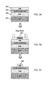
- FIGS. 6 and 7 depict aspects of additional alternative embodiments of a semiconductor device structure for selective etching of III-nitride and related materials in accordance with one or more aspects of the present invention, in which the structure includes multiple or repeating Sc-containing etch-stop layers.
- a semiconductor device structure in accordance with the present invention can include one or more repeating series of alternating Sc-containing etch-stop layers 603 a / 603 b and intermediate epitaxial layers 602 a / 602 b .
- Such a structure can allow multiple dry etches at different stages of the process, using any suitable etching scheme such as a timed dry etch or a wet etch to etch through the upper Sc-containing etch-stop layer 603 b prior to a second etch. This second etch would then proceed though the upper intermediate epitaxial layers 602 b and use the lower Sc-containing etch-stop layer 603 b to control the second etch depth.
- This method would work particularly well in cases where precise etching of two separate device layers is required to maximize device performance.
- the overlying layers 704 can contain any combination of epitaxial and non-epitaxial layers. Following the transfer, the device structure can be flipped over and mounted to a carrier 720 . The optional intermediate epitaxial layers 702 can then be etched in a top-down manner making use of the Sc-containing etch-stop layer 703 . Such a process may be used, for example, to controllably remove a defective (AlN and/or AlN/GaN) buffer layer while protecting device layers (which are included in the overlaying layers 704 in this example).
- the Sc-containing etch-stop layer comprises a high-fraction Sc x Al 1-x N, with x ⁇ 0.57, in conjunction with cubic semiconductors, such as cubic (In,Ga,Al)N, having a lattice constant similar to that of the etch-stop layer.
- cubic semiconductors such as cubic (In,Ga,Al)N
- x ⁇ 0.57 Sc x Al 1-x N is stable in a rock salt crystal structure and more compatible with cubic III-N materials, or other cubic materials.
- the higher Sc composition should also improve the selectivity with respect to Al x Ga 1-x N. See S. Zhang et al., “Tunable optoelectronic and ferroelectric properties in Sc-based III-nitrides,” J. Appl. Phys. 114, 133510 (2013).
- the primary advantage of the current method is improved dry etch selectivity of a AlN or high Al-fraction AlGaN or InAlN layer with respect to existing epitaxial etch-stop layers.
- the current method is stable over the commonly used range of temperatures and uses widely available standard etch chemistries and conditions.
- the prior art makes use of either Al-containing etch-stop layers, which cannot be etched selectively with respect to AlN or higher Al fraction Al x Ga 1-x N (see Buttari, supra; Lee, supra; and Pearton, supra), or In-containing etch-stop layer, which only function for low temperatures and low etch powers. See Pearton, supra.
- Sc x Al 1-x N etch-stop layers can be grown lattice-matched to GaN for x ⁇ 0.2, see Moram 2014, supra, which avoids etch-stop layer thickness constraints and greatly simplifies integration of ScAlN with GaN-based devices.
- InGaN and AlGaN etch-stop layer cannot be lattice-matched to GaN.
- the etch-stop can also contain a low alloy fraction of Sc, allowing for the ScAlN film to be grown sufficiently thick on AlN.
Landscapes
- Drying Of Semiconductors (AREA)
- Junction Field-Effect Transistors (AREA)
- Physics & Mathematics (AREA)
- Engineering & Computer Science (AREA)
- Plasma & Fusion (AREA)
- Led Devices (AREA)
Priority Applications (1)
| Application Number | Priority Date | Filing Date | Title |
|---|---|---|---|
| US15/807,821 US10283597B2 (en) | 2016-11-10 | 2017-11-09 | Scandium-containing III-N etch-stop layers for selective etching of III-nitrides and related materials |
Applications Claiming Priority (2)
| Application Number | Priority Date | Filing Date | Title |
|---|---|---|---|
| US201662420029P | 2016-11-10 | 2016-11-10 | |
| US15/807,821 US10283597B2 (en) | 2016-11-10 | 2017-11-09 | Scandium-containing III-N etch-stop layers for selective etching of III-nitrides and related materials |
Publications (2)
| Publication Number | Publication Date |
|---|---|
| US20180130883A1 US20180130883A1 (en) | 2018-05-10 |
| US10283597B2 true US10283597B2 (en) | 2019-05-07 |
Family
ID=62064480
Family Applications (1)
| Application Number | Title | Priority Date | Filing Date |
|---|---|---|---|
| US15/807,821 Active US10283597B2 (en) | 2016-11-10 | 2017-11-09 | Scandium-containing III-N etch-stop layers for selective etching of III-nitrides and related materials |
Country Status (3)
| Country | Link |
|---|---|
| US (1) | US10283597B2 (de) |
| EP (1) | EP3539155A4 (de) |
| WO (1) | WO2018089579A2 (de) |
Cited By (3)
| Publication number | Priority date | Publication date | Assignee | Title |
|---|---|---|---|---|
| US11848662B2 (en) | 2020-09-11 | 2023-12-19 | Raytheon Company | Tunable monolithic group III-nitride filter banks |
| EP4334514A4 (de) * | 2021-05-07 | 2025-03-19 | The Regents Of The University Of Michigan | Ferroelektronik aus epitaktischem nitrid |
| US12557321B2 (en) | 2021-02-12 | 2026-02-17 | Raytheon Company | Rare-earth III-nitride N-polar HEMT |
Families Citing this family (20)
| Publication number | Priority date | Publication date | Assignee | Title |
|---|---|---|---|---|
| US10355014B1 (en) * | 2017-12-22 | 2019-07-16 | Micron Technology, Inc. | Assemblies having vertically-extending structures |
| US11262604B2 (en) * | 2018-05-11 | 2022-03-01 | Raytheon Bbn Technologies Corp. | Photonic devices |
| US11054673B2 (en) | 2018-05-11 | 2021-07-06 | Raytheon Bbn Technologies Corp. | Photonic devices |
| KR102634586B1 (ko) * | 2018-06-11 | 2024-02-07 | 삼성디스플레이 주식회사 | 발광 소자, 그 제조방법 및 발광 소자를 포함하는 표시 장치 |
| CN108615756B (zh) * | 2018-06-15 | 2024-06-14 | 苏州汉骅半导体有限公司 | 半导体器件 |
| US10651048B1 (en) * | 2018-08-28 | 2020-05-12 | National Technology & Engineering Solutions Of Sandia, Llc | ScAIN etch mask for highly selective etching |
| CN111653617B (zh) * | 2020-03-31 | 2022-09-09 | 厦门市三安集成电路有限公司 | 一种增强型氮化物功率器件及制作方法 |
| WO2021225426A1 (ko) * | 2020-05-08 | 2021-11-11 | An Sang Jeong | 압전 박막을 제조하는 방법 및 이 박막을 이용하는 소자 |
| KR102457270B1 (ko) * | 2020-05-08 | 2022-10-21 | 웨이브로드 주식회사 | 압전 박막을 제조하는 방법 및 이 박막을 이용하는 소자 |
| FR3110283B1 (fr) * | 2020-05-18 | 2022-04-15 | Soitec Silicon On Insulator | Procédé de fabrication d’un substrat semi-conducteur sur isolant pour applications radiofréquences |
| US20220122837A1 (en) * | 2020-10-21 | 2022-04-21 | University Of South Carolina | Approach for Fabricating N-Polar AlxGa1-xN Devices |
| CN112531460B (zh) * | 2020-12-07 | 2021-11-02 | 全磊光电股份有限公司 | 一种高温工作的dfb激光器及外延结构生长方法 |
| US11942919B2 (en) | 2021-01-11 | 2024-03-26 | Raytheon Company | Strain compensated rare earth group III-nitride heterostructures |
| WO2023167709A2 (en) * | 2021-08-24 | 2023-09-07 | The Regents Of The University Of Michigan | Semiconductor heterostructures with scandium iii-nitride layer |
| WO2023214993A2 (en) * | 2021-10-22 | 2023-11-09 | The Regents Of The University Of Michigan | Semiconductor heterostructures with quaternary iii-nitride alloy |
| GB202117193D0 (en) * | 2021-11-29 | 2022-01-12 | Spts Technologies Ltd | A method of plasma etching |
| EP4199687B1 (de) * | 2021-12-17 | 2024-04-10 | SPTS Technologies Limited | Plasmaätzen von additive enthaltendem aln |
| EP4552444A2 (de) * | 2022-07-07 | 2025-05-14 | The Regents Of The University Of Michigan | Ferroelektrische iii-nitrid heterostrukturen |
| WO2024096966A1 (en) * | 2022-09-20 | 2024-05-10 | The Regents Of The University Of Michigan | Heterostructures with ferroelectric iii-nitride layer on metal |
| GB202219567D0 (en) * | 2022-12-22 | 2023-02-08 | Spts Technologies Ltd | Method of plasma etching |
Citations (16)
| Publication number | Priority date | Publication date | Assignee | Title |
|---|---|---|---|---|
| US20090029555A1 (en) | 2007-07-26 | 2009-01-29 | Unity Semiconductor Corporation | Multi-Step selective etching for cross-point memory |
| WO2010013821A1 (en) | 2008-07-28 | 2010-02-04 | Canon Kabushiki Kaisha | Method of producing optical element and optical element |
| US20120061683A1 (en) | 2009-03-27 | 2012-03-15 | Dowa Electronics Materials Co., Ltd. | Group iii nitride semiconductor growth substrate, group iii nitride semiconductor epitaxial substrate, group iii nitride semiconductor element and group iii nitride semiconductor free-standing substrate, and method of producing the same |
| US20130084441A1 (en) | 2011-09-29 | 2013-04-04 | Seagate Technology Llc | Optical articles and methods of making same |
| US20130279102A1 (en) * | 2011-11-03 | 2013-10-24 | Ruth A. Brain | Etchstop layers and capacitors |
| US8901708B2 (en) * | 2008-04-23 | 2014-12-02 | Intermolecular, Inc. | Yttrium and titanium high-k dielectric films |
| US20150021624A1 (en) | 2013-07-16 | 2015-01-22 | David J. Meyer | Lift-off of epitaxial layers from silicon carbide or compound semiconductor substrates |
| US20150140710A1 (en) | 2013-10-18 | 2015-05-21 | Soraa Laser Diode, Inc. | Manufacturable laser diode formed on c-plane gallium and nitrogen material |
| US9147726B2 (en) * | 2013-03-12 | 2015-09-29 | Siltronic Ag | Semiconductor wafer with a layer of AlzGa1-zN and process for producing it |
| US20170198410A1 (en) * | 2011-07-25 | 2017-07-13 | Toshiba Corporation | Nucleation of aluminum nitride on a silicon substrate using an ammonia preflow |
| US20170213732A1 (en) * | 2016-01-26 | 2017-07-27 | Asm Ip Holding B.V. | Semiconductor device fabrication using etch stop layer |
| US20170294529A1 (en) * | 2016-04-11 | 2017-10-12 | Qorvo Us, Inc. | High electron mobility transistor (hemt) device |
| US20170338101A1 (en) * | 2016-05-20 | 2017-11-23 | Panasonic Corporation | Group iii nitride semiconductor, and method for producing same |
| US20180138303A1 (en) * | 2016-11-11 | 2018-05-17 | Robert L. Coffie | Transistor structure including a scandium gallium nitride back-barrier layer |
| US20190036592A1 (en) * | 2016-03-11 | 2019-01-31 | Akoustis, Inc. | FRONT END MODULE FOR 5.2 GHz Wi-Fi ACOUSTIC WAVE RESONATOR RF FILTER CIRCUIT |
| US10217930B1 (en) * | 2016-03-11 | 2019-02-26 | Akoustis, Inc. | Method of manufacture for single crystal acoustic resonator devices using micro-vias |
Family Cites Families (2)
| Publication number | Priority date | Publication date | Assignee | Title |
|---|---|---|---|---|
| JP4531071B2 (ja) * | 2007-02-20 | 2010-08-25 | 富士通株式会社 | 化合物半導体装置 |
| FR2929445B1 (fr) * | 2008-03-25 | 2010-05-21 | Picogiga Internat | Procede de fabrication d'une couche de nitrure de gallium ou de nitrure de gallium et d'aluminium |
-
2017
- 2017-11-09 EP EP17870039.9A patent/EP3539155A4/de not_active Withdrawn
- 2017-11-09 WO PCT/US2017/060771 patent/WO2018089579A2/en not_active Ceased
- 2017-11-09 US US15/807,821 patent/US10283597B2/en active Active
Patent Citations (16)
| Publication number | Priority date | Publication date | Assignee | Title |
|---|---|---|---|---|
| US20090029555A1 (en) | 2007-07-26 | 2009-01-29 | Unity Semiconductor Corporation | Multi-Step selective etching for cross-point memory |
| US8901708B2 (en) * | 2008-04-23 | 2014-12-02 | Intermolecular, Inc. | Yttrium and titanium high-k dielectric films |
| WO2010013821A1 (en) | 2008-07-28 | 2010-02-04 | Canon Kabushiki Kaisha | Method of producing optical element and optical element |
| US20120061683A1 (en) | 2009-03-27 | 2012-03-15 | Dowa Electronics Materials Co., Ltd. | Group iii nitride semiconductor growth substrate, group iii nitride semiconductor epitaxial substrate, group iii nitride semiconductor element and group iii nitride semiconductor free-standing substrate, and method of producing the same |
| US20170198410A1 (en) * | 2011-07-25 | 2017-07-13 | Toshiba Corporation | Nucleation of aluminum nitride on a silicon substrate using an ammonia preflow |
| US20130084441A1 (en) | 2011-09-29 | 2013-04-04 | Seagate Technology Llc | Optical articles and methods of making same |
| US20130279102A1 (en) * | 2011-11-03 | 2013-10-24 | Ruth A. Brain | Etchstop layers and capacitors |
| US9147726B2 (en) * | 2013-03-12 | 2015-09-29 | Siltronic Ag | Semiconductor wafer with a layer of AlzGa1-zN and process for producing it |
| US20150021624A1 (en) | 2013-07-16 | 2015-01-22 | David J. Meyer | Lift-off of epitaxial layers from silicon carbide or compound semiconductor substrates |
| US20150140710A1 (en) | 2013-10-18 | 2015-05-21 | Soraa Laser Diode, Inc. | Manufacturable laser diode formed on c-plane gallium and nitrogen material |
| US20170213732A1 (en) * | 2016-01-26 | 2017-07-27 | Asm Ip Holding B.V. | Semiconductor device fabrication using etch stop layer |
| US20190036592A1 (en) * | 2016-03-11 | 2019-01-31 | Akoustis, Inc. | FRONT END MODULE FOR 5.2 GHz Wi-Fi ACOUSTIC WAVE RESONATOR RF FILTER CIRCUIT |
| US10217930B1 (en) * | 2016-03-11 | 2019-02-26 | Akoustis, Inc. | Method of manufacture for single crystal acoustic resonator devices using micro-vias |
| US20170294529A1 (en) * | 2016-04-11 | 2017-10-12 | Qorvo Us, Inc. | High electron mobility transistor (hemt) device |
| US20170338101A1 (en) * | 2016-05-20 | 2017-11-23 | Panasonic Corporation | Group iii nitride semiconductor, and method for producing same |
| US20180138303A1 (en) * | 2016-11-11 | 2018-05-17 | Robert L. Coffie | Transistor structure including a scandium gallium nitride back-barrier layer |
Non-Patent Citations (21)
| Title |
|---|
| A. Konno et al., "Thin Film from Bulk and Leaky Lamb Waves in MEMS-based Samples," 2014 IEEE International Ultrasonics Symposium Proceedings, pp. 273-276. |
| C. L. Yaws, The Yaws Handbook of Vapor Pressure: Antoine coefficients, 2nd ed. Waltham, MA, USA: Gulf Professional Publishing, 2015, pp. 316-320. |
| D. Buttari, et al., "Selective Dry Etching of GaN Over AlGaN in BCl3/SF6 Mixtures," International Journal of High Speed Electronics and Systems, vol. 14, pp. 756 761, 2004. |
| G. H. Rinehart et al., "Vapor Pressure and Vaporization Thermodynamics of Scandium Trifluoride," J. Less Common Met., vol. 75, pp. 65 78, 1980. |
| G. Piazza, et al., "Piezoelectric aluminum nitride thin films for microelectromechanical systems," MRS Bulletin, vol. 37, pp. 1051 1061, Nov. 2012. |
| Hardy ey. al., "Epitaxial ScAlN etch stop Layers Grown by Molecular Beam Epitaxy for Selective Etching of AlN and GaN," IEEE Transactions on Semiconductor Manufacturing, vol. 30, No. 4, Nov. 2017. * |
| Henry et. al., "ScAlN etch mask for highly selective silicon etching", J. Vac. Sci. Technol. B 35(5), Sep./Oct. 2017 (Year: 2017). * |
| J. M. Lee, et al., "Highly selective dry etching of III nitrides using an inductively coupled Cl2/Ar/O2 plasma," J. Vac. Sci. Technol., B, vol. 18, pp. 1409 1411, 2000. |
| Lee et. al., "Bendable GaN high electron mobility transistors on plastic substrates," Journal of Applied Physics 100, 124507 (2006) ("Lee"). * |
| M. A. Moram et al., "ScGaN and ScAlN: emerging nitride materials," J. Mater. Chem. A, vol. 2, pp. 6042 6050, 2014. |
| M. A. Moram, et al., "The effect of oxygen incorporation in sputtered scandium nitride films," Thin Solid Films, vol. 516, pp. 8569 8572, 2008. |
| M. Akiyama, et al., "Enhancement of Piezoelectric Response in Scandium Aluminum Nitride Alloy Thin Films Prepared by Dual Reactive Cosputtering," Adv. Mater., vol. 21, pp. 593 596, 2009. |
| M. T. Hardy, et al., "Epitaxial ScAlN grown by molecular beam epitaxy on GaN and SiC substrates," App. Phys. Lett. 110, 162104 (2017). |
| Moram et. al., "Structural properties of wurzitelike ScGaN films grown by NH3-molecular beam epitaxy," Journal of Applied Physics 106 113533 (2009). * |
| N. Sedrine et al., "Bandgap Engineering and Optical Constants of YxAl1-xN Alloys," Japanese Journal of Applied Physics 52 (2013) 08JM02. |
| S. J. Pearton, et al., "A Review of Dry Etching of GaN and Related Materials," MRS Internet J. Nitride Semicond. Res., 5, 11, pp. 1-38 (2000). |
| S. M. Knoll, et al., "Defects in epitaxial ScGaN: Dislocations, stacking faults, and cubic inclusions," Appl. Phys. Lett. 104, 101906 (2014). |
| S. Sergent, et al., "High Q AlN photonic crystal nanobeam cavities fabricated by layer transfer," Appl. Phys. Lett., vol. 101, p. 101106, 2012. |
| S. Zhang et al., "Tunable optoelectronic and ferroelectric properties in Sc based III nitrides," J. Appl. Phys. 114, 133510 (2013). |
| Search Report and Written Opinion dated Feb. 27, 2018 in corresponding International Application No. PCT/US17/60771. |
| Tsui, "Characterisation of scandium-based III-nitride thin films," Department of Materials, Imperial College London, Thesis, Doctor of Philosophy, Mar. 2016. * |
Cited By (3)
| Publication number | Priority date | Publication date | Assignee | Title |
|---|---|---|---|---|
| US11848662B2 (en) | 2020-09-11 | 2023-12-19 | Raytheon Company | Tunable monolithic group III-nitride filter banks |
| US12557321B2 (en) | 2021-02-12 | 2026-02-17 | Raytheon Company | Rare-earth III-nitride N-polar HEMT |
| EP4334514A4 (de) * | 2021-05-07 | 2025-03-19 | The Regents Of The University Of Michigan | Ferroelektronik aus epitaktischem nitrid |
Also Published As
| Publication number | Publication date |
|---|---|
| US20180130883A1 (en) | 2018-05-10 |
| EP3539155A4 (de) | 2020-06-17 |
| WO2018089579A2 (en) | 2018-05-17 |
| EP3539155A2 (de) | 2019-09-18 |
| WO2018089579A3 (en) | 2018-07-26 |
Similar Documents
| Publication | Publication Date | Title |
|---|---|---|
| US10283597B2 (en) | Scandium-containing III-N etch-stop layers for selective etching of III-nitrides and related materials | |
| US9876081B2 (en) | Lift-off of epitaxial layers from silicon carbide or compound semiconductor substrates | |
| US8048225B2 (en) | Large-area bulk gallium nitride wafer and method of manufacture | |
| US10192737B2 (en) | Method for heteroepitaxial growth of III metal-face polarity III-nitrides on substrates with diamond crystal structure and III-nitride semiconductors | |
| US8878252B2 (en) | III-V compound semiconductor epitaxy from a non-III-V substrate | |
| JP5328931B2 (ja) | 低欠陥密度の自立窒化ガリウム基板の製法およびそれにより製造されたデバイス | |
| Guo et al. | Comparative study of etching high crystalline quality AlN and GaN | |
| Hardy et al. | Epitaxial ScAlN etch-stop layers grown by molecular beam epitaxy for selective etching of AlN and GaN | |
| US8803189B2 (en) | III-V compound semiconductor epitaxy using lateral overgrowth | |
| JP5317398B2 (ja) | 格子パラメータを変化させる元素を含有する窒化ガリウムデバイス基板 | |
| US8629065B2 (en) | Growth of planar non-polar {10-10} M-plane gallium nitride with hydride vapor phase epitaxy (HVPE) | |
| US10158046B2 (en) | Semiconductor element and fabrication method thereof | |
| US20100035416A1 (en) | Forming III-Nitride Semiconductor Wafers Using Nano-Structures | |
| US20130099277A1 (en) | SELECTIVE DRY ETCHING OF N-FACE (Al,In,Ga)N HETEROSTRUCTURES | |
| JP5371430B2 (ja) | 半導体基板並びにハイドライド気相成長法により自立半導体基板を製造するための方法及びそれに使用されるマスク層 | |
| US11342477B2 (en) | III-nitride semiconductor devices | |
| US20140246679A1 (en) | III-N MATERIAL GROWN ON ErAlN BUFFER ON Si SUBSTRATE | |
| US10553426B2 (en) | Method for obtaining a semi-polar nitride layer on a crystalline substrate | |
| US8143630B2 (en) | Zinc sulfide substrates for group III-nitride epitaxy and group III-nitride devices | |
| TWI875852B (zh) | 積層膜結構體、半導體元件、電子設備、及積層膜結構體的製造方法 | |
| JP2008074671A (ja) | 自立窒化物基板の製造方法 | |
| JP5225133B2 (ja) | GaN系化合物半導体の成長方法及び成長層付き基板 | |
| US20130214282A1 (en) | Iii-n on silicon using nano structured interface layer | |
| JP2016533643A (ja) | 半導体ウェハおよび半導体ウェハを製造するための方法 | |
| KR101686677B1 (ko) | 반도체 박막 성장 방법 및 이에 의해 성장된 반도체의 박막 |
Legal Events
| Date | Code | Title | Description |
|---|---|---|---|
| AS | Assignment |
Owner name: THE GOVERNMENT OF THE UNITED STATES OF AMERICA, AS Free format text: ASSIGNMENT OF ASSIGNORS INTEREST;ASSIGNORS:HARDY, MATTHEW T.;DOWNEY, BRIAN P.;MEYER, DAVID J.;SIGNING DATES FROM 20171106 TO 20171107;REEL/FRAME:044080/0163 |
|
| FEPP | Fee payment procedure |
Free format text: ENTITY STATUS SET TO UNDISCOUNTED (ORIGINAL EVENT CODE: BIG.); ENTITY STATUS OF PATENT OWNER: LARGE ENTITY |
|
| STPP | Information on status: patent application and granting procedure in general |
Free format text: PUBLICATIONS -- ISSUE FEE PAYMENT VERIFIED |
|
| STCF | Information on status: patent grant |
Free format text: PATENTED CASE |
|
| MAFP | Maintenance fee payment |
Free format text: PAYMENT OF MAINTENANCE FEE, 4TH YEAR, LARGE ENTITY (ORIGINAL EVENT CODE: M1551); ENTITY STATUS OF PATENT OWNER: LARGE ENTITY Year of fee payment: 4 |