US10310306B2 - Liquid crystal display panel and apparatus - Google Patents
Liquid crystal display panel and apparatus Download PDFInfo
- Publication number
- US10310306B2 US10310306B2 US15/572,821 US201715572821A US10310306B2 US 10310306 B2 US10310306 B2 US 10310306B2 US 201715572821 A US201715572821 A US 201715572821A US 10310306 B2 US10310306 B2 US 10310306B2
- Authority
- US
- United States
- Prior art keywords
- pixel unit
- region
- liquid crystal
- crystal display
- thin film
- Prior art date
- Legal status (The legal status is an assumption and is not a legal conclusion. Google has not performed a legal analysis and makes no representation as to the accuracy of the status listed.)
- Active
Links
Images


Classifications
-
- G—PHYSICS
- G02—OPTICS
- G02F—OPTICAL DEVICES OR ARRANGEMENTS FOR THE CONTROL OF LIGHT BY MODIFICATION OF THE OPTICAL PROPERTIES OF THE MEDIA OF THE ELEMENTS INVOLVED THEREIN; NON-LINEAR OPTICS; FREQUENCY-CHANGING OF LIGHT; OPTICAL LOGIC ELEMENTS; OPTICAL ANALOGUE/DIGITAL CONVERTERS
- G02F1/00—Devices or arrangements for the control of the intensity, colour, phase, polarisation or direction of light arriving from an independent light source, e.g. switching, gating or modulating; Non-linear optics
- G02F1/01—Devices or arrangements for the control of the intensity, colour, phase, polarisation or direction of light arriving from an independent light source, e.g. switching, gating or modulating; Non-linear optics for the control of the intensity, phase, polarisation or colour
- G02F1/13—Devices or arrangements for the control of the intensity, colour, phase, polarisation or direction of light arriving from an independent light source, e.g. switching, gating or modulating; Non-linear optics for the control of the intensity, phase, polarisation or colour based on liquid crystals, e.g. single liquid crystal display cells
- G02F1/133—Constructional arrangements; Operation of liquid crystal cells; Circuit arrangements
- G02F1/13306—Circuit arrangements or driving methods for the control of single liquid crystal cells
-
- G—PHYSICS
- G02—OPTICS
- G02F—OPTICAL DEVICES OR ARRANGEMENTS FOR THE CONTROL OF LIGHT BY MODIFICATION OF THE OPTICAL PROPERTIES OF THE MEDIA OF THE ELEMENTS INVOLVED THEREIN; NON-LINEAR OPTICS; FREQUENCY-CHANGING OF LIGHT; OPTICAL LOGIC ELEMENTS; OPTICAL ANALOGUE/DIGITAL CONVERTERS
- G02F1/00—Devices or arrangements for the control of the intensity, colour, phase, polarisation or direction of light arriving from an independent light source, e.g. switching, gating or modulating; Non-linear optics
- G02F1/01—Devices or arrangements for the control of the intensity, colour, phase, polarisation or direction of light arriving from an independent light source, e.g. switching, gating or modulating; Non-linear optics for the control of the intensity, phase, polarisation or colour
- G02F1/13—Devices or arrangements for the control of the intensity, colour, phase, polarisation or direction of light arriving from an independent light source, e.g. switching, gating or modulating; Non-linear optics for the control of the intensity, phase, polarisation or colour based on liquid crystals, e.g. single liquid crystal display cells
- G02F1/133—Constructional arrangements; Operation of liquid crystal cells; Circuit arrangements
- G02F1/136—Liquid crystal cells structurally associated with a semi-conducting layer or substrate, e.g. cells forming part of an integrated circuit
- G02F1/1362—Active matrix addressed cells
-
- G—PHYSICS
- G02—OPTICS
- G02F—OPTICAL DEVICES OR ARRANGEMENTS FOR THE CONTROL OF LIGHT BY MODIFICATION OF THE OPTICAL PROPERTIES OF THE MEDIA OF THE ELEMENTS INVOLVED THEREIN; NON-LINEAR OPTICS; FREQUENCY-CHANGING OF LIGHT; OPTICAL LOGIC ELEMENTS; OPTICAL ANALOGUE/DIGITAL CONVERTERS
- G02F1/00—Devices or arrangements for the control of the intensity, colour, phase, polarisation or direction of light arriving from an independent light source, e.g. switching, gating or modulating; Non-linear optics
- G02F1/01—Devices or arrangements for the control of the intensity, colour, phase, polarisation or direction of light arriving from an independent light source, e.g. switching, gating or modulating; Non-linear optics for the control of the intensity, phase, polarisation or colour
- G02F1/13—Devices or arrangements for the control of the intensity, colour, phase, polarisation or direction of light arriving from an independent light source, e.g. switching, gating or modulating; Non-linear optics for the control of the intensity, phase, polarisation or colour based on liquid crystals, e.g. single liquid crystal display cells
- G02F1/133—Constructional arrangements; Operation of liquid crystal cells; Circuit arrangements
- G02F1/136—Liquid crystal cells structurally associated with a semi-conducting layer or substrate, e.g. cells forming part of an integrated circuit
- G02F1/1362—Active matrix addressed cells
- G02F1/136213—Storage capacitors associated with the pixel electrode
-
- G—PHYSICS
- G02—OPTICS
- G02F—OPTICAL DEVICES OR ARRANGEMENTS FOR THE CONTROL OF LIGHT BY MODIFICATION OF THE OPTICAL PROPERTIES OF THE MEDIA OF THE ELEMENTS INVOLVED THEREIN; NON-LINEAR OPTICS; FREQUENCY-CHANGING OF LIGHT; OPTICAL LOGIC ELEMENTS; OPTICAL ANALOGUE/DIGITAL CONVERTERS
- G02F1/00—Devices or arrangements for the control of the intensity, colour, phase, polarisation or direction of light arriving from an independent light source, e.g. switching, gating or modulating; Non-linear optics
- G02F1/01—Devices or arrangements for the control of the intensity, colour, phase, polarisation or direction of light arriving from an independent light source, e.g. switching, gating or modulating; Non-linear optics for the control of the intensity, phase, polarisation or colour
- G02F1/13—Devices or arrangements for the control of the intensity, colour, phase, polarisation or direction of light arriving from an independent light source, e.g. switching, gating or modulating; Non-linear optics for the control of the intensity, phase, polarisation or colour based on liquid crystals, e.g. single liquid crystal display cells
- G02F1/133—Constructional arrangements; Operation of liquid crystal cells; Circuit arrangements
- G02F1/136—Liquid crystal cells structurally associated with a semi-conducting layer or substrate, e.g. cells forming part of an integrated circuit
- G02F1/1362—Active matrix addressed cells
- G02F1/13624—Active matrix addressed cells having more than one switching element per pixel
-
- G—PHYSICS
- G02—OPTICS
- G02F—OPTICAL DEVICES OR ARRANGEMENTS FOR THE CONTROL OF LIGHT BY MODIFICATION OF THE OPTICAL PROPERTIES OF THE MEDIA OF THE ELEMENTS INVOLVED THEREIN; NON-LINEAR OPTICS; FREQUENCY-CHANGING OF LIGHT; OPTICAL LOGIC ELEMENTS; OPTICAL ANALOGUE/DIGITAL CONVERTERS
- G02F1/00—Devices or arrangements for the control of the intensity, colour, phase, polarisation or direction of light arriving from an independent light source, e.g. switching, gating or modulating; Non-linear optics
- G02F1/01—Devices or arrangements for the control of the intensity, colour, phase, polarisation or direction of light arriving from an independent light source, e.g. switching, gating or modulating; Non-linear optics for the control of the intensity, phase, polarisation or colour
- G02F1/13—Devices or arrangements for the control of the intensity, colour, phase, polarisation or direction of light arriving from an independent light source, e.g. switching, gating or modulating; Non-linear optics for the control of the intensity, phase, polarisation or colour based on liquid crystals, e.g. single liquid crystal display cells
- G02F1/133—Constructional arrangements; Operation of liquid crystal cells; Circuit arrangements
- G02F1/136—Liquid crystal cells structurally associated with a semi-conducting layer or substrate, e.g. cells forming part of an integrated circuit
- G02F1/1362—Active matrix addressed cells
- G02F1/136286—Wiring, e.g. gate line, drain line
-
- G—PHYSICS
- G09—EDUCATION; CRYPTOGRAPHY; DISPLAY; ADVERTISING; SEALS
- G09G—ARRANGEMENTS OR CIRCUITS FOR CONTROL OF INDICATING DEVICES USING STATIC MEANS TO PRESENT VARIABLE INFORMATION
- G09G3/00—Control arrangements or circuits, of interest only in connection with visual indicators other than cathode-ray tubes
- G09G3/20—Control arrangements or circuits, of interest only in connection with visual indicators other than cathode-ray tubes for presentation of an assembly of a number of characters, e.g. a page, by composing the assembly by combination of individual elements arranged in a matrix no fixed position being assigned to or needed to be assigned to the individual characters or partial characters
- G09G3/34—Control arrangements or circuits, of interest only in connection with visual indicators other than cathode-ray tubes for presentation of an assembly of a number of characters, e.g. a page, by composing the assembly by combination of individual elements arranged in a matrix no fixed position being assigned to or needed to be assigned to the individual characters or partial characters by control of light from an independent source
- G09G3/36—Control arrangements or circuits, of interest only in connection with visual indicators other than cathode-ray tubes for presentation of an assembly of a number of characters, e.g. a page, by composing the assembly by combination of individual elements arranged in a matrix no fixed position being assigned to or needed to be assigned to the individual characters or partial characters by control of light from an independent source using liquid crystals
- G09G3/3607—Control arrangements or circuits, of interest only in connection with visual indicators other than cathode-ray tubes for presentation of an assembly of a number of characters, e.g. a page, by composing the assembly by combination of individual elements arranged in a matrix no fixed position being assigned to or needed to be assigned to the individual characters or partial characters by control of light from an independent source using liquid crystals for displaying colours or for displaying grey scales with a specific pixel layout, e.g. using sub-pixels
-
- G—PHYSICS
- G09—EDUCATION; CRYPTOGRAPHY; DISPLAY; ADVERTISING; SEALS
- G09G—ARRANGEMENTS OR CIRCUITS FOR CONTROL OF INDICATING DEVICES USING STATIC MEANS TO PRESENT VARIABLE INFORMATION
- G09G3/00—Control arrangements or circuits, of interest only in connection with visual indicators other than cathode-ray tubes
- G09G3/20—Control arrangements or circuits, of interest only in connection with visual indicators other than cathode-ray tubes for presentation of an assembly of a number of characters, e.g. a page, by composing the assembly by combination of individual elements arranged in a matrix no fixed position being assigned to or needed to be assigned to the individual characters or partial characters
- G09G3/34—Control arrangements or circuits, of interest only in connection with visual indicators other than cathode-ray tubes for presentation of an assembly of a number of characters, e.g. a page, by composing the assembly by combination of individual elements arranged in a matrix no fixed position being assigned to or needed to be assigned to the individual characters or partial characters by control of light from an independent source
- G09G3/36—Control arrangements or circuits, of interest only in connection with visual indicators other than cathode-ray tubes for presentation of an assembly of a number of characters, e.g. a page, by composing the assembly by combination of individual elements arranged in a matrix no fixed position being assigned to or needed to be assigned to the individual characters or partial characters by control of light from an independent source using liquid crystals
- G09G3/3611—Control of matrices with row and column drivers
- G09G3/3648—Control of matrices with row and column drivers using an active matrix
-
- G—PHYSICS
- G02—OPTICS
- G02F—OPTICAL DEVICES OR ARRANGEMENTS FOR THE CONTROL OF LIGHT BY MODIFICATION OF THE OPTICAL PROPERTIES OF THE MEDIA OF THE ELEMENTS INVOLVED THEREIN; NON-LINEAR OPTICS; FREQUENCY-CHANGING OF LIGHT; OPTICAL LOGIC ELEMENTS; OPTICAL ANALOGUE/DIGITAL CONVERTERS
- G02F2201/00—Constructional arrangements not provided for in groups G02F1/00 - G02F7/00
- G02F2201/12—Constructional arrangements not provided for in groups G02F1/00 - G02F7/00 electrode
- G02F2201/121—Constructional arrangements not provided for in groups G02F1/00 - G02F7/00 electrode common or background
-
- G—PHYSICS
- G09—EDUCATION; CRYPTOGRAPHY; DISPLAY; ADVERTISING; SEALS
- G09G—ARRANGEMENTS OR CIRCUITS FOR CONTROL OF INDICATING DEVICES USING STATIC MEANS TO PRESENT VARIABLE INFORMATION
- G09G2300/00—Aspects of the constitution of display devices
- G09G2300/08—Active matrix structure, i.e. with use of active elements, inclusive of non-linear two terminal elements, in the pixels together with light emitting or modulating elements
- G09G2300/0809—Several active elements per pixel in active matrix panels
- G09G2300/0842—Several active elements per pixel in active matrix panels forming a memory circuit, e.g. a dynamic memory with one capacitor
- G09G2300/0852—Several active elements per pixel in active matrix panels forming a memory circuit, e.g. a dynamic memory with one capacitor being a dynamic memory with more than one capacitor
-
- G—PHYSICS
- G09—EDUCATION; CRYPTOGRAPHY; DISPLAY; ADVERTISING; SEALS
- G09G—ARRANGEMENTS OR CIRCUITS FOR CONTROL OF INDICATING DEVICES USING STATIC MEANS TO PRESENT VARIABLE INFORMATION
- G09G2310/00—Command of the display device
- G09G2310/02—Addressing, scanning or driving the display screen or processing steps related thereto
- G09G2310/0243—Details of the generation of driving signals
- G09G2310/0251—Precharge or discharge of pixel before applying new pixel voltage
-
- G—PHYSICS
- G09—EDUCATION; CRYPTOGRAPHY; DISPLAY; ADVERTISING; SEALS
- G09G—ARRANGEMENTS OR CIRCUITS FOR CONTROL OF INDICATING DEVICES USING STATIC MEANS TO PRESENT VARIABLE INFORMATION
- G09G2320/00—Control of display operating conditions
- G09G2320/02—Improving the quality of display appearance
- G09G2320/028—Improving the quality of display appearance by changing the viewing angle properties, e.g. widening the viewing angle, adapting the viewing angle to the view direction
Definitions
- the present disclosure relates to the field of display technology, and more particularly to a liquid crystal display panel and an apparatus.
- LCD Liquid crystal displays
- TFT-LCDs thin film transistor LCDs
- CRT cathode ray tube
- MVA multi-domain vertical alignment
- IPS in plane switching
- each pixel units of present liquid crystal display panels include a main pixel area and a sub-pixel area.
- the main pixel area includes a first thin film transistor T 1 , a first storage capacitor Cst 1 , a first liquid crystal capacitor Clc 1 , a first capacitor C 1 , and a second capacitor C 2 .
- the sub-pixel area includes a second thin film transistor T 2 , a third thin film transistor T 3 , a second storage capacitor Cst 2 , and a second liquid crystal capacitor Clc 2 .
- the gate of the first thin film transistor T 1 and the gate of the second thin film transistor T 2 are both connected to a scan line Gn.
- the source of the first thin film transistor T 1 and the source of the second thin film transistor T 2 are connected to a data line Data.
- One side of both the first storage capacitor Cst 1 and the first liquid crystal capacitor Clc 1 are connected to a drain of the first thin film transistor T 1 .
- the other side of the first storage capacitor Cst 1 is connected to a common electrode disposed on the side of the array substrate.
- the other side of the first liquid crystal capacitor Clc 1 is connected to a common electrode disposed on the side of the color film substrate.
- One side of the first capacitor C 1 is connected to the drain of the first thin film transistor T 1
- the other side of the first capacitor C 1 is connected to the second capacitor C 2 .
- the other side of the second capacitor C 2 is connected to a common electrode of the array substrate.
- One side of both the second storage capacitor Cst 2 and the second liquid crystal capacitor Clc 2 are connected to a drain of the second thin film transistor T 2 .
- the other side of the second storage Cst 2 is connected to a common electrode of the array substrate; the other side of the second liquid crystal Clc 2 is connected to a common electrode of the color film substrate.
- the drain of the second thin film transistor T 2 is connected the source of the third thin film transistor T 3 .
- the drain of the third thin film transistor T 3 is connected to a node between the first capacitor and the second capacitor.
- the gate of the third thin film transistor T 3 is connected to scan line Gn+1.
- Va and Vb represent the voltage of a main pixel region and a sub-pixel region respectively.
- the signal of the scan line Gn is high, T 1 and T 2 are closed, T 3 is opened, Va and Vb are both at high potential.
- the scan line Gn is closed, the scan line Gn+1 is opened, T 1 and T 2 are opened, T 3 is closed, the second liquid crystal capacitor Clc 2 discharges in order to charge the lower-substrate of the first capacitor C 1 , the voltage of Va is increased, i.e., Va is higher than Vb, so that the viewing angle is increased.
- aperture ratio and the transmittance ratio will decrease since the number of the thin film transistors is higher.
- the object of this disclosure is providing a liquid crystal display panel and apparatus which can increase the aperture ratio.
- a liquid display panel which includes:
- a plurality of data lines, a plurality of scan lines, and a plurality of pixel sets comprising a first pixel unit and a second pixel unit; the scan lines being correspondingly connected to the pixel units arranged row by row, the data lines being correspondingly connected to the pixel units arranged column by column;
- the first pixel unit comprises a first thin film transistor, a first charging capacitor, a second charging capacitor, a first storage capacitor, and a first liquid crystal capacitor; a gate of the first thin film transistor is connected to a corresponding scan line, and a source of the first thin film transistor is connected to a corresponding data line; the first charging capacitance is connected between a drain of the first thin film transistor, and the second charging capacitor; the first storage capacitor and the first liquid crystal capacitor are connected to the drain of the first thin film transistor;
- the second pixel unit comprises a second thin film transistor, a second storage capacitor, and a second liquid crystal capacitor; a gate of the second thin film transistor is connected to a corresponding scan line, a source of the second thin film transistor is connected to a corresponding data line; a drain of the second thin film transistor is connected to the first charging capacitor, the second storage capacitor and the second liquid crystal capacitor are connected to the drain of the second thin film transistor; wherein a brightness of the first pixel unit is higher than a brightness of the second pixel unit.
- the first pixel unit and the second pixel unit are arranged in alternating rows.
- the first pixel unit and the second pixel unit are arranged alternately.
- the first pixel unit is disposed on an nth row and a (2k+1)th column or an (n+1)th row and a (2k)th column; the second pixel unit is disposed on an (n+1)th row and a (2k+1)th column or an nth row and a (2k)th column, where the liquid crystal display panel comprises n rows of pixel units, where 0 ⁇ n ⁇ N, N ⁇ 2, k ⁇ 0.
- the liquid crystal display panel comprises a first region and a second region, the first pixel unit of the first region is disposed on a same row with the second pixel unit of the second region; the second pixel unit of the first region is disposed on a same row with the first pixel unit of the second region.
- an area of the first region is equal to an area of the second region.
- the liquid crystal display panel comprises two first regions and a second region between the two first regions.
- a total area of the two first regions is equal to the area of the second region.
- liquid crystal display panel which includes:
- a plurality of data lines, a plurality of scan lines, and a plurality of pixel sets comprising a first pixel unit and a second pixel unit; the scan lines being correspondingly connected to the pixel units arranged row by row, the data lines being correspondingly connected to the pixel units arranged column by column;
- the first pixel unit comprises a first thin film transistor, a first charging capacitor, and a second charging capacitor; a gate of the first thin film transistor is connected to a corresponding scan line, and a source of the first thin film transistor is connected to a corresponding data line; the first charging capacitor is connected between a drain of the first thin film transistor, and the second charging capacitor;
- the second pixel unit comprises a second thin film transistor; a gate of the second thin film transistor is connected to a corresponding scan line, a source of the second thin film transistor is connected to a corresponding data line; a drain of the second thin film transistor is connected to the first charging capacitor.
- the first pixel unit and the second pixel unit are arranged in alternating rows.
- the first pixel unit and the second pixel unit are arranged alternately.
- the first pixel unit is disposed on an nth row and a (2k+1)th column or an (n+1) row and a (2k)th column; the second pixel unit is disposed on an (n+1)th row and a (2k+1)th column or an nth row and a (2k) column, where the liquid crystal display panel comprises n rows of pixel units, where 0 ⁇ n ⁇ N, N ⁇ 2, k ⁇ 0.
- the liquid crystal display panel comprises a first region and a second region, the first pixel unit of the first region is disposed on the same row with the second pixel unit of the second region; the second pixel unit of the first region is disposed on the same row with the first pixel unit of the second region;
- the first pixel unit of the first region is arranged in alternating rows with the second pixel unit of the first region; the first pixel unit of the second region is arranged in alternating rows with the second pixel unit of the second region.
- an area of the first region is equal to an area of the second region.
- the liquid crystal display panel comprises two first regions and a second region between the two first regions.
- a total area of the two first regions is equal to the area of the second region.
- the brightness of the first pixel unit is higher than a brightness of the second pixel unit.
- the present disclosure further provides a liquid crystal display apparatus includes a backlight module and any one of the abovementioned liquid crystal display panels.
- the liquid crystal display panel and apparatus of present disclosure keeps charging to the previous pixel unit while charging to the next pixel unit, in order to make the brightness of the adjacent pixel units different and increase the viewing angle of the liquid crystal display panel.
- the number of the thin film transistors and capacitors is decreased, thus the aperture ratio and transmittance ratio are increased.
- FIG. 1 illustrates a structural diagram of a present liquid crystal display panel.
- FIG. 2 illustrates waveforms of voltages applied on a main pixel unit and a sub-pixel unit in FIG. 1 .
- FIG. 3 illustrates a structural diagram of the liquid crystal display panel according to a first embodiment of the present disclosure.
- FIG. 4 illustrates a structural diagram of a pixel of the liquid crystal display panel in the present disclosure.
- FIG. 5 illustrates waveforms of the driving signals corresponding to FIG. 4 .
- FIG. 6 illustrates the diagram of the display brightness corresponding to FIG. 4 .
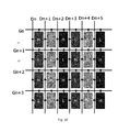
- FIG. 7 illustrates a structural diagram of the liquid crystal display panel according to a second embodiment of the present disclosure.
- FIG. 8 illustrates a diagram of the display brightness corresponding to FIG. 7 .
- FIG. 9 illustrates a structural diagram of the liquid crystal display panel according to a third embodiment of the present disclosure.
- FIG. 10 illustrates a diagram of the display brightness corresponding to FIG. 9 .
- FIG. 3 is a structural diagram of the liquid crystal display panel of present disclosure.
- the liquid crystal display panel of this embodiment includes a plurality of data lines Dn ⁇ Dn+5, a plurality of scan lines Gn ⁇ Gn+3, and a plurality of pixel sets 10 .
- Each of the pixel sets 10 includes two adjacent pixel units.
- the pixel units which are restricted by a plurality of scan lines are composed in plural rows.
- the pixel units which are restricted by a plurality of data lines are composed in a plurality of columns.
- Each one row of the pixel units is disposed with a scan line.
- Each one column of the pixel units is disposed with a data line.
- each of the pixel sets 10 includes a first pixel unit 11 and a second pixel unit 12 .
- the first pixel unit 11 includes a first thin film transistor T 1 , a first storage capacitor CST 1 , a first liquid crystal capacitor CLC 1 , a first charging capacitor CS 1 , and a second charging capacitor CS 2 .
- a gate of the first thin film transistor T 1 is connected to a corresponding scan line.
- a source of the first thin film transistor T 1 is connected to a corresponding data line.
- One side of both the first storage capacitor CST 1 and the first liquid crystal capacitor CLC 1 are connected to the drain of the first thin film transistor T 1 .
- the other side of the first storage capacitor CST 1 is connected to a common electrode on one side of the array substrate.
- the other side of the first liquid crystal capacitor CLC 1 is connected to a common electrode one side of the color film substrate.
- One side of the first charging capacitor CS 1 is connected to a drain of the first thin film transistor T 1 .
- the other side of the first charging capacitor CS 1 is connected to one side of the second charging capacitor CS 2 .
- the other side of the second charging capacitor is connected to the common electrode on the side of the array substrate.
- the second pixel unit includes a second thin film transistor T 2 , a second storage capacitor CST 2 , and a second liquid crystal capacitor CLC 2 .
- the gate of the second thin film transistor T 2 is connected to a corresponding scan line.
- the source of the second thin film transistor T 2 is connected to a corresponding data line.
- One side of both the second storage capacitor CST 2 and the second liquid crystal capacitor CLC 2 are connected to the drain of the second thin film transistor T 2 .
- the other side of the second storage of the CST 2 is connected to a common electrode on the side of the array substrate.
- the other side of the second liquid crystal capacitor CLC 2 is connected to a common electrode on the side of the color film substrate.
- the drain of the second thin film transistor T 2 is still connected to the other side of the first charging capacitor CS 1 . More specifically, the drain of the second thin film transistor T 2 is connected to a node between the first charging capacitor CS 1 and the second charging capacitor CS 2 .
- the first pixel unit 11 and the second pixel unit 12 are arranged in alternating rows. For example, a first pixel unit is disposed on the first row, a second pixel unit is disposed on the second row, a first pixel unit is disposed on the third row, a second pixel unit is disposed on the forth row.
- the first pixel unit 11 and the second pixel unit 12 are disposed on adjacent rows. For example, when the first pixel unit is disposed on the nth row, the second pixel unit is disposed on the (n+1)th row.
- the liquid crystal display panel includes N rows of pixel where 0 ⁇ n ⁇ N, N ⁇ 2.
- FIG. 6 shows that the display brightness corresponds to FIG. 4 .
- H represents that the brightness or voltage of a pixel unit is higher
- L represents that the brightness or voltage of a pixel unit is lower. Since the first pixel unit and the second pixel unit are arranged alternately row by row, all the pixel units at high potential will be located on the same row, and all the pixel units in low potential will be located on the same tow. Therefore, the brightness of the liquid crystal display panel from up to bottom is in the order of high, low, high, low. The manufacturing process will be simplified due to the regular structure of this kind of panel.
- the liquid crystal display panel divides the voltage of the adjacent pixel units, thus the viewing angle is increased.
- the colors of each row of pixel units are red, green, blue, red, green, and blue, respectively.
- the number of TFTs is reduced since each of the pixel units requires only one, instead of three, thin film transistors.
- the number of capacitors is reduced since each two of the pixel units requires one set of CS 1 and CS 2 , rather than each one of the pixel units requires one set of CS 1 and CS 2 . Therefore the aperture ratio and the transmittance ratio are increased because usage of thin film transistors and capacitors is decreased.
- FIG. 7 illustrates the second structural diagram of the liquid crystal display panel of present disclosure.
- the first pixel unit 11 and the second pixel unit 12 are arranged alternately.
- the first pixel unit 11 is disposed on an nth row and a (2k+1)th column (i.e., odd columns), or an (n+1)th row and a (2k)th column (i.e., even columns);
- the second pixel unit is disposed on an (n+1)th row and a (2k+1)th column, or an nth row and a (2k)th column.
- the liquid crystal display panel comprises N rows of pixel units where 0 ⁇ n ⁇ N, N ⁇ 2, k ⁇ 0.
- the pixel units at high potential and the pixel units in low potential are disposed alternately since the first pixel unit and the second pixel unit are disposed alternately, i.e., the brightness of two adjacent pixel units are different.
- the light lines and dark lines can be avoided, and thus the display performance is improved on the basis of the first embodiment.
- FIG. 9 illustrates the third structural diagram of the liquid crystal display panel of present disclosure.
- the liquid crystal display panel includes a first region 21 and a second region 22 .
- the area of the first region 21 is equal to the area of the second region 22 .
- the first region and the second region are the left part and the right part of the liquid crystal display panel respectively.
- the first region and the second region are the upper part and the lower part of the liquid crystal display panel respectively.
- the first pixel unit 11 in the first region 21 and the second pixel unit 12 in the second region 22 are located in the same row.
- the second pixel unit 12 in the first region 21 and the first pixel unit 11 in the second region 22 are located in the same row.
- the first pixel unit 11 in the first region 21 and the second pixel unit 12 in the first region 21 are arranged alternately row by row.
- the first pixel unit 11 in the second region 22 and the second pixel unit in the second region 22 are arranged alternately column by column.
- the second pixel unit in the first region 21 will be located in the (n+1)th row.
- the second pixel unit 12 in the second region 22 is located in the nth row.
- the positions of the first pixel unit and the second pixel unit are different in the first region and second region, three pixel units at high potential and three pixel units in low potential are located in the same row, i.e., the pixel units at high potential and the pixel units in the low potential are arranged symmetrically; i.e., half of the pixel units of one row have a different brightness from the other half of the pixel units of the same row.
- the light lines and dark lines are prevented, the pixel units are arranged in order, and the manufacturing procedure is simplified.
- the liquid crystal display panel includes two of the first regions and one of the second regions. In this situation, the second region is disposed between the two of the first regions. Two of the first regions are disposed on each side of the display panel respectively. In one of the embodiments, the area of two first regions is equal to the area of the second region. In one of the embodiments, the area of two first regions could be not equal to the area of the second region.
- the first pixel unit in the two first regions and the second pixel unit in the second region are disposed in the same row; the second pixel unit of the two first regions and the first pixel unit in the second region are disposed in the same row.
- the first pixel unit in the first region and the second pixel unit in the first region are arranged alternately row by row.
- the first pixel unit in the second region 22 and the second pixel unit in the second region are arranged alternately column by column.
- the present disclosure further provides a liquid crystal display panel which includes a backlight module and any one of the abovementioned liquid crystal display panels.
- the liquid crystal display panel and apparatus of present disclosure keeps charging the previous pixel while charging the next pixel, in order to make the brightness of the adjacent pixel units different and increase the viewing angle of the liquid crystal display panel.
- the number of the thin film transistors and capacitors is decreased, thus the aperture ratio and transmittance ratio are increased.
Landscapes
- Physics & Mathematics (AREA)
- Nonlinear Science (AREA)
- Engineering & Computer Science (AREA)
- Crystallography & Structural Chemistry (AREA)
- Chemical & Material Sciences (AREA)
- General Physics & Mathematics (AREA)
- Optics & Photonics (AREA)
- Mathematical Physics (AREA)
- Microelectronics & Electronic Packaging (AREA)
- Computer Hardware Design (AREA)
- Theoretical Computer Science (AREA)
- Power Engineering (AREA)
- Liquid Crystal (AREA)
- Liquid Crystal Display Device Control (AREA)
- Control Of Indicators Other Than Cathode Ray Tubes (AREA)
- Devices For Indicating Variable Information By Combining Individual Elements (AREA)
Applications Claiming Priority (4)
| Application Number | Priority Date | Filing Date | Title |
|---|---|---|---|
| CN201710423649.8 | 2017-06-07 | ||
| CN201710423649 | 2017-06-07 | ||
| CN201710423649.8A CN107045240B (zh) | 2017-06-07 | 2017-06-07 | 一种液晶显示面板及装置 |
| PCT/CN2017/109085 WO2018223591A1 (fr) | 2017-06-07 | 2017-11-02 | Panneau et dispositif d'affichage à cristaux liquides |
Publications (2)
| Publication Number | Publication Date |
|---|---|
| US20180356662A1 US20180356662A1 (en) | 2018-12-13 |
| US10310306B2 true US10310306B2 (en) | 2019-06-04 |
Family
ID=59545899
Family Applications (1)
| Application Number | Title | Priority Date | Filing Date |
|---|---|---|---|
| US15/572,821 Active US10310306B2 (en) | 2017-06-07 | 2017-11-02 | Liquid crystal display panel and apparatus |
Country Status (7)
| Country | Link |
|---|---|
| US (1) | US10310306B2 (fr) |
| EP (1) | EP3637182B1 (fr) |
| JP (1) | JP6906066B2 (fr) |
| KR (1) | KR20200014900A (fr) |
| CN (1) | CN107045240B (fr) |
| PL (1) | PL3637182T3 (fr) |
| WO (1) | WO2018223591A1 (fr) |
Families Citing this family (5)
| Publication number | Priority date | Publication date | Assignee | Title |
|---|---|---|---|---|
| CN107045240B (zh) * | 2017-06-07 | 2018-12-11 | 深圳市华星光电半导体显示技术有限公司 | 一种液晶显示面板及装置 |
| US10714043B2 (en) * | 2018-09-19 | 2020-07-14 | Chongqing Hkc Optoelectronics Technology Co., Ltd. | Display device and liquid crystal display |
| CN109188749B (zh) * | 2018-09-19 | 2021-02-26 | 重庆惠科金渝光电科技有限公司 | 显示装置 |
| CN109307942A (zh) * | 2018-10-30 | 2019-02-05 | 惠科股份有限公司 | 一种显示面板、显示装置和制作方法 |
| CN111323956A (zh) * | 2020-04-08 | 2020-06-23 | Tcl华星光电技术有限公司 | 一种液晶显示面板、显示模组以及电子装置 |
Citations (3)
| Publication number | Priority date | Publication date | Assignee | Title |
|---|---|---|---|---|
| US20080106660A1 (en) * | 2004-12-28 | 2008-05-08 | Masae Kitayama | Liquid Crystal Display Device and Method for Driving the Same |
| US20090195487A1 (en) * | 2006-08-24 | 2009-08-06 | Fumikazu Shimoshikiryoh | Liquid crystal display device |
| US20170045789A1 (en) * | 2014-06-04 | 2017-02-16 | Sakai Display Products Corporation | Display Apparatus |
Family Cites Families (14)
| Publication number | Priority date | Publication date | Assignee | Title |
|---|---|---|---|---|
| JP4342200B2 (ja) * | 2002-06-06 | 2009-10-14 | シャープ株式会社 | 液晶表示装置 |
| KR100961945B1 (ko) * | 2003-03-26 | 2010-06-08 | 삼성전자주식회사 | 액정 표시 장치 및 그에 사용되는 표시판 |
| KR20080046873A (ko) * | 2006-11-23 | 2008-05-28 | 삼성전자주식회사 | 표시패널 |
| KR101442147B1 (ko) * | 2008-01-30 | 2014-11-03 | 삼성디스플레이 주식회사 | 액정 표시 장치 |
| WO2009130922A1 (fr) * | 2008-04-23 | 2009-10-29 | シャープ株式会社 | Substrat de matrice active, panneau à cristaux liquides, dispositif d'affichage à cristaux liquides, unité d'affichage à cristaux liquides et récepteur de télévision |
| US8854561B2 (en) * | 2009-11-13 | 2014-10-07 | Au Optronics Corporation | Liquid crystal display panel with charge sharing scheme |
| CN202057935U (zh) * | 2011-05-20 | 2011-11-30 | 北京京东方光电科技有限公司 | 阵列基板及液晶显示装置 |
| CN102967974B (zh) * | 2012-11-08 | 2016-03-30 | 京东方科技集团股份有限公司 | 一种阵列基板、显示装置及刷新频率控制方法 |
| JP2015129863A (ja) * | 2014-01-08 | 2015-07-16 | パナソニック液晶ディスプレイ株式会社 | 液晶表示装置及びその製造方法 |
| CN104460151B (zh) * | 2014-12-10 | 2017-04-12 | 深圳市华星光电技术有限公司 | 液晶显示面板及其驱动方法 |
| CN104483789B (zh) * | 2014-12-10 | 2017-09-26 | 深圳市华星光电技术有限公司 | 液晶显示面板及其驱动方法 |
| CN104834116B (zh) * | 2015-05-26 | 2019-01-25 | 深圳市华星光电技术有限公司 | 一种液晶显示面板及其驱动方法 |
| CN105068345B (zh) * | 2015-08-11 | 2018-06-22 | 深圳市华星光电技术有限公司 | 一种液晶显示面板 |
| CN107045240B (zh) * | 2017-06-07 | 2018-12-11 | 深圳市华星光电半导体显示技术有限公司 | 一种液晶显示面板及装置 |
-
2017
- 2017-06-07 CN CN201710423649.8A patent/CN107045240B/zh active Active
- 2017-11-02 WO PCT/CN2017/109085 patent/WO2018223591A1/fr not_active Ceased
- 2017-11-02 JP JP2019568111A patent/JP6906066B2/ja active Active
- 2017-11-02 KR KR1020207000391A patent/KR20200014900A/ko not_active Ceased
- 2017-11-02 PL PL17912741.0T patent/PL3637182T3/pl unknown
- 2017-11-02 EP EP17912741.0A patent/EP3637182B1/fr active Active
- 2017-11-02 US US15/572,821 patent/US10310306B2/en active Active
Patent Citations (3)
| Publication number | Priority date | Publication date | Assignee | Title |
|---|---|---|---|---|
| US20080106660A1 (en) * | 2004-12-28 | 2008-05-08 | Masae Kitayama | Liquid Crystal Display Device and Method for Driving the Same |
| US20090195487A1 (en) * | 2006-08-24 | 2009-08-06 | Fumikazu Shimoshikiryoh | Liquid crystal display device |
| US20170045789A1 (en) * | 2014-06-04 | 2017-02-16 | Sakai Display Products Corporation | Display Apparatus |
Also Published As
| Publication number | Publication date |
|---|---|
| WO2018223591A1 (fr) | 2018-12-13 |
| EP3637182A1 (fr) | 2020-04-15 |
| CN107045240B (zh) | 2018-12-11 |
| JP2020522761A (ja) | 2020-07-30 |
| US20180356662A1 (en) | 2018-12-13 |
| EP3637182B1 (fr) | 2025-01-01 |
| PL3637182T3 (pl) | 2025-05-05 |
| JP6906066B2 (ja) | 2021-07-21 |
| KR20200014900A (ko) | 2020-02-11 |
| EP3637182A4 (fr) | 2021-02-24 |
| CN107045240A (zh) | 2017-08-15 |
Similar Documents
| Publication | Publication Date | Title |
|---|---|---|
| US11475857B2 (en) | Array substrate and display device | |
| US8248343B2 (en) | Liquid crystal display panel and method for driving pixels thereof | |
| US10297213B2 (en) | Array substrate with data line sharing structure | |
| US10310306B2 (en) | Liquid crystal display panel and apparatus | |
| CN108646480B (zh) | 一种垂直取向型液晶显示器 | |
| US9857650B2 (en) | Array substrate and liquid crystal display panel including the same | |
| US10073312B2 (en) | Structure for LCD panel | |
| US10203575B2 (en) | Array substrate and liquid crystal panel | |
| US20170090263A1 (en) | Liquid crystal display | |
| US20200168158A1 (en) | Drive method for display panel | |
| US11289041B2 (en) | Display device and driving method thereof | |
| CN111025770B (zh) | 一种显示面板的制作方法及电子设备 | |
| US10591792B2 (en) | Liquid crystal display panel and device | |
| US10657911B2 (en) | Vertical alignment liquid crystal display | |
| US9715859B2 (en) | LCD panel of dot inversion mode | |
| CN114660867A (zh) | 显示面板和显示装置 | |
| US20180143472A1 (en) | Array substrate and display panel | |
| CN108761936B (zh) | 一种垂直取向型液晶显示器 | |
| CN111381408B (zh) | 一种像素阵列及其液晶面板 | |
| US20190304383A1 (en) | Liquid crystal display | |
| US12148403B2 (en) | Display panel and display device | |
| US10755653B2 (en) | Vertical alignment liquid crystal display | |
| JP4787911B2 (ja) | 液晶表示装置及びその焼付き防止方法 |
Legal Events
| Date | Code | Title | Description |
|---|---|---|---|
| AS | Assignment |
Owner name: SHENZHEN CHINA STAR OPTOELECTRONICS SEMICONDUCTOR Free format text: ASSIGNMENT OF ASSIGNORS INTEREST;ASSIGNOR:HAO, SIKUN;REEL/FRAME:044078/0459 Effective date: 20171011 |
|
| FEPP | Fee payment procedure |
Free format text: ENTITY STATUS SET TO UNDISCOUNTED (ORIGINAL EVENT CODE: BIG.); ENTITY STATUS OF PATENT OWNER: LARGE ENTITY |
|
| STPP | Information on status: patent application and granting procedure in general |
Free format text: NOTICE OF ALLOWANCE MAILED -- APPLICATION RECEIVED IN OFFICE OF PUBLICATIONS |
|
| STPP | Information on status: patent application and granting procedure in general |
Free format text: PUBLICATIONS -- ISSUE FEE PAYMENT VERIFIED |
|
| STCF | Information on status: patent grant |
Free format text: PATENTED CASE |
|
| MAFP | Maintenance fee payment |
Free format text: PAYMENT OF MAINTENANCE FEE, 4TH YEAR, LARGE ENTITY (ORIGINAL EVENT CODE: M1551); ENTITY STATUS OF PATENT OWNER: LARGE ENTITY Year of fee payment: 4 |