US10601155B2 - Contacting device for the transmission of electrical energy to a circuit board and method for the assembly of such a contacting device - Google Patents
Contacting device for the transmission of electrical energy to a circuit board and method for the assembly of such a contacting device Download PDFInfo
- Publication number
- US10601155B2 US10601155B2 US16/302,353 US201716302353A US10601155B2 US 10601155 B2 US10601155 B2 US 10601155B2 US 201716302353 A US201716302353 A US 201716302353A US 10601155 B2 US10601155 B2 US 10601155B2
- Authority
- US
- United States
- Prior art keywords
- contact element
- housing
- contacting device
- contact
- receiving chamber
- Prior art date
- Legal status (The legal status is an assumption and is not a legal conclusion. Google has not performed a legal analysis and makes no representation as to the accuracy of the status listed.)
- Active
Links
- 238000000034 method Methods 0.000 title claims description 8
- 230000005540 biological transmission Effects 0.000 title abstract description 10
- 238000003780 insertion Methods 0.000 claims description 19
- 230000037431 insertion Effects 0.000 claims description 19
- 238000006073 displacement reaction Methods 0.000 claims description 15
- 230000033001 locomotion Effects 0.000 claims description 15
- 230000006835 compression Effects 0.000 claims 1
- 238000007906 compression Methods 0.000 claims 1
- 229920002994 synthetic fiber Polymers 0.000 description 3
- 229920001169 thermoplastic Polymers 0.000 description 3
- 239000004416 thermosoftening plastic Substances 0.000 description 3
- 229910001369 Brass Inorganic materials 0.000 description 2
- 239000010951 brass Substances 0.000 description 2
- 239000004020 conductor Substances 0.000 description 2
- 230000002708 enhancing effect Effects 0.000 description 2
- 239000012777 electrically insulating material Substances 0.000 description 1
- 238000004519 manufacturing process Methods 0.000 description 1
- 239000004033 plastic Substances 0.000 description 1
Images


Classifications
-
- H—ELECTRICITY
- H01—ELECTRIC ELEMENTS
- H01R—ELECTRICALLY-CONDUCTIVE CONNECTIONS; STRUCTURAL ASSOCIATIONS OF A PLURALITY OF MUTUALLY-INSULATED ELECTRICAL CONNECTING ELEMENTS; COUPLING DEVICES; CURRENT COLLECTORS
- H01R4/00—Electrically-conductive connections between two or more conductive members in direct contact, i.e. touching one another; Means for effecting or maintaining such contact; Electrically-conductive connections having two or more spaced connecting locations for conductors and using contact members penetrating insulation
- H01R4/28—Clamped connections, spring connections
- H01R4/48—Clamped connections, spring connections utilising a spring, clip, or other resilient member
- H01R4/4854—Clamped connections, spring connections utilising a spring, clip, or other resilient member using a wire spring
- H01R4/4863—Coil spring
- H01R4/4872—Coil spring axially compressed to retain wire end
-
- H—ELECTRICITY
- H01—ELECTRIC ELEMENTS
- H01R—ELECTRICALLY-CONDUCTIVE CONNECTIONS; STRUCTURAL ASSOCIATIONS OF A PLURALITY OF MUTUALLY-INSULATED ELECTRICAL CONNECTING ELEMENTS; COUPLING DEVICES; CURRENT COLLECTORS
- H01R12/00—Structural associations of a plurality of mutually-insulated electrical connecting elements, specially adapted for printed circuits, e.g. printed circuit boards [PCB], flat or ribbon cables, or like generally planar structures, e.g. terminal strips, terminal blocks; Coupling devices specially adapted for printed circuits, flat or ribbon cables, or like generally planar structures; Terminals specially adapted for contact with, or insertion into, printed circuits, flat or ribbon cables, or like generally planar structures
- H01R12/50—Fixed connections
- H01R12/51—Fixed connections for rigid printed circuits or like structures
- H01R12/53—Fixed connections for rigid printed circuits or like structures connecting to cables except for flat or ribbon cables
-
- H—ELECTRICITY
- H01—ELECTRIC ELEMENTS
- H01R—ELECTRICALLY-CONDUCTIVE CONNECTIONS; STRUCTURAL ASSOCIATIONS OF A PLURALITY OF MUTUALLY-INSULATED ELECTRICAL CONNECTING ELEMENTS; COUPLING DEVICES; CURRENT COLLECTORS
- H01R12/00—Structural associations of a plurality of mutually-insulated electrical connecting elements, specially adapted for printed circuits, e.g. printed circuit boards [PCB], flat or ribbon cables, or like generally planar structures, e.g. terminal strips, terminal blocks; Coupling devices specially adapted for printed circuits, flat or ribbon cables, or like generally planar structures; Terminals specially adapted for contact with, or insertion into, printed circuits, flat or ribbon cables, or like generally planar structures
- H01R12/70—Coupling devices
- H01R12/71—Coupling devices for rigid printing circuits or like structures
-
- H—ELECTRICITY
- H01—ELECTRIC ELEMENTS
- H01R—ELECTRICALLY-CONDUCTIVE CONNECTIONS; STRUCTURAL ASSOCIATIONS OF A PLURALITY OF MUTUALLY-INSULATED ELECTRICAL CONNECTING ELEMENTS; COUPLING DEVICES; CURRENT COLLECTORS
- H01R4/00—Electrically-conductive connections between two or more conductive members in direct contact, i.e. touching one another; Means for effecting or maintaining such contact; Electrically-conductive connections having two or more spaced connecting locations for conductors and using contact members penetrating insulation
- H01R4/10—Electrically-conductive connections between two or more conductive members in direct contact, i.e. touching one another; Means for effecting or maintaining such contact; Electrically-conductive connections having two or more spaced connecting locations for conductors and using contact members penetrating insulation effected solely by twisting, wrapping, bending, crimping, or other permanent deformation
- H01R4/18—Electrically-conductive connections between two or more conductive members in direct contact, i.e. touching one another; Means for effecting or maintaining such contact; Electrically-conductive connections having two or more spaced connecting locations for conductors and using contact members penetrating insulation effected solely by twisting, wrapping, bending, crimping, or other permanent deformation by crimping
- H01R4/183—Electrically-conductive connections between two or more conductive members in direct contact, i.e. touching one another; Means for effecting or maintaining such contact; Electrically-conductive connections having two or more spaced connecting locations for conductors and using contact members penetrating insulation effected solely by twisting, wrapping, bending, crimping, or other permanent deformation by crimping for cylindrical elongated bodies, e.g. cables having circular cross-section
-
- H—ELECTRICITY
- H01—ELECTRIC ELEMENTS
- H01R—ELECTRICALLY-CONDUCTIVE CONNECTIONS; STRUCTURAL ASSOCIATIONS OF A PLURALITY OF MUTUALLY-INSULATED ELECTRICAL CONNECTING ELEMENTS; COUPLING DEVICES; CURRENT COLLECTORS
- H01R43/00—Apparatus or processes specially adapted for manufacturing, assembling, maintaining, or repairing of line connectors or current collectors or for joining electric conductors
- H01R43/26—Apparatus or processes specially adapted for manufacturing, assembling, maintaining, or repairing of line connectors or current collectors or for joining electric conductors for engaging or disengaging the two parts of a coupling device
-
- H—ELECTRICITY
- H01—ELECTRIC ELEMENTS
- H01R—ELECTRICALLY-CONDUCTIVE CONNECTIONS; STRUCTURAL ASSOCIATIONS OF A PLURALITY OF MUTUALLY-INSULATED ELECTRICAL CONNECTING ELEMENTS; COUPLING DEVICES; CURRENT COLLECTORS
- H01R11/00—Individual connecting elements providing two or more spaced connecting locations for conductive members which are, or may be, thereby interconnected, e.g. end pieces for wires or cables supported by the wire or cable and having means for facilitating electrical connection to some other wire, terminal, or conductive member, blocks of binding posts
- H01R11/11—End pieces or tapping pieces for wires, supported by the wire and for facilitating electrical connection to some other wire, terminal or conductive member
-
- H—ELECTRICITY
- H01—ELECTRIC ELEMENTS
- H01R—ELECTRICALLY-CONDUCTIVE CONNECTIONS; STRUCTURAL ASSOCIATIONS OF A PLURALITY OF MUTUALLY-INSULATED ELECTRICAL CONNECTING ELEMENTS; COUPLING DEVICES; CURRENT COLLECTORS
- H01R12/00—Structural associations of a plurality of mutually-insulated electrical connecting elements, specially adapted for printed circuits, e.g. printed circuit boards [PCB], flat or ribbon cables, or like generally planar structures, e.g. terminal strips, terminal blocks; Coupling devices specially adapted for printed circuits, flat or ribbon cables, or like generally planar structures; Terminals specially adapted for contact with, or insertion into, printed circuits, flat or ribbon cables, or like generally planar structures
- H01R12/50—Fixed connections
- H01R12/51—Fixed connections for rigid printed circuits or like structures
- H01R12/55—Fixed connections for rigid printed circuits or like structures characterised by the terminals
- H01R12/58—Fixed connections for rigid printed circuits or like structures characterised by the terminals terminals for insertion into holes
-
- H—ELECTRICITY
- H01—ELECTRIC ELEMENTS
- H01R—ELECTRICALLY-CONDUCTIVE CONNECTIONS; STRUCTURAL ASSOCIATIONS OF A PLURALITY OF MUTUALLY-INSULATED ELECTRICAL CONNECTING ELEMENTS; COUPLING DEVICES; CURRENT COLLECTORS
- H01R13/00—Details of coupling devices of the kinds covered by groups H01R12/70 or H01R24/00 - H01R33/00
- H01R13/02—Contact members
- H01R13/20—Pins, blades, or sockets shaped, or provided with separate member, to retain co-operating parts together
-
- H—ELECTRICITY
- H01—ELECTRIC ELEMENTS
- H01R—ELECTRICALLY-CONDUCTIVE CONNECTIONS; STRUCTURAL ASSOCIATIONS OF A PLURALITY OF MUTUALLY-INSULATED ELECTRICAL CONNECTING ELEMENTS; COUPLING DEVICES; CURRENT COLLECTORS
- H01R13/00—Details of coupling devices of the kinds covered by groups H01R12/70 or H01R24/00 - H01R33/00
- H01R13/46—Bases; Cases
- H01R13/502—Bases; Cases composed of different pieces
- H01R13/506—Bases; Cases composed of different pieces assembled by snap action of the parts
Definitions
- the invention relates to a contacting device for transmitting electrical energy to a circuit board.
- the invention further relates to a method for assembling a contacting device.
- a contacting device for contacting a power supply line with a circuit board is known from U.S. Pat. No. 4,749,357 A.
- the contacting device exhibits a thermoplastic body, on which a conductive bus element is arranged.
- the bus element is connected in conducting manner to several contact pins which extend through the thermoplastic body.
- the contact pins are capable of being plugged into recesses of the circuit board, and of being contacted with the circuit board.
- a conductive socket which is connected to the bus element and accessible through an opening is arranged in the thermoplastic body.
- a contact pin which is connected to the power supply line is insertable into the socket. The contact pin is held frictionally in the socket by means of a contact spring.
- An object underlying the invention is to create a simply constructed and easy-to-assemble contacting device which enables a transmission of electrical energy to a circuit board in simple and reliable manner with a low resistance.
- a contacting device for transmitting electrical energy to a circuit board, with a housing which has at least one opening, a first contact element, which is arranged in the housing and which has a receiving chamber which is open with respect to the at least one opening, with a central longitudinal axis, at least one plug-in contact element for mechanical and electrical connecting of the first contact element to a circuit board, a second contact element for insertion into the receiving chamber through the at least one opening and for contacting the first contact element, wherein the housing and the first contact element are displaceable relative to one another in a direction transverse to the central longitudinal axis, wherein a spring element acting in a direction transverse to the central longitudinal axis is arranged between the housing and the first contact element, wherein the at least one plug-in contact element and the first contact element are firmly connected to one another.
- the housing and the first contact element are displaceable relative to one another in a direction transverse to the central longitudinal axis of the receiving chamber.
- the spring element acts between the housing and the first contact element in a direction transverse to the central longitudinal axis and is biased.
- the first contact element has been displaced relative to the housing by an external force against the spring force of the spring element in such a manner that the second contact element is insertable into the receiving chamber of the first contact element through the at least one opening of the housing.
- the first contact element is capable of being transferred relative to the housing in simple manner by relaxation of the spring element into a clamping position.
- the second contact element In the clamping position, the second contact element has been contacted with the first contact element in simple and reliable manner between the first contact element and the housing by reason of the spring force of the spring element acting in a direction transverse to the central longitudinal axis.
- the spring force of the spring element and the contact surface between the first contact element and the second contact element By virtue of the spring force of the spring element and the contact surface between the first contact element and the second contact element, an electrical connection with a low electrical resistance is guaranteed.
- the at least one plug-in contact element and the first contact element are firmly connected to one another and not displaceable relative to one another in a direction transverse to the central longitudinal axis, a transmission of electrical energy from the first contact element to a circuit board with a low electrical resistance is possible in simple and reliable manner.
- the contacting device is stable and easy to assemble.
- the number of components of the contacting device is comparatively small, so the contacting device is simply constructed and can be produced inexpensively.
- the housing has preferentially been formed from an electrically insulating material, in particular a synthetic material.
- the contact elements and the at least one plug-in contact element are made of at least one conductive material.
- the at least one plug-in contact element takes the form, in particular, of a pin and/or a bore or recess.
- the at least one plug-in contact element has, in particular, a thread.
- a contacting device configured such that the first contact element and the at least one plug-in contact element are formed in one piece guarantees a simple structure and also a reliable transmission of electrical energy to a circuit board with a low electrical resistance.
- the first contact element and the at least one plug-in contact element are connected to one another in stable and effectively conductive manner.
- the number of components is small by virtue of the one-piece design, and the production and preassembly of the contacting device are simple and inexpensive.
- a contacting device configured such that the housing forms a first stop for limiting the motion of the first contact element in a first displacement direction and a second stop for limiting the motion of the first contact element in a contrary second displacement direction guarantees a simple structure and a simple assembly.
- the first stop it is guaranteed that the relative motion of the housing and of the first contact element in an insertion position is limited, so that in the insertion position the second contact element is insertable into the receiving chamber through the at least one opening.
- the second stop it is guaranteed that a relative motion of the housing and of the first contact element as a consequence of the spring force of the spring element is limited if the second contact element is not located in the receiving chamber and has been clamped between the housing and the first contact element.
- a contacting device configured such that the housing has a passage opening for the first contact element guarantees a simple structure and a simple assembly.
- the first contact element extends through the passage opening and is intermittently exposed, a simple contacting with the circuit board is possible by means of the at least one plug-in contact element.
- the first contact element is guided securely in the housing in the event of relative motions, so that requisite relative motions between the housing and the first contact element for the purpose of assembling the contacting device are possible simply and reliably.
- a contacting device configured such that the housing comprises two housing parts, which, in particular, form a latching connection, guarantees a simple structure and a simple assembly.
- the first contact element and the spring element are arranged in an interior space delimited by the two housing parts, and the housing parts are subsequently connected to one another.
- the housing parts preferentially form a latching connection.
- latching projections which engage in associated latching openings of the respective other housing part have been formed on at least one of the housing parts.
- the housing parts have preferentially been formed from a synthetic material.
- at least one of the housing parts exhibits slots, for instance, which in the region of the latching connection increase the freedom of motion of the latching projections and/or of the latching openings.
- a contacting device configured such that a plurality of plug-in contact elements for distributing energy are firmly connected to the first contact element guarantees in simple manner a transmission of electrical energy to a circuit board and a distribution of energy on the circuit board. Furthermore, a reliable mechanical connection of the plug-in contact elements to the circuit board and a high electrical conductivity are guaranteed.
- a contacting device configured such that the second contact element has a cylindrical contact portion, and the receiving chamber for receiving and clamping the contact portion is of cylindrical design guarantees in simple manner a transmission of electrical energy from the second contact element to the first contact element with a low electrical resistance.
- the cylindrical contact portion and the cylindrically formed receiving chamber a large contact surface and a low contact resistance are achieved.
- a length of the contact portion in the direction of the central longitudinal axis preferentially corresponds to a length of the receiving chamber.
- a diameter of the contact portion in proportion to a diameter of the receiving chamber is such that the contact portion is insertable into the receiving chamber and has as little radial play as possible there.
- a contacting device configured such that the second contact element has at least one groove, and the housing forms a wall, delimiting the at least one opening, for engagement in the at least one groove enables a transmission of electrical energy in simple and reliable manner.
- the second contact element is securely clamped in the receiving chamber and secured against a displacement in the direction of the central longitudinal axis.
- the at least one groove preferentially takes the form of a circumferential annular groove.
- the at least one groove preferentially has a cross-section tapering in the direction of a groove bottom.
- the second contact element preferentially exhibits two grooves which have been formed on both sides of a contact portion. Accordingly, the housing exhibits two openings, situated opposite one another, for guiding the second contact element through, so that the wall delimiting the respective opening engages in the associated groove in a clamping state of the second contact element.
- a contacting device configured such that the housing has two openings situated opposite one another for passing through the second contact element guarantees a simple and reliable assembly.
- the second contact element is insertable into the receiving chamber from different sides.
- the second contact element is capable of being guided through the two opposing openings, so that the second contact element is capable of being secured in simple manner against displacement in the direction of the central longitudinal axis by means of two grooves and a wall of the housing delimiting the respective opening.
- a contacting device configured such that the second contact element has a stop for limiting the inserting into the housing guarantees a simple assembly.
- the stop preferentially takes the form of an annular stop.
- a contacting device configured such that the second contact element has a tapering tip for inserting into the housing guarantees a simple assembly.
- the second contact element is insertable into the receiving chamber in simple manner through the at least one opening.
- a contacting device configured such that the second contact element has a crimp portion for connecting to a power supply line guarantees in simple and reliable manner a transmission of electrical energy with a low electrical resistance.
- the second contact element is capable of being contacted with a power supply line simply and reliably and with a low ohmic resistance.
- the second contact element has been formed from brass, for instance, and the crimp portion has been soft-annealed.
- An object further underlying the invention is to create a method for assembling a contacting device that enables, in simple and reliable manner, a transmission of electrical energy to a circuit board with a low resistance.
- a method for assembling a contacting device comprising the steps of providing a preassembled subunit comprising a housing which has at least one opening, a first contact element which is arranged in the housing and which has a receiving chamber which is open with respect to the at least one opening, with a central longitudinal axis, said housing and said first contact element being displaceable to one another in a direction transverse to the central longitudinal axis, a spring element acting in a direction transverse to the central longitudinal axis, which is arranged between the housing and the first contact element, at least one plug-in contact element for mechanical and electrical connecting of the first contact element to a circuit board, said at least one plug-in contact element and said first contact element being firmly connected to one another, contacting the first contact element with the circuit board by inserting the at least one plug-in contact element into an associated plug-in contact element receptacle of the circuit board, displacing the housing and the first contact element relative to one another in a direction transverse to the central longitudinal longitudinal
- FIG. 1 is a first sectional view of a contacting device for transmitting electrical energy from a power supply line to a circuit board, according to a first embodiment
- FIG. 2 is a second sectional view of the contacting device, perpendicular to the sectional view in FIG. 1 ;
- FIG. 3 is a plan view of an underside of the contacting device
- FIG. 4 is a sectional view of a preassembled subunit of the contacting device in FIG. 1 without an inserted contact element;
- FIG. 5 is a first view of a housing of the subunit in FIG. 4 ;
- FIG. 6 is a second view of the housing of the subunit in FIG. 4 ;
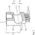
- FIG. 7 is a view of a contact element with, arranged thereon, plug-in contact elements of the subunit in FIG. 4 ;
- FIG. 8 is a sectional view of a contacting device for transmitting electrical energy from a power supply line to a circuit board, according to a second embodiment.
- FIG. 9 is a sectional view of a contacting device for transmitting electrical energy from a power supply line to a circuit board, according to a third embodiment.
- a contacting device 1 includes a preassembled subunit 2 with a housing 3 , with a first contact element 4 , with a spring element 5 and with plug-in contact elements 6 .
- the contacting device 1 further includes a second contact element 7 which is capable of being contacted with the first contact element 4 for the purpose of transmitting electrical energy to a circuit board 8 .
- the housing 3 exhibits two housing parts 9 , 10 which delimit an interior space 11 at least in some regions.
- the first housing part 9 exhibits four side walls 12 , 12 ′, 13 , 13 ′ and an upper top wall 14 , said side walls 12 , 12 ′ and also said side walls 13 , 13 ′ being situated opposite each other.
- associated openings 15 , 15 ′ have been formed which have a common first central longitudinal axis 16 and have been formed and arranged congruently in the direction of central longitudinal axis 16 .
- latching openings 18 For the purpose of forming a latching connection 17 between the housing parts 9 and 10 , in each instance two latching openings 18 have been formed in side walls 13 , 13 ′.
- a slot 19 has been formed in side walls 13 , 13 ′ between, in each instance, one of the latching openings 18 and the adjacent side wall 12 , 12 ′.
- Side walls 12 , 12 ′, 13 , 13 ′ delimit opposite the top wall 14 an assembly opening 20 for inserting the second housing part 10 .
- the second housing part 10 includes four side walls 21 , 21 ′, 22 , 22 ′, of which side walls 21 , 21 ′ and side walls 22 , 22 ′ are situated opposite each other. Openings 23 , 23 ′ substantially corresponding to openings 15 , 15 ′ have been formed in side walls 21 , 21 ′. Openings 23 , 23 ′ have a common second central longitudinal axis 24 which in the connected state of the housing parts 9 , 10 overlaps with the first central longitudinal axis 16 , so that openings 15 , 23 and 15 ′, 23 ′ are substantially congruent.
- latching projections 27 have been formed on an outside of side walls 22 , 22 ′, which in the assembled state of the housing parts 9 , 10 engage in the associated latching openings 18 .
- the assembly recess 25 has been adapted to a thickness of side walls 21 , 21 ′, 22 , 22 ′ in such a manner that the interior space 11 has a constant width in the direction of central longitudinal axes 16 , 24 and perpendicular to central longitudinal axes 16 , 24 .
- a common wall thickness of side walls 12 , 21 and 12 ′, 21 ′, respectively, and 13 , 22 and 13 ′, 22 ′, respectively, is accordingly constant.
- the second housing part 10 On a side facing away from the top wall 14 , the second housing part 10 exhibits two boundary members 28 , 28 ′.
- the boundary members 28 , 28 ′ are arranged on the respectively associated side wall 22 , 22 ′ and extend between side walls 21 , 21 ′.
- the boundary members 28 , 28 ′ terminate flush with side walls 21 , 21 ′, 22 , 22 ′.
- the boundary members 28 , 28 ′ and side walls 21 , 21 ′ delimit a passage opening 29 .
- the first contact element 4 is of cuboidal design.
- the first contact element 4 exhibits a receiving chamber 30 for the second contact element 7 , which is of cylindrical design.
- the receiving chamber 30 takes the form of a through bore and has a central longitudinal axis 31 .
- the first contact element 4 is arranged in the interior space 11 in such a manner that the central longitudinal axes 16 , 24 of the openings 15 , 15 ′, 23 , 23 ′ run parallel to central longitudinal axis 31 , and the receiving chamber 30 is open with respect to the openings 15 , 15 ′, 23 , 23 ′.
- the openings 15 , 15 ′, 23 , 23 ′ exhibit for this purpose a diameter D 1 that corresponds at least to a diameter D 2 of the receiving chamber 30 .
- the first contact element 4 is displaceable linearly in the interior space 11 perpendicular to central longitudinal axis 31 and in the direction toward the passage opening 29 .
- the first contact element 4 exhibits recesses 32 on a side facing toward the boundary members 28 , 28 ′, so that the first contact element 4 forms a guide portion 33 , guided in the housing 3 , and a passage portion 34 extending through the passage opening 29 .
- a length L 1 of the interior space 11 from the top wall 14 as far as the boundary members 28 , 28 ′, is greater than a length L 2 of the guide portion 33 , so that the first contact element 4 is displaceable perpendicular to central longitudinal axis 31 , and the top wall 14 for the guide portion 33 forms a first stop A 1 , for limiting the motion of the first contact element 4 in a first displacement direction V 1 , and the boundary members 28 , 28 ′ form a second stop A 2 for limiting the motion of the guide portion 33 in a contrary second displacement direction V 2 .
- the plug-in contact elements 6 are arranged in one piece, so that the plug-in contact elements 6 with the first contact element 4 are displaceable in the displacement directions V 1 and V 2 .
- the guide portion 33 On a side facing toward the top wall 14 , the guide portion 33 exhibits a cavity 35 in the form of a blind hole, in which the spring element 5 is arranged.
- the spring element 5 bears in biased manner against the top wall 14 and the guide portion 33 and generates a spring force perpendicular to central longitudinal axis 31 in displacement direction V 2 .
- the spring element 5 takes the form of a coil spring, for instance.
- the plug-in contact elements 6 serve for mechanical and electrical connecting of the first contact element 4 to the circuit board 8 .
- the plug-in contact elements take the form of pins, for instance.
- the plug-in contact elements 6 are capable of being plugged, in exactly fitting manner, into plug-in contact element receptacles which have been formed in the circuit board 8 , as a result of which the mechanical and the electrical connections are established.
- the second contact element 7 serves for contacting the first contact element 4 .
- the second contact element 7 comprises an insertion portion 36 , a first clamping portion 37 , a contact portion 38 , a second clamping portion 39 and a crimp portion 40 .
- the contact portion 38 is of cylindrical design and corresponds in its length and its diameter to the receiving chamber 30 , so that the contact portion 38 can be inserted in exactly fitting manner in the receiving chamber 30 .
- the clamping portions 37 , 39 are arranged on both sides of the contact portion 38 .
- the clamping portions 37 , 39 respectively include a circumferential groove 41 , 41 ′.
- the respective groove 41 , 41 ′ tapers in the direction of a groove bottom and is, for instance, of triangular design in cross-section.
- the grooves 41 , 41 ′ are spaced in the direction of central longitudinal axis 31 , corresponding to side walls 12 , 21 and 12 ′, 21 ′, and exhibit peripherally an axial dimension that is at least equal to the axial dimension of side walls 12 , 21 and 12 ′, 21 ′, so that the housing 3 is able to engage in the grooves 41 , 41 ′.
- the insertion portion 36 For the purpose of inserting into the housing 3 , the insertion portion 36 exhibits a tapering tip 42 .
- the inserting of the second contact element 7 into the housing 3 is limited by an annular stop 43 which is formed by the crimp portion 40 .
- the crimp portion 40 is of hollow cylindrical design at a free end and exhibits an insertion opening 45 .
- the housing 3 has been formed from a synthetic material.
- the contact elements 4 , 7 and the plug-in contact elements 6 have been formed from a conductive material, for instance from brass.
- the crimp portion 40 has preferentially been soft-annealed.
- the spring element 5 is arranged in the cavity 35 of the first contact element 4 . Subsequently the first contact element 4 with the spring element 5 is inserted into the first housing part 9 until the spring element 5 bears against the top wall 14 . Subsequently the second housing part 10 is connected to the first housing part 9 . For this purpose, the plug-in contact elements 6 and the passage portion 34 are guided through the passage opening 29 , so that the second housing part 10 is inserted into the assembly recess 25 of the first housing part 9 . The second housing part 10 is moved in the direction of the top wall 14 until such time as it bears against the assembly stop 26 and the latching projections 27 latch in the latching openings 18 .
- the second contact element 7 is connected to the power supply line 44 in electrically conducting manner.
- the power supply line 44 is inserted into the crimp portion 40 through the insertion opening 45 and is clamped there in electrically conducting manner by plastic deformation of the crimp portion 40 .
- the preassembled subunit 2 is connected to the circuit board 8 mechanically and in electrically conducting manner by means of the plug-in contact elements 6 , by the plug-in contact elements 6 being inserted into associated plug-in contact element receptacles. Subsequently the housing 3 is displaced in displacement direction V 1 relative to the first contact element 4 and against the spring force of the spring element 5 in such a manner that central longitudinal axis 31 is substantially congruent with central longitudinal axes 16 , 24 , and the receiving chamber 30 is in alignment with the openings 15 , 23 and 15 ′, 23 ′.
- the second contact element 7 is guided, beginning with the tip 42 , through openings 15 ′, 23 ′, through the receiving chamber 30 and through openings 15 , 23 until stop 43 strikes against side wall 13 ′.
- the second contact element 7 has been aligned relative to the first contact element 4 and the housing 3 .
- the housing 3 is displaced in displacement direction V 2 relative to the first contact element 4 by means of the spring force of the spring element 5 , as a result of which side walls 15 , 23 engage in groove 41 and side walls 15 ′, 23 ′ engage in groove 41 ′ and clamp the second contact element 7 in the receiving chamber 30 in the direction of central longitudinal axis 31 and also perpendicular to central longitudinal axis 31 .
- the spring element 5 presses the first contact element 4 against the contact portion 38 , so that an electrical contacting between the first contact element 4 and the second contact element 7 takes place.
- the contacting device 1 exhibits a small number of components and is consequently simply constructed and easy to assemble and preassemble.
- the electrical contacting has a low ohmic resistance and can be established and disengaged again in simple and reliable manner.
- the contacting device 1 exhibits precisely one plug-in contact element 6 .
- the plug-in contact element 6 takes the form of a threaded pin and exhibits an external thread 46 .
- the plug-in contact element 6 is inserted or plugged into an associated plug-in contact element receptacle of the circuit board 8 .
- the plug-in contact element receptacle exhibits a corresponding internal thread.
- the plug-in contact element 6 takes the form of a threaded bore or threaded recess.
- the plug-in contact element 6 exhibits an internal thread 47 .
- the plug-in contact element 6 is plugged or screwed onto a threaded pin 48 of the circuit board.
- the threaded pin 48 of the circuit board is connected to the circuit board 8 in conducting manner.
- the threaded pin 48 of the circuit board serves as plug-in contact element receptacle on which the plug-in contact element 6 is received.
Landscapes
- Engineering & Computer Science (AREA)
- Manufacturing & Machinery (AREA)
- Coupling Device And Connection With Printed Circuit (AREA)
Applications Claiming Priority (4)
| Application Number | Priority Date | Filing Date | Title |
|---|---|---|---|
| DE202016102669U | 2016-05-19 | ||
| DE202016102669.5U DE202016102669U1 (de) | 2016-05-19 | 2016-05-19 | Kontaktierungsvorrichtung zur elektrischen Energieübertragung zu einer Leiterplatte |
| DE202016102669.5 | 2016-05-19 | ||
| PCT/EP2017/061867 WO2017198728A1 (de) | 2016-05-19 | 2017-05-17 | Kontaktierungsvorrichtung zur elektrischen energieübertragung zu einer leiterplatte und verfahren zur montage einer derartigen kontaktierungsvorrichtung |
Publications (2)
| Publication Number | Publication Date |
|---|---|
| US20190296461A1 US20190296461A1 (en) | 2019-09-26 |
| US10601155B2 true US10601155B2 (en) | 2020-03-24 |
Family
ID=58709982
Family Applications (1)
| Application Number | Title | Priority Date | Filing Date |
|---|---|---|---|
| US16/302,353 Active US10601155B2 (en) | 2016-05-19 | 2017-05-17 | Contacting device for the transmission of electrical energy to a circuit board and method for the assembly of such a contacting device |
Country Status (9)
| Country | Link |
|---|---|
| US (1) | US10601155B2 (de) |
| EP (2) | EP3262716B1 (de) |
| CN (1) | CN109478728B (de) |
| DE (1) | DE202016102669U1 (de) |
| ES (2) | ES2686543T3 (de) |
| HK (2) | HK1246508B (de) |
| SG (1) | SG11201809389TA (de) |
| TW (1) | TWI654798B (de) |
| WO (1) | WO2017198728A1 (de) |
Cited By (1)
| Publication number | Priority date | Publication date | Assignee | Title |
|---|---|---|---|---|
| USD1125071S1 (en) | 2025-03-26 | 2026-05-05 | Molex, Llc | Connector |
Families Citing this family (5)
| Publication number | Priority date | Publication date | Assignee | Title |
|---|---|---|---|---|
| EP3027932B1 (de) | 2013-07-31 | 2018-11-21 | BeijingWest Industries Co. Ltd. | Hydraulischer aufhängungsdämpfer |
| CN112713415A (zh) * | 2020-12-14 | 2021-04-27 | 安徽鑫龙低压电器有限公司 | 一种连接器 |
| GB2622007B (en) * | 2022-08-30 | 2025-05-28 | Viper Innovations Ltd | Electrical connector |
| USD1096637S1 (en) | 2022-08-30 | 2025-10-07 | Viper Innovations Limited | Electrical connector |
| DE102023000390B3 (de) | 2023-02-08 | 2024-02-22 | Sew-Eurodrive Gmbh & Co Kg | Anschlussvorrichtung für einen elektrischen Leiter und Kontaktierungseinheit |
Citations (15)
| Publication number | Priority date | Publication date | Assignee | Title |
|---|---|---|---|---|
| GB592135A (en) | 1945-05-22 | 1947-09-09 | Crabtree & Co Ltd J A | Improvements in electric terminals |
| DE1036969B (de) | 1955-08-03 | 1958-08-21 | Hirschmann Radiotechnik | Schnellspannstecker |
| US3221291A (en) * | 1963-10-18 | 1965-11-30 | Raytheon Co | Electrical test-point connector |
| US4749357A (en) | 1985-12-23 | 1988-06-07 | Elcon Products International Company | Circuit board connector, bus and system |
| US5055055A (en) * | 1990-10-12 | 1991-10-08 | Elcon Products International Company | Circuit board connector system |
| US5807120A (en) * | 1996-03-06 | 1998-09-15 | Elcon Products International | Printed circuit board power distribution connector |
| USD435015S (en) * | 2000-05-11 | 2000-12-12 | Hon Hai Precision Ind. Co., Ltd. | Electrical connector |
| US6280245B1 (en) * | 1999-09-17 | 2001-08-28 | Tvm Group, Inc. | Dual contact power connector |
| US6319021B1 (en) * | 2000-12-19 | 2001-11-20 | Hon Hai Precision Ind. Co., Ltd. | Power connector providing improved performance |
| US6431891B1 (en) * | 2000-12-26 | 2002-08-13 | Hon Hai Precision Ind. Co., Ltd. | Power connector with easily removable conductive pin |
| US6461174B1 (en) * | 2001-09-12 | 2002-10-08 | Hon Hai Precision Ind. Co., Ltd. | Power connector more easily and cheaply manufactured |
| US7422459B2 (en) * | 2004-04-08 | 2008-09-09 | Hopper Troy K | Thermocouples and resistance temperature detectors oil-wicking seal fitting |
| US9379468B2 (en) * | 2012-10-26 | 2016-06-28 | Cisco Technology, Inc. | Apparatus and method for allowing alignment mismatch in electrical connections |
| US20180337463A1 (en) * | 2015-02-10 | 2018-11-22 | Autonetworks Technologies, Ltd. | Power distribution device |
| US10312612B2 (en) * | 2017-05-25 | 2019-06-04 | Molex, Llc | High-current connector and high-current connection device |
Family Cites Families (5)
| Publication number | Priority date | Publication date | Assignee | Title |
|---|---|---|---|---|
| GB242156A (en) * | 1925-04-01 | 1925-11-05 | Frank Valentine Breeden | Improvements in or relating to electric terminals |
| US2205244A (en) * | 1935-06-10 | 1940-06-18 | Kingston Products Corp | Electrical connection means |
| FR2696584B1 (fr) * | 1992-10-05 | 1994-12-02 | Merlin Gerin | Borne de raccordement pour appareillage électrique de puissance. |
| DE19610610A1 (de) * | 1996-03-18 | 1997-09-25 | Whitaker Corp | Anordnung zur Verbindung eines elektrischen Leiters mit einem Schneidklemmkontakt |
| FR2935202B1 (fr) * | 2008-08-21 | 2010-10-22 | Labinal | Dispositif de connexion entre un cable electrique et une structure conductrice, notamment pour circuit de retour de courant |
-
2016
- 2016-05-19 DE DE202016102669.5U patent/DE202016102669U1/de active Active
-
2017
- 2017-05-17 EP EP17724036.3A patent/EP3262716B1/de active Active
- 2017-05-17 WO PCT/EP2017/061867 patent/WO2017198728A1/de not_active Ceased
- 2017-05-17 ES ES17724036.3T patent/ES2686543T3/es active Active
- 2017-05-17 SG SG11201809389TA patent/SG11201809389TA/en unknown
- 2017-05-17 CN CN201780030406.6A patent/CN109478728B/zh active Active
- 2017-05-17 HK HK18105545.9A patent/HK1246508B/zh unknown
- 2017-05-17 ES ES18156248T patent/ES2744806T3/es active Active
- 2017-05-17 EP EP18156248.9A patent/EP3336969B1/de active Active
- 2017-05-17 US US16/302,353 patent/US10601155B2/en active Active
- 2017-05-18 TW TW106116487A patent/TWI654798B/zh active
-
2018
- 2018-07-17 HK HK18109215.0A patent/HK1249804B/zh unknown
Patent Citations (15)
| Publication number | Priority date | Publication date | Assignee | Title |
|---|---|---|---|---|
| GB592135A (en) | 1945-05-22 | 1947-09-09 | Crabtree & Co Ltd J A | Improvements in electric terminals |
| DE1036969B (de) | 1955-08-03 | 1958-08-21 | Hirschmann Radiotechnik | Schnellspannstecker |
| US3221291A (en) * | 1963-10-18 | 1965-11-30 | Raytheon Co | Electrical test-point connector |
| US4749357A (en) | 1985-12-23 | 1988-06-07 | Elcon Products International Company | Circuit board connector, bus and system |
| US5055055A (en) * | 1990-10-12 | 1991-10-08 | Elcon Products International Company | Circuit board connector system |
| US5807120A (en) * | 1996-03-06 | 1998-09-15 | Elcon Products International | Printed circuit board power distribution connector |
| US6280245B1 (en) * | 1999-09-17 | 2001-08-28 | Tvm Group, Inc. | Dual contact power connector |
| USD435015S (en) * | 2000-05-11 | 2000-12-12 | Hon Hai Precision Ind. Co., Ltd. | Electrical connector |
| US6319021B1 (en) * | 2000-12-19 | 2001-11-20 | Hon Hai Precision Ind. Co., Ltd. | Power connector providing improved performance |
| US6431891B1 (en) * | 2000-12-26 | 2002-08-13 | Hon Hai Precision Ind. Co., Ltd. | Power connector with easily removable conductive pin |
| US6461174B1 (en) * | 2001-09-12 | 2002-10-08 | Hon Hai Precision Ind. Co., Ltd. | Power connector more easily and cheaply manufactured |
| US7422459B2 (en) * | 2004-04-08 | 2008-09-09 | Hopper Troy K | Thermocouples and resistance temperature detectors oil-wicking seal fitting |
| US9379468B2 (en) * | 2012-10-26 | 2016-06-28 | Cisco Technology, Inc. | Apparatus and method for allowing alignment mismatch in electrical connections |
| US20180337463A1 (en) * | 2015-02-10 | 2018-11-22 | Autonetworks Technologies, Ltd. | Power distribution device |
| US10312612B2 (en) * | 2017-05-25 | 2019-06-04 | Molex, Llc | High-current connector and high-current connection device |
Cited By (1)
| Publication number | Priority date | Publication date | Assignee | Title |
|---|---|---|---|---|
| USD1125071S1 (en) | 2025-03-26 | 2026-05-05 | Molex, Llc | Connector |
Also Published As
| Publication number | Publication date |
|---|---|
| DE202016102669U1 (de) | 2017-08-22 |
| HK1249804B (zh) | 2020-03-20 |
| EP3262716B1 (de) | 2018-06-27 |
| EP3336969A1 (de) | 2018-06-20 |
| TWI654798B (zh) | 2019-03-21 |
| US20190296461A1 (en) | 2019-09-26 |
| SG11201809389TA (en) | 2018-12-28 |
| WO2017198728A1 (de) | 2017-11-23 |
| CN109478728B (zh) | 2021-02-26 |
| ES2686543T3 (es) | 2018-10-18 |
| EP3262716A1 (de) | 2018-01-03 |
| HK1246508B (zh) | 2019-07-05 |
| TW201803217A (zh) | 2018-01-16 |
| CN109478728A (zh) | 2019-03-15 |
| ES2744806T3 (es) | 2020-02-26 |
| EP3336969B1 (de) | 2019-06-26 |
Similar Documents
| Publication | Publication Date | Title |
|---|---|---|
| US10601155B2 (en) | Contacting device for the transmission of electrical energy to a circuit board and method for the assembly of such a contacting device | |
| US9806451B2 (en) | Connector and contacts assembly | |
| CN104919657B (zh) | 用于半导体模块的电压配销 | |
| US9318831B2 (en) | Connector | |
| US20160064862A1 (en) | Control Assembly | |
| JP2016050882A (ja) | 温度センサ | |
| HK1246508A1 (en) | Contacting device for the transmission of electrical energy to a circuit board and method for the assembly of such a contacting device | |
| HK1249804A1 (en) | Contacting device for transfer of electric energy to a printed circuit board and a method for assembling such a contacting device | |
| CN107078264B (zh) | 蓄能器设备,接触元件和用于制造蓄能器设备的方法 | |
| KR20090006701U (ko) | 수직형 터미널조립체 | |
| KR20150096306A (ko) | 전자 장치 | |
| JP2016024928A (ja) | コネクタ装置 | |
| US9755349B1 (en) | Connector assembly with blocking member | |
| US3113553A (en) | Connector with indicator | |
| CN105745791A (zh) | 具有护套夹的电连接器 | |
| US20230335945A1 (en) | Connector | |
| CN205693009U (zh) | 长寿命的导电弹片及具有其的智能排插 | |
| CN110571367A (zh) | 电池装置及电池固定架 | |
| CN216098526U (zh) | 一种同轴器安装治具 | |
| CN217791465U (zh) | 连接方便的电子雾化器 | |
| KR102634968B1 (ko) | 차량용 터미널 | |
| CN222980835U (zh) | 一种电连接器 | |
| CN218551269U (zh) | 弹簧结构的雾化器 | |
| CN223911971U (zh) | 一种可准确组装的智能开关 | |
| CN110896180B (zh) | 联接耦合装置、存储系统以及带有联接耦合装置的机动车 |
Legal Events
| Date | Code | Title | Description |
|---|---|---|---|
| FEPP | Fee payment procedure |
Free format text: ENTITY STATUS SET TO UNDISCOUNTED (ORIGINAL EVENT CODE: BIG.); ENTITY STATUS OF PATENT OWNER: LARGE ENTITY |
|
| AS | Assignment |
Owner name: WUERTH ELEKTRONIK EISOS GMBH & CO. KG, GERMANY Free format text: ASSIGNMENT OF ASSIGNORS INTEREST;ASSIGNOR:WERZ, WLADIMIR;REEL/FRAME:050890/0033 Effective date: 20181121 |
|
| STPP | Information on status: patent application and granting procedure in general |
Free format text: NOTICE OF ALLOWANCE MAILED -- APPLICATION RECEIVED IN OFFICE OF PUBLICATIONS |
|
| STPP | Information on status: patent application and granting procedure in general |
Free format text: PUBLICATIONS -- ISSUE FEE PAYMENT VERIFIED |
|
| STCF | Information on status: patent grant |
Free format text: PATENTED CASE |
|
| MAFP | Maintenance fee payment |
Free format text: PAYMENT OF MAINTENANCE FEE, 4TH YEAR, LARGE ENTITY (ORIGINAL EVENT CODE: M1551); ENTITY STATUS OF PATENT OWNER: LARGE ENTITY Year of fee payment: 4 |