US10680594B2 - Comparator circuit with feedback and method of operation - Google Patents
Comparator circuit with feedback and method of operation Download PDFInfo
- Publication number
- US10680594B2 US10680594B2 US16/030,945 US201816030945A US10680594B2 US 10680594 B2 US10680594 B2 US 10680594B2 US 201816030945 A US201816030945 A US 201816030945A US 10680594 B2 US10680594 B2 US 10680594B2
- Authority
- US
- United States
- Prior art keywords
- coupled
- voltage
- circuit
- transistor
- input
- Prior art date
- Legal status (The legal status is an assumption and is not a legal conclusion. Google has not performed a legal analysis and makes no representation as to the accuracy of the status listed.)
- Active, expires
Links
Images



Classifications
-
- H—ELECTRICITY
- H03—ELECTRONIC CIRCUITRY
- H03K—PULSE TECHNIQUE
- H03K5/00—Manipulating of pulses not covered by one of the other main groups of this subclass
- H03K5/22—Circuits having more than one input and one output for comparing pulses or pulse trains with each other according to input signal characteristics, e.g. slope, integral
- H03K5/24—Circuits having more than one input and one output for comparing pulses or pulse trains with each other according to input signal characteristics, e.g. slope, integral the characteristic being amplitude
-
- G—PHYSICS
- G01—MEASURING; TESTING
- G01R—MEASURING ELECTRIC VARIABLES; MEASURING MAGNETIC VARIABLES
- G01R19/00—Arrangements for measuring currents or voltages or for indicating presence or sign thereof
- G01R19/165—Indicating that current or voltage is either above or below a predetermined value or within or outside a predetermined range of values
- G01R19/16533—Indicating that current or voltage is either above or below a predetermined value or within or outside a predetermined range of values characterised by the application
- G01R19/16538—Indicating that current or voltage is either above or below a predetermined value or within or outside a predetermined range of values characterised by the application in AC or DC supplies
- G01R19/16547—Indicating that current or voltage is either above or below a predetermined value or within or outside a predetermined range of values characterised by the application in AC or DC supplies voltage or current in AC supplies
-
- G—PHYSICS
- G01—MEASURING; TESTING
- G01R—MEASURING ELECTRIC VARIABLES; MEASURING MAGNETIC VARIABLES
- G01R31/00—Arrangements for testing electric properties; Arrangements for locating electric faults; Arrangements for electrical testing characterised by what is being tested not provided for elsewhere
- G01R31/40—Testing power supplies
-
- G—PHYSICS
- G06—COMPUTING OR CALCULATING; COUNTING
- G06F—ELECTRIC DIGITAL DATA PROCESSING
- G06F1/00—Details not covered by groups G06F3/00 - G06F13/00 and G06F21/00
- G06F1/26—Power supply means, e.g. regulation thereof
- G06F1/28—Supervision thereof, e.g. detecting power-supply failure by out of limits supervision
-
- H—ELECTRICITY
- H03—ELECTRONIC CIRCUITRY
- H03K—PULSE TECHNIQUE
- H03K3/00—Circuits for generating electric pulses; Monostable, bistable or multistable circuits
- H03K3/02—Generators characterised by the type of circuit or by the means used for producing pulses
- H03K3/027—Generators characterised by the type of circuit or by the means used for producing pulses by the use of logic circuits, with internal or external positive feedback
- H03K3/037—Bistable circuits
-
- H—ELECTRICITY
- H03—ELECTRONIC CIRCUITRY
- H03K—PULSE TECHNIQUE
- H03K5/00—Manipulating of pulses not covered by one of the other main groups of this subclass
- H03K5/22—Circuits having more than one input and one output for comparing pulses or pulse trains with each other according to input signal characteristics, e.g. slope, integral
- H03K5/24—Circuits having more than one input and one output for comparing pulses or pulse trains with each other according to input signal characteristics, e.g. slope, integral the characteristic being amplitude
- H03K5/2472—Circuits having more than one input and one output for comparing pulses or pulse trains with each other according to input signal characteristics, e.g. slope, integral the characteristic being amplitude using field effect transistors
-
- G—PHYSICS
- G01—MEASURING; TESTING
- G01R—MEASURING ELECTRIC VARIABLES; MEASURING MAGNETIC VARIABLES
- G01R19/00—Arrangements for measuring currents or voltages or for indicating presence or sign thereof
- G01R19/165—Indicating that current or voltage is either above or below a predetermined value or within or outside a predetermined range of values
- G01R19/16566—Circuits and arrangements for comparing voltage or current with one or several thresholds and for indicating the result not covered by subgroups G01R19/16504, G01R19/16528, G01R19/16533
- G01R19/16576—Circuits and arrangements for comparing voltage or current with one or several thresholds and for indicating the result not covered by subgroups G01R19/16504, G01R19/16528, G01R19/16533 comparing DC or AC voltage with one threshold
-
- H—ELECTRICITY
- H03—ELECTRONIC CIRCUITRY
- H03K—PULSE TECHNIQUE
- H03K19/00—Logic circuits, i.e. having at least two inputs acting on one output; Inverting circuits
- H03K19/20—Logic circuits, i.e. having at least two inputs acting on one output; Inverting circuits characterised by logic function, e.g. AND, OR, NOR, NOT circuits
Definitions
- This disclosure relates generally to integrated circuits, and more specifically, to a comparator circuit with feedback.
- SoCs System on Chips
- SoCs System on Chips
- the supply voltage is altered in order to make a device or System on Chip (SoC) more vulnerable.
- fault injection attacks are commonly performed by tampering with the supply voltage in order to maliciously alter software execution. Therefore, it is useful, for safety and security purposes, to have a comparator able to detect such variations in the supply voltage.
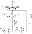
- FIG. 1 illustrates, in schematic form, a comparator circuit in accordance with one embodiment of the present invention.
- FIG. 2 illustrates, in block diagram form, an SoC containing the comparator circuit of FIG. 1 , in accordance with one embodiment of the present invention.
- FIG. 3 illustrates, in partial block diagram and partial schematic form, an SoC containing the comparator circuit of FIG. 1 and a pad segment containing multiple pads, in accordance with one embodiment of the present invention.
- FIG. 4 illustrates, in flow diagram form, a method of operation the SoC of FIG. 3 , in accordance with one example of the present invention.
- a low power coarse comparator compares two direct-current (DC) voltage levels.
- This comparator may be used, for example, to detect an over voltage situation.
- This comparator consumes negligible DC current due to a feedback mechanism that automatically disables the comparator when the output switches. In this manner, the comparator consumes low power and can remain on.
- the comparator circuit can be used to detect a supply voltage tampering or incompatibility event and assert a fault indicator in response thereto.
- such a comparator circuit along with a digital controller, can be used to detect supply voltage incompatibility for an entire pad segment.
- FIG. 1 illustrates, in schematic form, a comparator circuit 10 in accordance with one embodiment of the present invention.
- Comparator circuit 10 includes P-channel transistors 12 , 14 , 24 , and 28 and N-channel transistors 18 , 20 , 22 , 26 , and 30 .
- a control electrode of transistor 12 is coupled to receive a first DC input voltage, V 1
- a first current electrode of transistor 12 is coupled to receive a second DC input voltage, V 2 .
- the first DC input V 1 corresponds to an inverting input of comparator circuit 10
- the second DC input V 2 corresponds to a non-inverting input of comparator circuit 10 .
- Transistor 14 has a first current electrode coupled to a second current electrode of transistor 12 , a control electrode coupled to receive enb, and a second current electrode coupled to circuit node 16 .
- an active high enable signal, en can be used to enable comparator circuit 10
- enb is the inverse of en (and thus an active low enable signal for comparator circuit 10 ).
- Body terminals of transistors 12 and 14 are coupled to V 2 .
- Transistor 18 has a first current electrode coupled to node 16 , a control electrode coupled to node 16 , and a second current electrode.
- Transistor 20 has a first current electrode coupled to the second current electrode of transistor 18 , a control electrode coupled to receive a feedback signal from a circuit node 36 , and a second current electrode coupled to a first voltage supply terminal, dvss.
- the body terminals of transistors 18 and 20 are coupled to dvss.
- Transistor 22 has a first current electrode coupled to node 16 , a control electrode coupled to receive enb, a second current electrode coupled to dvss, and a body terminal coupled to dvss.
- transistor 24 has a first current electrode and body terminal coupled to a second voltage supply terminal, vdde, a control electrode coupled to node 16 , and a second current electrode coupled to node 36 .
- Transistor 26 has a first current electrode coupled to node 36 , a control electrode coupled to node 16 , and a second current electrode and body terminal coupled to dvss.
- Transistor 28 has a first current electrode and body terminal coupled to a third voltage supply terminal, dvdd, a control electrode coupled to node 36 , and a second current electrode coupled to an output node, out 38 , of comparator circuit 10 .
- Transistor 30 has a first current electrode coupled to out 38 , a control electrode coupled to node 36 , and a second current electrode and body terminal coupled to dvss.
- vdde is greater than dvdd which are greater than dvss.
- Transistors 24 and 26 operate as an inverter 32
- transistors 28 and 30 operate as an inverter 34 .
- Inverter 32 inverts the polarity of node 16 and provides the inverted value to inverter 34 .
- Inverter 34 inverts the polarity of node 36 and provides out 38 with the correct polarity (matching the polarity of node 16 ) but level shifted from vdde to dvdd.
- Node 36 corresponds to an output of inverter 32 , which provides the feedback signal to the control electrode of transistor 18 .
- V 2 is less than (V 1 +threshold voltage of transistor 12 , Vtp)
- the output is low, i.e. dvss
- V 1 +Vtp the output switches to high, i.e. dvdd.
- the first input, V 1 is fixed by being coupled to vdde
- the second input, V 2 is monitored to determine when it surpasses V 1 by Vtp.
- en is 0 (meaning enb is 1). This maintains transistor 14 off and transistor 22 on.
- Transistor 22 pulls node 16 down to dvss, causing node 36 to go high. With node 36 high, the feedback to transistor 20 turns on transistor 20 . With transistor 20 on, node 16 is pulled down, via transistor 18 , to ground.
- comparator circuit 10 is enabled by changing en to 1 and, thus, enb to 0. This turns off transistor 22 and turns on transistor 14 . At this point, comparator circuit 10 is in its monitoring state. So long as V 2 is less than or equal to V 1 +Vtp, transistor 12 is off. The feedback from node 36 to transistor 20 is still held high so transistor 20 is maintained on and pulls down node 16 . While comparator circuit 10 is in its monitoring state, there is no DC current in the comparator.
- transistor 12 When V 2 goes above V 1 by Vtp, transistor 12 turns on and, with enb being 0, transistor 14 is still on. Transistor 14 begins to slowly ramp up node 16 . Since transistors 18 and 20 are still on and pulling down on node 16 , there is contention on node 16 . However, as node 16 increases, due to the feedback provided by node 36 , transistor 20 starts turning off. In the illustrated embodiment, transistor 18 is coupled as a resistive element and operates as a weak load. Therefore, node 16 is eventually pulled up by transistors 12 and 14 to V 2 . This causes the feedback at node 36 to go low, turning off transistor 20 , and causes out 38 to go high, indicating a fault corresponding to an over voltage condition. With transistor 20 off, there is no DC current path anymore.
- comparator circuit 10 With node 16 now pulled up to V 2 , comparator circuit 10 has to be reset by way of negating and subsequently asserting en. Therefore, once out 38 changes state from low to high, en has to be toggled to reset comparator 10 again into its monitoring state. In this manner, out 38 will only be triggered (asserted) once since the enabling of comparator circuit 10 to indicate a fault.
- Transistor 18 is coupled as a resistive element and represents the load of comparator circuit 10 .
- any resistive element or active load can be used which provides a weak load that can be pulled by the p-channel transistors 12 and 14 .
- a predetermined margin of Vtp is used in the comparison of V 1 and V 2 .
- Vtp could be generated using a resistor divider and used instead of V 2 in the comparator. In this case, there would be no Vtp margin in the comparison.
- FIG. 2 illustrates, in block diagram form, a printed circuit board (PCB) 50 containing an SoC 62 and a supply domain 58 powering SoC 62 .
- SoC 62 includes an input/output (I/O) domain 54 which has a supply pad 60 .
- Supply domain 58 is coupled to provide power to pad 60 .
- SoC 62 also includes comparator circuit 10 (as was described with respect to FIG. 1 ), a controller 52 , and fault logging circuitry 56 .
- Fault logging circuitry 56 provides a fault notification to users.
- I/O domain 54 is powered by VDDIO. That is, the circuitry in I/O domain 54 receives VDDIO as a power supply voltage.
- the inverting input of comparator circuit 10 (corresponding to V 1 of FIG.
- Controller 52 provides enb to comparator circuit 10 , and receives out 38 from comparator circuit 10 . Controller 52 is coupled to provide fault indications to fault logging circuitry 56 in response to assertions of out 38 , and fault logging circuitry 56 outputs these fault indications external to SoC 62 .
- supply domain 58 is a first power supply domain and I/O domain 54 is a second power supply domain.
- supply domain 58 is coupled to pad 60 to supply a compatible supply voltage to I/O domain 54 for proper circuit operation. If supply domain 58 supplies a supply voltage that is too high, damage may occur to circuitry in I/O domain 54 , or, I/O domain 54 may become vulnerable to attacks. Therefore, comparator circuit 10 monitors the voltage on pad 60 with respect to VDDIO. Controller 52 , upon powering up, enables comparator circuit 10 by asserting en to 1 and enb to 0, as described above in reference to FIG. 1 . Comparator circuit 10 is then in its monitoring state, and out 38 is low (dvss).
- controller 52 receives this indication of a fault or over-voltage condition, and provides such indication to fault logging 56 . Controller 52 may provide additional information such as time stamping information to be stored along with the fault indication by fault logging circuitry 56 . Upon receiving an assertion of out 38 , controller 52 can then toggle en so as to reset comparator circuit 10 .
- controller 52 may deassert en to 0, wait a predetermined amount of time, and then again assert en to 1.
- enb is provided to comparator circuit 10 , however, in alternate embodiments, en may be provided instead in which comparator circuit 10 would include an additional inverter to receive en and provide enb.
- FIG. 3 illustrates, in partial schematic and partial block diagram form, an SoC 100 in which comparator circuit 10 is used to provide fault (or over-voltage) detection for multiple pads in a pad segment.
- SoC 100 includes N I/O domains, I/O domain 1 to I/O domain N, and each I/O domain has a corresponding I/O pad, pad 1 to pad N, respectively, and is powered by VDDIO.
- Pad 1 to pad N and I/O domain 1 to I/O domain N correspond to a pad segment 108 .
- SoC 100 also includes a toggle flip flop 104 , inverter 106 , fault logging circuitry 116 , digital controller 102 , and switches 110 .
- VDDIO is coupled to the inverting input of comparator circuit 10 (corresponding to V 1 of FIG. 1 ), and each pad is coupled to the non-inverting input of comparator circuit 10 (corresponding to V 2 of FIG. 1 ) via a corresponding switch from set of switches 110 . Therefore, only one selected pad of pad 1 to pad N is coupled to the non-inverting input of comparator circuit 10 at a time.
- Digital controller 102 provides a pad select signal to switches 110 which selects a switch from set of switches 110 to couple a selected pad to the non-inverting input. Note that only one comparator circuit 10 is needed for pad segment 108 , in which comparator circuit 10 is shared among all pads in pad segment 108 .
- Toggle flip flop 104 is a D flip flop configured as a toggle flip flop in which a data output Q of flip flop 104 is coupled to an input of inverter 106 , and an output of inverter 106 is coupled to a data input D of flip flop 104 .
- Flip flop 104 also includes a clock input, CLK, and a reset input, RST.
- RST Upon asserting RST, such as by providing a logic level 1 to RST, the data output Q is reset to 0.
- the value at D which is 1 initially after reset, is clocked into flip flop 104 such that the data output Q is toggled from 0 to 1.
- the value at D which is now 0, is clocked into flip flop 104 such that the data output Q is now toggled from 1 to 0.
- the output of comparator circuit 10 , out 38 is coupled to CLK of flip flop 104 , and digital controller 102 receives Q and provides a reset input to RST. In this manner, the value of Q is toggled when out 38 is asserted from 0 to 1. Therefore, in one embodiment, data controller 102 first asserts the RST input to cause Q to reset to 0. Upon out 38 going high, indicating a fault, the data output Q of flip flop 104 toggles from 0 to 1. This change in Q is detected by digital controller 102 .
- Digital controller 102 upon detecting a change in Q from 0 to 1, provides information to fault logging circuitry 116 which is configured to log (i.e. store) an indication of the fault occurrence, and may store other information related to the fault, such as, for example, a time stamp and pad number.
- the time stamp and pad number can also be provided by digital controller 102 to fault logging circuitry 116 .
- RST and CLK inputs can be reversed in polarity such that providing a 0 to the RST input resets the flop or a falling edge at CLK changes the state of the data output Q.
- other edge transition capturing circuitry may be used to implement the signal edge capture and storage other than a toggle flip flop.
- the detection circuit is enabled.
- the detection circuit refers to comparator circuit 10 which operates to detect a fault condition in which a pad voltage is incompatible with VDDIO, i.e. that the pad voltage deviates from VDDIO by more than a predetermined margin.
- Enabling the detection circuit is performed by digital controller 102 which first deasserts the enable signal, en, and then asserts the enable signal, en, in which enb is asserted to a 0. This causes out 38 to reset to 0.
- Digital controller 102 resets flip flop 104 in block 154 , in which the RST input of flip flop 104 is asserted. This causes the data output Q to reset to 0.
- a pad(i) is selected from pad 1 to pad N, and this pad is coupled to the non-inverting input of comparator circuit 10 via its corresponding switch from set of switches 110 .
- digital controller 102 provides the appropriate pad select signal to switches 110 which closes the switch corresponding to pad(i) by placing that switch into a conductive state.
- pad(i) is coupled to comparator circuit 10 in which the voltage on pad(i) is being monitored (i.e. compared) against VDDIO for a predetermined amount of time (at block 158 ). If, during this time, the voltage on pad(i) goes above VDDIO+Vtp, out 38 changes from 0 to 1, causing Q to toggle from 0 to 1. If, however, the voltage on pad(i) remains at or below VDDIO during this time, out 38 does not change state and remains at 0 . Then, in block 160 , the output of the detection circuit, provided by Q, is logged into an internal register of digital controller 102 .
- fault logging circuitry 116 At decision diamond 162 , if all pads have been coupled, in turn, to the non-inverting input of comparator circuit 10 , the fault status is sent to fault logging circuitry 116 at block 164 . However, if all pads have not been completed, method 150 returns to block 152 , in which en is again deasserted and then asserted to reset out 38 to 0, and flip flop 104 is reset to reset Q to 0. A next pad is selected in block 156 to couple to the non-inverting input of comparator circuit 10 . This continues until all pads have been completed. Therefore, upon completion of monitoring all pads of pad segment 108 , fault logging circuitry 116 can provide notification of the occurrence of faults within SoC 100 .
- V 2 can be set to a secure or fixed supply and V 1 can be the voltage being monitored.
- V 1 when V 1 is greater than V 2 , operating conditions are safe, but when V 1 drops below a certain voltage, set by V 2 and any predetermined margin corresponding to Vtp drops, out 38 of comparator circuit 10 switches, indicating a fault or unsafe condition.
- V 1 drops below V 2 , it is possible for hackers to introduce a clock glitch which can result in a lack of stability and allow, for example, for code execution to be altered or otherwise affected.
- a comparator circuit utilizing feedback can monitor and detect two voltage sources, which may also be close to or above the comparator supply, to determine when an over-voltage or fault condition occurs.
- the comparator circuit may detect a deviation of one voltage source from another by a predetermined margin.
- the use of the feedback ensures that while the comparator circuit is monitoring for the deviation of one voltage source from another, no DC current is consumed.
- assert or “set” and “negate” (or “deassert” or “clear”) are used herein when referring to the rendering of a signal, status bit, or similar apparatus into its logically true or logically false state, respectively. If the logically true state is a logic level one, the logically false state is a logic level zero. And if the logically true state is a logic level zero, the logically false state is a logic level one.
- Each signal described herein may be designed as positive or negative logic, where negative logic can be indicated by a bar over the signal name or an asterix (*) following the name.
- negative logic the signal is active low where the logically true state corresponds to a logic level zero.
- positive logic the signal is active high where the logically true state corresponds to a logic level one.
- any of the signals described herein can be designed as either negative or positive logic signals. Therefore, in alternate embodiments, those signals described as positive logic signals may be implemented as negative logic signals, and those signals described as negative logic signals may be implemented as positive logic signals.
- Coupled is not intended to be limited to a direct coupling or a mechanical coupling.
- a comparator circuit includes a first transistor have a control electrode coupled to a first input voltage, a first current electrode coupled to a second input voltage, and a second current electrode coupled to a first circuit node; a first inverter coupled to a first voltage supply terminal and having a first input coupled to the first circuit node and an output; a second transistor having a control electrode coupled to the output of the first inverter; and an active resistive element coupled in series between the first circuit node and a first current electrode of the second transistor.
- the second transistor has a second current electrode coupled to a second voltage supply terminal configured to provide a lower voltage than the first voltage supply terminal.
- the circuit further includes a second inverter having a first input coupled to the output of the first inverter and having an output configured to provide an output of the comparator circuit.
- the output of the comparator circuit is negated to indicate no fault condition while the second input voltage is less than or equal to the first input voltage.
- the output of the comparator circuit is asserted to indicate a fault condition when the second input voltage is greater than the first input voltage by a predetermined margin.
- the predetermined margin corresponds to at least a threshold voltage of the first transistor.
- the second inverter is coupled to a third voltage supply terminal which is less than the second voltage supply terminal, wherein the first and second inverters are configured to level shift a voltage at the first circuit node to provide the output of the comparator circuit.
- the circuit further includes a third transistor coupled between the first transistor and the first circuit node, wherein the third transistor has a first current electrode coupled to the second current electrode of the first transistor, a second current electrode coupled to the first circuit node, and a control electrode coupled to receive an enable signal.
- the circuit further includes a fourth transistor having a first current electrode coupled to the first circuit node, a second current electrode coupled to the second voltage supply terminal, and a control electrode coupled to receive the enable signal.
- the first and third transistors are p-channel transistors and the second and fourth transistors are n-channel transistors.
- a system-on-chip includes a detector circuit having a first input coupled to a first voltage supply terminal of the SoC, a second input coupled to an input/output (I/O) pad of the SoC, and an output to provide a fault indicator
- the detector circuit includes: a first transistor have a control electrode coupled to the first input, a first current electrode coupled to the second input, and a second current electrode coupled to a first circuit node, a first inverter coupled to a first voltage supply terminal and having a first input coupled to the first circuit node and an output, a second inverter coupled in series with the first inverter and having an output configured to provide the fault indicator, a second transistor having a control electrode coupled to the output of the first inverter, and an active resistive element coupled in series between the first circuit node and a first current electrode of the second transistor; and a controller configured to enable the detector circuit and coupled to receive the fault indicator from the detector circuit.
- the SoC further includes first voltage domain circuitry coupled to the I/O pad and the first voltage supply terminal.
- the detector circuit further includes: a third transistor coupled between the first transistor and the first circuit node, wherein the third transistor has a first current electrode coupled to the second current electrode of the first transistor, a second current electrode coupled to the first circuit node, and a control electrode coupled to receive an enable signal from the controller; and a fourth transistor having a first current electrode coupled to the first circuit node, a second current electrode coupled to the second voltage supply terminal, and a control electrode coupled to receive the enable signal from the controller.
- the fault indicator is negated to indicate no fault condition while a voltage at the I/O pad is less than or equal to a voltage on the first voltage supply terminal, and the fault indicator is asserted to indicate a fault condition when the voltage at the I/O pad is greater than the voltage at the first voltage supply terminal by a predetermined margin.
- the controller in response to assertion of the fault indicator, is configured to disable and subsequently enable the detector circuit to reset the fault indicator.
- the SoC further includes fault logging circuitry coupled to the controller and configured to store indications of asserted fault indicators received by the controller and provide notification of the indications external to the SoC.
- a method of fault detection in a System on Chip (SoC) having a plurality of input/output (I/O) pads, each coupled to a first voltage supply terminal, and a detector circuit configured to provide a fault indicator includes: coupling a selected one of the plurality of I/O pads to a non-inverting input of the detector circuit, wherein the detector circuit includes: an inverting input coupled to the first voltage supply terminal, a first transistor have a control electrode coupled to the first voltage supply terminal, a first current electrode coupled to the selected one of the plurality of I/O pads, and a second current electrode coupled to a first circuit node, a first inverter coupled to a first voltage supply terminal and having a first input coupled to the first circuit node and an output, a second inverter coupled in series with the first inverter and having an output configured to provide a fault indicator, a second transistor having a control electrode coupled to the output of the first inverter, an active resistive element coupled in series between the first circuit no
- the SoC further includes a flip flop having a clock input coupled to the output of the second inverter to receive the fault indicator, a data input coupled to an inverse of a data output, and a reset input, wherein, prior to coupling the selected one of the plurality of I/O pads to the non-inverting input of the detector circuit, the method further includes enabling the detector circuit to reset the fault indicator to a negated value; and resetting the flip flop such that the data output of the data flip flop is reset to a predetermined value.
- the method further includes, after the using the detector circuit to compare a voltage at the selected one of the plurality of I/O pads to a voltage at the first voltage supply terminal over a predetermined period of time, the method further includes disabling and re-enabling the detector circuit after the predetermined period of time to reset the fault indicator to the negated value.
- the method further includes resetting the flip flop; coupling a second selected one of the plurality of I/O pads to the non-inverting input of the detector circuit; and using the detector circuit to compare a voltage at the second selected one of the plurality of I/O pads to a voltage at the first voltage supply terminal over a predetermined period of time, wherein the fault indicator is asserted by the detector circuit during the predetermined period of time when the voltage at the second selected one of the plurality of I/O pads exceeds the voltage at the first voltage supply terminal by a predetermined margin.
Landscapes
- Physics & Mathematics (AREA)
- General Physics & Mathematics (AREA)
- Engineering & Computer Science (AREA)
- Nonlinear Science (AREA)
- Theoretical Computer Science (AREA)
- Power Engineering (AREA)
- General Engineering & Computer Science (AREA)
- Logic Circuits (AREA)
- Semiconductor Integrated Circuits (AREA)
- Electronic Switches (AREA)
Priority Applications (2)
| Application Number | Priority Date | Filing Date | Title |
|---|---|---|---|
| US16/030,945 US10680594B2 (en) | 2018-07-10 | 2018-07-10 | Comparator circuit with feedback and method of operation |
| EP19183691.5A EP3595174A3 (de) | 2018-07-10 | 2019-07-01 | Komparatorschaltung mit rückkopplung und verfahren zum betrieb |
Applications Claiming Priority (1)
| Application Number | Priority Date | Filing Date | Title |
|---|---|---|---|
| US16/030,945 US10680594B2 (en) | 2018-07-10 | 2018-07-10 | Comparator circuit with feedback and method of operation |
Publications (2)
| Publication Number | Publication Date |
|---|---|
| US20200021279A1 US20200021279A1 (en) | 2020-01-16 |
| US10680594B2 true US10680594B2 (en) | 2020-06-09 |
Family
ID=67137862
Family Applications (1)
| Application Number | Title | Priority Date | Filing Date |
|---|---|---|---|
| US16/030,945 Active 2038-09-08 US10680594B2 (en) | 2018-07-10 | 2018-07-10 | Comparator circuit with feedback and method of operation |
Country Status (2)
| Country | Link |
|---|---|
| US (1) | US10680594B2 (de) |
| EP (1) | EP3595174A3 (de) |
Cited By (1)
| Publication number | Priority date | Publication date | Assignee | Title |
|---|---|---|---|---|
| US11296716B1 (en) * | 2020-12-04 | 2022-04-05 | Nxp Usa, Inc. | Analog multiplexer with current injection protection |
Families Citing this family (2)
| Publication number | Priority date | Publication date | Assignee | Title |
|---|---|---|---|---|
| CN115720657A (zh) * | 2020-06-02 | 2023-02-28 | 微芯片技术股份有限公司 | 在芯片处的故障注入事件检测以及相关系统、方法和设备 |
| US11977664B2 (en) | 2021-11-19 | 2024-05-07 | Nxp Usa, Inc. | Supply voltage proportionality monitoring in a system-on-chip (SOC) |
Citations (11)
| Publication number | Priority date | Publication date | Assignee | Title |
|---|---|---|---|---|
| US4410813A (en) * | 1981-08-14 | 1983-10-18 | Motorola, Inc. | High speed CMOS comparator circuit |
| US4590391A (en) | 1983-12-19 | 1986-05-20 | Unitrode Corporation | Multi-input zero offset comparator |
| US6147517A (en) | 1997-10-01 | 2000-11-14 | Sipex Corporation | Voltage comparator circuit |
| US20050218943A1 (en) | 2004-04-06 | 2005-10-06 | Padhye Milind P | State retention within a data processing system |
| US7003421B1 (en) | 2003-11-03 | 2006-02-21 | Lsi Logic Corporation | VDD over and undervoltage measurement techniques using monitor cells |
| US7030682B2 (en) | 2002-09-11 | 2006-04-18 | Mitsubishi Denki Kabushiki Kaisha | Voltage detection circuit and internal voltage generating circuit comprising it |
| US7639049B2 (en) | 2004-02-23 | 2009-12-29 | Rohm Co. Ltd. | Voltage detecting circuit and battery device using same |
| US20150117120A1 (en) | 2013-10-31 | 2015-04-30 | International Business Machines Corporation | Gated-feedback sense amplifier for single-ended local bit-line memories |
| US20160098333A1 (en) | 2014-10-07 | 2016-04-07 | Nuvoton Technology Corporation | Detection of fault injection attacks |
| US20160276988A1 (en) | 2015-03-16 | 2016-09-22 | Samsung Electro-Mechanics Co., Ltd. | Voltage detecting circuit and power amplifier |
| US9543752B2 (en) | 2013-09-24 | 2017-01-10 | Broadcom Corporation | Overvoltage protection circuit with digital control |
-
2018
- 2018-07-10 US US16/030,945 patent/US10680594B2/en active Active
-
2019
- 2019-07-01 EP EP19183691.5A patent/EP3595174A3/de not_active Withdrawn
Patent Citations (11)
| Publication number | Priority date | Publication date | Assignee | Title |
|---|---|---|---|---|
| US4410813A (en) * | 1981-08-14 | 1983-10-18 | Motorola, Inc. | High speed CMOS comparator circuit |
| US4590391A (en) | 1983-12-19 | 1986-05-20 | Unitrode Corporation | Multi-input zero offset comparator |
| US6147517A (en) | 1997-10-01 | 2000-11-14 | Sipex Corporation | Voltage comparator circuit |
| US7030682B2 (en) | 2002-09-11 | 2006-04-18 | Mitsubishi Denki Kabushiki Kaisha | Voltage detection circuit and internal voltage generating circuit comprising it |
| US7003421B1 (en) | 2003-11-03 | 2006-02-21 | Lsi Logic Corporation | VDD over and undervoltage measurement techniques using monitor cells |
| US7639049B2 (en) | 2004-02-23 | 2009-12-29 | Rohm Co. Ltd. | Voltage detecting circuit and battery device using same |
| US20050218943A1 (en) | 2004-04-06 | 2005-10-06 | Padhye Milind P | State retention within a data processing system |
| US9543752B2 (en) | 2013-09-24 | 2017-01-10 | Broadcom Corporation | Overvoltage protection circuit with digital control |
| US20150117120A1 (en) | 2013-10-31 | 2015-04-30 | International Business Machines Corporation | Gated-feedback sense amplifier for single-ended local bit-line memories |
| US20160098333A1 (en) | 2014-10-07 | 2016-04-07 | Nuvoton Technology Corporation | Detection of fault injection attacks |
| US20160276988A1 (en) | 2015-03-16 | 2016-09-22 | Samsung Electro-Mechanics Co., Ltd. | Voltage detecting circuit and power amplifier |
Non-Patent Citations (1)
| Title |
|---|
| U.S. Appl. No. 15/906,255; Micielli, Christopher James, et al.; filed Feb. 28, 2018 "Integrated Circuitry and Methods for Reducing Leakage Current". |
Cited By (1)
| Publication number | Priority date | Publication date | Assignee | Title |
|---|---|---|---|---|
| US11296716B1 (en) * | 2020-12-04 | 2022-04-05 | Nxp Usa, Inc. | Analog multiplexer with current injection protection |
Also Published As
| Publication number | Publication date |
|---|---|
| EP3595174A2 (de) | 2020-01-15 |
| EP3595174A3 (de) | 2020-05-06 |
| US20200021279A1 (en) | 2020-01-16 |
Similar Documents
| Publication | Publication Date | Title |
|---|---|---|
| US11164648B2 (en) | Glitch profiling in an integrated circuit | |
| US9046570B2 (en) | Method and apparatus for limiting access to an integrated circuit (IC) | |
| US7639052B2 (en) | Power-on-reset circuitry | |
| US9316681B2 (en) | Systems and methods for test circuitry for insulated-gate bipolar transistors | |
| US9436248B2 (en) | Data processing system with protocol determination circuitry | |
| EP3432119B1 (de) | Vorrichtungen und verfahren zur leistungssequenzerkennung | |
| US10361732B1 (en) | Fault detection in a low voltage differential signaling (LVDS) system | |
| EP3595174A2 (de) | Komparatorschaltung mit rückkopplung und verfahren zum betrieb | |
| US20160025800A1 (en) | Systems and methods for test circuitry for insulated-gate bipolar transistors | |
| CN1996025A (zh) | 电源电平检测器 | |
| US12572706B2 (en) | Cross domain voltage glitch detection circuit for enhancing chip security | |
| US9093971B2 (en) | Inverter-and-switched-capacitor-based squelch detector apparatus and method | |
| EP3916406B1 (de) | Integritätsüberwachung für eingangs-/ausgangsschaltungen (io) eines systems auf einem chip (soc) | |
| EP3644513B1 (de) | Pad-schutz in einem integrierten schaltkreis | |
| US11680983B1 (en) | Integrated circuit having an in-situ circuit for detecting an impending circuit failure | |
| US10050618B1 (en) | Reset management circuit and method therefor | |
| US8988114B2 (en) | Low-power voltage tamper detection | |
| US10454457B1 (en) | Self-gating flip-flop | |
| US6903583B1 (en) | Power supply shutdown control | |
| US9672878B1 (en) | Memory circuit | |
| US11519960B2 (en) | Circuit configured to determine a test voltage suitable for very low voltage (VLV) testing in an integrated circuit | |
| US9118179B2 (en) | Integrated circuit device and method for detecting an excessive voltage state | |
| US20100327964A1 (en) | Semiconductor device and method of removing semiconductor device noise | |
| CN105654885B (zh) | 电源好信号输出方法及装置 | |
| US9841443B2 (en) | Detection circuit |
Legal Events
| Date | Code | Title | Description |
|---|---|---|---|
| AS | Assignment |
Owner name: NXP USA. INC., TEXAS Free format text: ASSIGNMENT OF ASSIGNORS INTEREST;ASSIGNORS:MICIELLI, CHRISTOPHER JAMES;JAGANNATHAN, SRIKANTH;RANA, MANMOHAN;AND OTHERS;SIGNING DATES FROM 20180629 TO 20180705;REEL/FRAME:046522/0152 |
|
| FEPP | Fee payment procedure |
Free format text: ENTITY STATUS SET TO UNDISCOUNTED (ORIGINAL EVENT CODE: BIG.); ENTITY STATUS OF PATENT OWNER: LARGE ENTITY |
|
| STPP | Information on status: patent application and granting procedure in general |
Free format text: NON FINAL ACTION MAILED |
|
| STPP | Information on status: patent application and granting procedure in general |
Free format text: RESPONSE TO NON-FINAL OFFICE ACTION ENTERED AND FORWARDED TO EXAMINER |
|
| STCF | Information on status: patent grant |
Free format text: PATENTED CASE |
|
| MAFP | Maintenance fee payment |
Free format text: PAYMENT OF MAINTENANCE FEE, 4TH YEAR, LARGE ENTITY (ORIGINAL EVENT CODE: M1551); ENTITY STATUS OF PATENT OWNER: LARGE ENTITY Year of fee payment: 4 |