US10859851B2 - Optical products, masters for fabricating optical products, and methods for manufacturing masters and optical products - Google Patents
Optical products, masters for fabricating optical products, and methods for manufacturing masters and optical products Download PDFInfo
- Publication number
- US10859851B2 US10859851B2 US14/921,933 US201514921933A US10859851B2 US 10859851 B2 US10859851 B2 US 10859851B2 US 201514921933 A US201514921933 A US 201514921933A US 10859851 B2 US10859851 B2 US 10859851B2
- Authority
- US
- United States
- Prior art keywords
- optical product
- features
- degrees
- portions
- plane
- Prior art date
- Legal status (The legal status is an assumption and is not a legal conclusion. Google has not performed a legal analysis and makes no representation as to the accuracy of the status listed.)
- Active, expires
Links
Images




Classifications
-
- G—PHYSICS
- G02—OPTICS
- G02B—OPTICAL ELEMENTS, SYSTEMS OR APPARATUS
- G02B30/00—Optical systems or apparatus for producing three-dimensional [3D] effects, e.g. stereoscopic images
- G02B30/40—Optical systems or apparatus for producing three-dimensional [3D] effects, e.g. stereoscopic images giving the observer of a single two-dimensional [2D] image a perception of depth
-
- B—PERFORMING OPERATIONS; TRANSPORTING
- B42—BOOKBINDING; ALBUMS; FILES; SPECIAL PRINTED MATTER
- B42D—BOOKS; BOOK COVERS; LOOSE LEAVES; PRINTED MATTER CHARACTERISED BY IDENTIFICATION OR SECURITY FEATURES; PRINTED MATTER OF SPECIAL FORMAT OR STYLE NOT OTHERWISE PROVIDED FOR; DEVICES FOR USE THEREWITH AND NOT OTHERWISE PROVIDED FOR; MOVABLE-STRIP WRITING OR READING APPARATUS
- B42D25/00—Information-bearing cards or sheet-like structures characterised by identification or security features; Manufacture thereof
- B42D25/20—Information-bearing cards or sheet-like structures characterised by identification or security features; Manufacture thereof characterised by a particular use or purpose
- B42D25/23—Identity cards
-
- B—PERFORMING OPERATIONS; TRANSPORTING
- B42—BOOKBINDING; ALBUMS; FILES; SPECIAL PRINTED MATTER
- B42D—BOOKS; BOOK COVERS; LOOSE LEAVES; PRINTED MATTER CHARACTERISED BY IDENTIFICATION OR SECURITY FEATURES; PRINTED MATTER OF SPECIAL FORMAT OR STYLE NOT OTHERWISE PROVIDED FOR; DEVICES FOR USE THEREWITH AND NOT OTHERWISE PROVIDED FOR; MOVABLE-STRIP WRITING OR READING APPARATUS
- B42D25/00—Information-bearing cards or sheet-like structures characterised by identification or security features; Manufacture thereof
- B42D25/20—Information-bearing cards or sheet-like structures characterised by identification or security features; Manufacture thereof characterised by a particular use or purpose
- B42D25/24—Passports
-
- B—PERFORMING OPERATIONS; TRANSPORTING
- B42—BOOKBINDING; ALBUMS; FILES; SPECIAL PRINTED MATTER
- B42D—BOOKS; BOOK COVERS; LOOSE LEAVES; PRINTED MATTER CHARACTERISED BY IDENTIFICATION OR SECURITY FEATURES; PRINTED MATTER OF SPECIAL FORMAT OR STYLE NOT OTHERWISE PROVIDED FOR; DEVICES FOR USE THEREWITH AND NOT OTHERWISE PROVIDED FOR; MOVABLE-STRIP WRITING OR READING APPARATUS
- B42D25/00—Information-bearing cards or sheet-like structures characterised by identification or security features; Manufacture thereof
- B42D25/20—Information-bearing cards or sheet-like structures characterised by identification or security features; Manufacture thereof characterised by a particular use or purpose
- B42D25/29—Securities; Bank notes
-
- B—PERFORMING OPERATIONS; TRANSPORTING
- B42—BOOKBINDING; ALBUMS; FILES; SPECIAL PRINTED MATTER
- B42D—BOOKS; BOOK COVERS; LOOSE LEAVES; PRINTED MATTER CHARACTERISED BY IDENTIFICATION OR SECURITY FEATURES; PRINTED MATTER OF SPECIAL FORMAT OR STYLE NOT OTHERWISE PROVIDED FOR; DEVICES FOR USE THEREWITH AND NOT OTHERWISE PROVIDED FOR; MOVABLE-STRIP WRITING OR READING APPARATUS
- B42D25/00—Information-bearing cards or sheet-like structures characterised by identification or security features; Manufacture thereof
- B42D25/30—Identification or security features, e.g. for preventing forgery
- B42D25/324—Reliefs
-
- B—PERFORMING OPERATIONS; TRANSPORTING
- B42—BOOKBINDING; ALBUMS; FILES; SPECIAL PRINTED MATTER
- B42D—BOOKS; BOOK COVERS; LOOSE LEAVES; PRINTED MATTER CHARACTERISED BY IDENTIFICATION OR SECURITY FEATURES; PRINTED MATTER OF SPECIAL FORMAT OR STYLE NOT OTHERWISE PROVIDED FOR; DEVICES FOR USE THEREWITH AND NOT OTHERWISE PROVIDED FOR; MOVABLE-STRIP WRITING OR READING APPARATUS
- B42D25/00—Information-bearing cards or sheet-like structures characterised by identification or security features; Manufacture thereof
- B42D25/30—Identification or security features, e.g. for preventing forgery
- B42D25/328—Diffraction gratings; Holograms
-
- B—PERFORMING OPERATIONS; TRANSPORTING
- B42—BOOKBINDING; ALBUMS; FILES; SPECIAL PRINTED MATTER
- B42D—BOOKS; BOOK COVERS; LOOSE LEAVES; PRINTED MATTER CHARACTERISED BY IDENTIFICATION OR SECURITY FEATURES; PRINTED MATTER OF SPECIAL FORMAT OR STYLE NOT OTHERWISE PROVIDED FOR; DEVICES FOR USE THEREWITH AND NOT OTHERWISE PROVIDED FOR; MOVABLE-STRIP WRITING OR READING APPARATUS
- B42D25/00—Information-bearing cards or sheet-like structures characterised by identification or security features; Manufacture thereof
- B42D25/30—Identification or security features, e.g. for preventing forgery
- B42D25/36—Identification or security features, e.g. for preventing forgery comprising special materials
- B42D25/373—Metallic materials
-
- B—PERFORMING OPERATIONS; TRANSPORTING
- B42—BOOKBINDING; ALBUMS; FILES; SPECIAL PRINTED MATTER
- B42D—BOOKS; BOOK COVERS; LOOSE LEAVES; PRINTED MATTER CHARACTERISED BY IDENTIFICATION OR SECURITY FEATURES; PRINTED MATTER OF SPECIAL FORMAT OR STYLE NOT OTHERWISE PROVIDED FOR; DEVICES FOR USE THEREWITH AND NOT OTHERWISE PROVIDED FOR; MOVABLE-STRIP WRITING OR READING APPARATUS
- B42D25/00—Information-bearing cards or sheet-like structures characterised by identification or security features; Manufacture thereof
- B42D25/40—Manufacture
- B42D25/405—Marking
- B42D25/425—Marking by deformation, e.g. embossing
-
- B—PERFORMING OPERATIONS; TRANSPORTING
- B42—BOOKBINDING; ALBUMS; FILES; SPECIAL PRINTED MATTER
- B42D—BOOKS; BOOK COVERS; LOOSE LEAVES; PRINTED MATTER CHARACTERISED BY IDENTIFICATION OR SECURITY FEATURES; PRINTED MATTER OF SPECIAL FORMAT OR STYLE NOT OTHERWISE PROVIDED FOR; DEVICES FOR USE THEREWITH AND NOT OTHERWISE PROVIDED FOR; MOVABLE-STRIP WRITING OR READING APPARATUS
- B42D25/00—Information-bearing cards or sheet-like structures characterised by identification or security features; Manufacture thereof
- B42D25/40—Manufacture
- B42D25/45—Associating two or more layers
-
- G—PHYSICS
- G02—OPTICS
- G02B—OPTICAL ELEMENTS, SYSTEMS OR APPARATUS
- G02B3/00—Simple or compound lenses
- G02B3/0006—Arrays
- G02B3/0012—Arrays characterised by the manufacturing method
- G02B3/0031—Replication or moulding, e.g. hot embossing, UV-casting, injection moulding
-
- G—PHYSICS
- G02—OPTICS
- G02B—OPTICAL ELEMENTS, SYSTEMS OR APPARATUS
- G02B30/00—Optical systems or apparatus for producing three-dimensional [3D] effects, e.g. stereoscopic images
- G02B30/50—Optical systems or apparatus for producing three-dimensional [3D] effects, e.g. stereoscopic images the image being built up from image elements distributed over a three-dimensional [3D] volume, e.g. voxels
- G02B30/56—Optical systems or apparatus for producing three-dimensional [3D] effects, e.g. stereoscopic images the image being built up from image elements distributed over a three-dimensional [3D] volume, e.g. voxels by projecting aerial or floating images
-
- G—PHYSICS
- G02—OPTICS
- G02B—OPTICAL ELEMENTS, SYSTEMS OR APPARATUS
- G02B5/00—Optical elements other than lenses
- G02B5/04—Prisms
- G02B5/045—Prism arrays
-
- G—PHYSICS
- G02—OPTICS
- G02B—OPTICAL ELEMENTS, SYSTEMS OR APPARATUS
- G02B5/00—Optical elements other than lenses
- G02B5/08—Mirrors
- G02B5/09—Multifaceted or polygonal mirrors, e.g. polygonal scanning mirrors; Fresnel mirrors
-
- G—PHYSICS
- G02—OPTICS
- G02B—OPTICAL ELEMENTS, SYSTEMS OR APPARATUS
- G02B3/00—Simple or compound lenses
- G02B3/02—Simple or compound lenses with non-spherical faces
- G02B3/08—Simple or compound lenses with non-spherical faces with discontinuous faces, e.g. Fresnel lens
-
- G—PHYSICS
- G03—PHOTOGRAPHY; CINEMATOGRAPHY; ANALOGOUS TECHNIQUES USING WAVES OTHER THAN OPTICAL WAVES; ELECTROGRAPHY; HOLOGRAPHY
- G03H—HOLOGRAPHIC PROCESSES OR APPARATUS
- G03H1/00—Holographic processes or apparatus using light, infrared or ultraviolet waves for obtaining holograms or for obtaining an image from them; Details peculiar thereto
- G03H1/0005—Adaptation of holography to specific applications
- G03H1/0011—Adaptation of holography to specific applications for security or authentication
Definitions
- the present application generally relates to optical products, masters (e.g., master and/or daughter shims) for fabricating an optical product, and methods for manufacturing the masters and optical products.
- the optical product can be configured, when illuminated, to reproduce by reflected (or refracted) light, a 3D image (e.g., an image that appears three-dimensional) of at least a part of a 3D object.
- Optical products can be used for a variety of purposes such as to reproduce a 3D image. Such products can be placed on decorative signs, labels, packaging, and consumer goods. Some optical products can be used as an anti-counterfeit feature, for example, on currency (e.g., a banknote). Holograms have traditionally been used as a counterfeit deterrent. However, this technology has become so widespread with hundreds if not thousands of holographic shops around the world that holograms are now viewed as having poor security. Optically variable inks and optically variable magnetic inks have also enjoyed for the past decade a high security place on banknotes. However, these products have now been simulated or have been even made from similar materials as the originals that these security elements are now being questioned as a high security feature.
- Manufacturing optical products can utilize a master to fabricate the optical product.
- a master can be either a negative or positive master.
- a negative master can form a surface of the optical product that is complementary to the surface of the master.
- a positive master can provide a surface for the optical product that is substantially similar to the surface of the master.
- Various embodiments described herein comprise a master for fabricating an optical product.
- the optical product can be configured, when illuminated, to reproduce by reflected light, a 3D image of at least a part of a 3D object.
- the master can comprise a first surface and a second surface opposite the first surface.
- the second surface can comprise a plurality of portions. Each portion can correspond a point on a surface of the 3D object.
- Each portion can comprise features corresponding to non-holographic elements on the optical product.
- a gradient (e.g., slope) in the features can correlate to an inclination of the surface of the 3D object at the corresponding point.
- an orientation of the features can correlate to an orientation of the surface of the 3D object at the corresponding point.
- Certain embodiments described herein also include an optical product configured, when illuminated, to reproduce by reflected light, a 3D image of at least a part of a 3D object.
- the optical product can comprise a first surface and a second surface opposite the first surface.
- the second surface can comprise a plurality of portions. Each portion can correspond to a point on a surface of the 3D object.
- Each portion can comprise non-holographic features configured to produce at least part of the 3D image of the 3D object without relying on diffraction.
- a gradient in the non-holographic features can correlate to an inclination of the surface of the 3D object at the corresponding point.
- an orientation of the non-holographic features can correlate to an orientation of the surface of the 3D object at the corresponding point.
- various embodiments described herein include a method for manufacturing a master for fabricating an optical product.
- the optical product can be configured, when illuminated, to reproduce by reflected light, a 3D image of at least a part of a 3D object.
- the method can comprise providing a 2D data file configured to describe the 3D image.
- the data file can comprise a plurality of portions. Each portion can correspond to one or more points on a surface of the 3D object. Each portion can comprise features of intensity corresponding to non-holographic elements on the optical product. A gradient in intensity can correlate to an inclination of the surface of the 3D object at the one or more corresponding points.
- an orientation of the features can correlate to an orientation of the surface of the 3D object at the one or more corresponding points.
- the method can also comprise manufacturing the master based at least in part on the 2D data file.
- Certain embodiments described herein of a master, optical product, and/or data file can also include one or more of the following (1) a majority of the plurality of portions comprising a single non-holographic feature, (2) a majority of the plurality of portions comprising one or more non-holographic features discontinuous with one or more non-holographic features in surrounding adjacent portions, (3) a majority of the plurality of portions comprising one or more non-holographic features having different orientations as one or more non-holographic features in surrounding adjacent portions, and/or (4) one or more non-holographic features comprising non-linear features when viewed in a cross-section.
- each portion comprising one or more non-holographic features can be configured to produce at least part of the image without relying on diffraction (1) at a viewing angle at least between 20 degrees to 160 degrees relative to a plane of the optical product as the optical product is tilted and (2) at a viewing angle at least between 20 degrees to 90 degrees relative to the plane of the optical product as the optical product is rotated at least throughout the range of 90 degrees (rotated at least throughout the range of 180 degrees, rotated at least throughout the range of 270 degrees, or rotated at least throughout the range of 360 degrees) in the plane of the optical product.
- the size of the portion may assist in reducing iridescence or a change in color with change in angle of view or change in angle of illumination such as results when tilting the product with respect to the viewer and/or source of illumination.
- the optical product does not exhibit a rainbow-like array of displayed colors where colors simultaneously appear in the order of a rainbow.
- the color of light emanating from the product does not appear to change when tilting the product or the viewer with respect to the product or the illumination with respect to the product, for example, in order of progressively increasing wavelength or in order of progressively decreasing wavelength (e.g., in progressive order of the arrangement of colors in the rainbow).
- the size of the portion may be sufficiently large to produce light that can pass through a circular pupil 5 mm in diameter located 24 inches from the product that includes a plurality of colors that mix together to form white light. Accordingly, for a person viewing the product with their eye positioned 24 inches from the product and having a pupil of 5 mm in diameter, light from the product will enter the eye and be mixed together to form white light. The person thus does not see iridescence or change in color with change in angle of view or angle of illumination or tilt of the product. Other factor besides the size of the portion may contribute to this effect, even if the size of the portion is not sufficiently large on its own to cause this lack of iridescence. For example, not having multiple grating like features in a single portion may reduce this effect.
- having a large number or percentage of portions that do not have multiple grating like features but instead have a single surface may contribute to reducing iridescence or change in color with angle.
- having features with a curved surface within the portion may help counter the iridescent effect.
- the curved features may, for example, enhance mixing of different colors so that white light is sensed by the viewer. Even if multiple features are included in a portion, these features may be curved and this curvature may potentially reduce the iridescence.
- the amount of portions that have features that are oriented differently from each other may be increased and the amount of portions that have a shift in phase or otherwise introduce a discontinuity may be increased, possibly resulting in increased mixing of color components and reducing this effect of diffractive spectral dispersion
- Various embodiments disclosed herein can be used for security documents, in particular, as security threads in bank notes or as a patch or as a window.
- Other security items such as passports, ID cards, chip cards, credit cards, stock certificates and other investment securities, vouchers, admission tickets and commercial packages that protect items of value such as CD's, medicinal drugs, car and aircraft parts, etc. may also be protected against counterfeiting using the concepts and embodiments described herein.
- FIG. 1A schematically illustrates an example master and optical product in accordance with certain embodiments described herein.
- FIG. 1B schematically illustrates a top view of the surface of a master for fabricating an optical product in accordance with certain embodiments described herein.
- FIG. 1C schematically illustrates the inclination and orientation of a surface of a 3D object at a point on the surface.
- FIG. 1D is another example optical product 10 ′ in accordance with certain embodiments described herein.
- FIG. 1E is another example optical product 10 ′ in accordance with certain embodiments described herein.
- FIG. 2 illustrates an example method to manufacture a master for fabricating an optical product in accordance with certain embodiments described herein.
- FIG. 2A illustrates an example method that can be used to manufacture a surface relief diffuser.
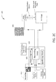
- FIGS. 2B-2C illustrate example methods to manufacture a master for fabricating an optical product in accordance with certain embodiments described herein.
- FIGS. 3A-3B illustrate example 2D data files in accordance with certain embodiments disclosed herein.
- FIGS. 3C-3D illustrate example features on a data file and the corresponding features on the surface of a master for fabricating an optical product in accordance with certain embodiments disclosed herein.
- FIG. 4A illustrates another example 2D data file in accordance with certain embodiments disclosed herein.
- FIG. 4B illustrates an example normal map used to generate the data file shown in FIG. 4A .
- FIG. 4C illustrates the 3D image reproduced by an optical product generated from a master produced using the data file shown in FIG. 4A .
- a master e.g., a master and/or daughter shim
- the optical product when illuminated, can reproduce an overt 3D image (e.g., an image that appears 3D to the naked eye) of a 3D object.
- the reflective surface of various embodiments of the optical product can produce a brighter mirror-like image produced by reflecting (or refracting) light incident on the surface.
- the surface normals of the 3D object are mimicked as surface relief on the master and/or optical product.
- the surface relief on the master and/or optical product can be thinner than the 3D object, yet produce the same appearance of the 3D object.
- the optical product can advantageously be used in applications for flexible packaging, brand identification, tamper evident containers, currency (e.g., a banknote), decoding messages, authenticity, and security, etc.
- Some security applications include incorporation of small detailed features, incorporation of non-symmetrical features, incorporation of machine readable features, etc.
- the optical product can be incorporated into an item as an embedded feature, a hot stamp feature, a windowed thread feature, or a transparent window feature.
- the optical product can be a patch, a window, or a thread.
- the optical product can have a thickness of less than 30 ⁇ m, less than 25 ⁇ m, or less than 15 ⁇ m.
- the image can appear 3D by the naked eye.
- the image can be seen at a viewing angle between 20 degrees to 160 degrees, between 15 degrees to 165 degrees, between 10 degrees to 170 degrees, between 5 degrees to 175 degrees, or between 0 degrees to 180 degrees relative to the plane of the item (e.g., relative to the banknote plane) as the item is tilted.
- the image can be viewable within one or more of these viewing angle ranges relative to the plane of the item.
- the image can be seen at a viewing angle between 20 degrees to 90 degrees, between 15 degrees to 90 degrees, between 10 degrees to 90 degrees, between 5 degrees to 90 degrees, or between 0 degrees to 90 degrees relative to the normal of the item as the item is rotated the normal of the item (e.g., in the plane of the item).
- the image can be viewable and/or visible within one or more of these viewing angle ranges as the item is rotated (e.g., rotated at least throughout the range of 90 degrees, rotated at least throughout the range of 180 degrees, rotated at least throughout the range of 270 degrees, or rotated at least throughout the range of 360 degrees) about the normal of the item (e.g., in the plane of the item).
- FIG. 1A schematically illustrates an example master 10 for fabricating an optical product 10 ′ in accordance with certain embodiments described herein.
- the master 10 can include a first surface 11 and a second surface 12 opposite the first surface 11 .
- the second surface 12 can include a plurality of portions P 1 , P 2 , . . . P n .
- Each portion P n can correspond to a plurality of portions P′ 1 , P′ 2 , . . . P′ n on the optical product 10 ′.
- each portion P′ n on the optical product 10 ′ can also be referred to as a cell, pixel, or a tile.
- Each portion P′ n can have a length between 30 ⁇ m and 100 ⁇ m, between 35 ⁇ m and 55 ⁇ m, or between 40 ⁇ m and 50 ⁇ m.
- Each portion P′ n can have a width between 30 ⁇ m and 100 ⁇ m, between 35 ⁇ m and 55 ⁇ m, or between 40 ⁇ m and 50 ⁇ m. Accordingly, in various embodiments, the aspect ratio of each portion P′ n can be 1:1 or 1:1.1.
- Each portion P n of the master 10 (and each portion P′ n of the optical product 10 ′) can correspond to a point S 1 , S 2 , . . . S n on a surface S of the 3D object 50 .
- Each portion P n can include features F 1 , F 2 , . . . F n corresponding to elements E 1 , E 2 , . . . E n , e.g., non-holographic elements, on the optical product 10 ′.
- a gradient (e.g., slope) in the features F 1 , F 2 , . . .
- F n can correlate to an inclination (e.g., slope) of the surface S of the 3D object 50 at the corresponding point S 1 , S 2 , . . . S n .
- an orientation of the features F 1 , F 2 , . . . F n can correlate to an orientation of the surface S of the 3D object 50 at the corresponding point S 1 , S 2 , . . . S n .
- an optical product 10 ′ fabricated using the example master 10 can be configured, when illuminated, to reproduce by reflected (or refracted) light, a 3D image 50 ′ (e.g., an image that appears 3D) of at least a part of a 3D object 50 .
- the image can be observed by the naked eye and under various lighting conditions (e.g., specular, diffuse, and/or low light conditions).
- the optical product 10 ′ can be used on a variety of products to reproduce a 3D image 50 ′ of at least a part of a 3D object 50 .
- the optical product 10 ′ can be placed on decorative signs, advertisements, labels (e.g., self-adhesive labels), packaging (e.g., consumer paper board packaging and/or flexible packaging), consumer goods, collectible cards (e.g., baseball cards), etc.
- the optical product 10 ′ can also be advantageously used for authenticity and security applications.
- the optical product 10 ′ can be placed on currency (e.g., a banknote), credit cards, debit cards, passports, driver's licenses, identification cards, documents, tamper evident containers and packaging, bottles of pharmaceuticals, etc.
- the optical product 10 ′ can be a reflective or transmissive device.
- the optical product 10 ′ can include reflective material (e.g., reflective metal such as aluminum, copper, or silver disposed on the plurality of elements E 1 , E 2 , . . . E n , or a transparent, relatively high refractive index material such as ZnS or TiO 2 disposed on the plurality of elements E 1 , E 2 , . . . E n creating a semi-transmitting/partially reflective boundary).
- the optical product 10 ′ can be reflective or transmissive.
- the optical product 10 ′ can be partially reflective or partially transmissive. The thickness of the reflective material at which the optical product 10 ′ is reflective or transmissive can depend on the chemical composition of the reflective material.
- the optical product 10 ′ can include a reflective surface 12 ′ from which light can reflect from the elements E 1 , E 2 , . . . E n to reproduce the image 50 ′ of the 3D object 50 or at least part of the 3D object 50 .
- the optical product 10 ′ can be made of a reflective metal (e.g., aluminum, copper, or silver), a semi-transparent metal, or a material (e.g., polymer, ceramic, or glass) coated with a reflective metal. Reflective coatings that employ non-metallic material can also be employed.
- the thickness of the coating layer can be greater than or equal to 40 nm such that the layer is opaque.
- the thickness of the reflective metal can be less than 40 nm such that the layer is semi-transparent (e.g., 30% transparent 40% transparent, 50% transparent, 60% transparent, 70% transparent, or any ranges inbetween these values, etc.).
- the elements E 1 , E 2 , . . . E n can reflect light towards or away from the observer's eye to reproduce the image 50 ′ the 3D object 50 .
- E n can reflect light towards the observer's eye in bright areas, and reflect light away from the observer's eye in dark areas.
- the slopes of the elements E n can be configured to create the 3D depth perception of the image. For example, elements E n with less steep slopes can cause light to reflect toward the observer's eye creating more brightness, while elements E n with steeper slopes can cause light to reflect away from the observer's eye creating more darkness.
- the optical product 10 ′ can include a layer (e.g., a coating) of a transparent, relatively high refractive index material such as, for example, ZnS or TiO 2 .
- a transparent, relatively high refractive index material such as, for example, ZnS or TiO 2 .
- light can transmit through the material and can also reflect at each of the elements E 1 , E 2 , . . . E n due to the presence of the relatively high index layer which can create index mismatch and results in Fresnel reflection.
- the relatively high index material can be up to a full visible wavelength in thickness in some embodiments. If a color tint is used, the relatively high index material can be up to a 1 ⁇ 4 of a visible wavelength in thickness in some embodiments.
- the optical product 10 ′ can include a protective covering, e.g., an organic resin, to protect the elements E 1 , E 2 , . . . E n and/or any coating layer from corrosion from acidic or basic solutions or organic solvents such as gasoline and ethyl acetate or butyl acetate.
- the protective covering can also provide protection during subsequent processing steps and use of the optical product 10 ′ (e.g., during the manufacturing of currency and/or by general handling by the public).
- the optical product 10 ′ can be placed on or in another surface (e.g., as an embedded feature, a hot stamped feature such as a patch, a windowed thread feature, or a transparent window feature).
- the optical product 10 ′ can be placed under another surface (e.g., laminated under a film and/or cast cured).
- the optical product 10 ′ can be placed between two other surfaces (e.g., hot stamped on another surface and laminated under a film). Additional features associated with the optical product 10 ′ will become apparent with the disclosure herein of the master 10 for fabricating the optical product 10 ′.
- the image 50 ′ of at least part of the 3D object 50 can be reproduced when the optical product 10 ′ is illuminated.
- the image 50 ′ can be reproduced by a multitude of relatively small mirrors (e.g., each of the elements E 1 , E 2 , . . . E n having both a length and width between 30 ⁇ m and 100 ⁇ m, between 35 ⁇ m and 55 ⁇ m, or between 40 ⁇ m and 50 ⁇ m) which can be curved (e.g., have a freeform curvature) or planar.
- a reflective surface of the optical product 10 ′ can provide a surface for specular reflection, such that the image 50 ′ can be produced by the reflected light (e.g., like a mirror). Accordingly, various embodiments can produce a bright, high quality image. Some embodiments can also utilize techniques for producing diffuse reflection, e.g., for special or desired effects. Furthermore, the image 50 ′ can be a substantially similar reproduction (e.g., with similar details), an approximate reproduction (e.g., with less details), and/or a scaled copy (e.g., scaled up or down in size) of the 3D object 50 or part of the 3D object 50 .
- the 3D object 50 to be reproduced is not particularly limited and can advantageously include rotationally non-symmetrical and/or irregularly shaped objects, as well as symmetrical and/or regularly shaped objects.
- the 3D object 50 can include one or more alphanumeric characters and/or symbols.
- the 3D object 50 can include one or more text, one or more alphabetic characters, one or more numeric characters, one or more letters, one or more numbers, one or more symbols, one or more punctuation marks, one or more mathematical operators, etc.
- the 3D object 50 can also include one or more graphical images or logos, e.g., a company logo, a team logo, product branding designs, etc.
- the 3D object 50 can include irregularly shaped features in addition to planar and curved features.
- the 3D object 50 can comprise animals, humans, plants or trees, landscapes, buildings, cars, boats, airplanes, bicycles, furniture, office equipment, sports equipment, foods, drinks, personal care items, flags, emblems, symbols like country, company or product symbols including trademarks, or parts thereof or groups or combination of these items with or without other items.
- the objects may be cartoon or artistic renditions. A wide range of other objects are possible.
- the image 50 ′ can be seen at various viewing angles (e.g., between 20 degrees to 160 degrees, between 15 degrees to 165 degrees, between 10 degrees to 170 degrees, between 5 degrees to 175 degrees, or between 0 degrees to 180 degrees relative to the plane of the item (e.g., relative to the banknote plane).
- various viewing angles e.g., between 20 degrees to 160 degrees, between 15 degrees to 165 degrees, between 10 degrees to 170 degrees, between 5 degrees to 175 degrees, or between 0 degrees to 180 degrees relative to the plane of the item (e.g., relative to the banknote plane).
- different sets of elements E 1 , E 2 , . . . E n can be seen by the observer to provide the different images of the 3D object.
- the image can be seen at a viewing angle between 20 degrees to 90 degrees, between 15 degrees to 90 degrees, between 10 degrees to 90 degrees, between 5 degrees to 90 degrees, or between 0 degrees to 90 degrees relative to the normal of the item as the item is rotated about the normal of the item.
- the image can be viewable within one or more of these viewing angle ranges as the item is rotated (e.g., rotated at least throughout the range of 90 degrees, rotated at least throughout the range of 180 degrees, rotated at least throughout the range of 270 degrees, or rotated at least throughout the range of 360 degrees) about the normal of the item.
- the image 50 ′ can be substantially without iridescence or change in color with angle.
- the size of the portions P′ 1 , P′ 2 , . . . P′ n can have a length and width between 30 ⁇ m and 100 ⁇ m, between 35 ⁇ m and 55 ⁇ m, or between 40 ⁇ m and 50 ⁇ m.
- the portions P′ n may be small enough such that the portions P′ n are not resolvable by a human observer under normal viewing conditions (e.g., a reading distance of 18 to 24 inches between the eye and the item to be viewed).
- the portions P′ n may be big enough such that the cone of light passing through the pupil (e.g., 5 mm in diameter) is small enough such that the eye may see a majority of the colors mixed as white light at a distance of 18-24 inches.
- a majority e.g., greater than 50%, greater than 55%, greater than 60%, greater than 65%, greater than 70%, greater than 80%, greater than 90%, and any ranges in between these values
- a majority e.g., greater than 50%, greater than 55%, greater than 60%, greater than 65%, greater than 70%, greater than 80%, greater than 90%, and any ranges in between these values
- the plurality of portions P′ 1 , P′ 2 , . . . P′ n on the optical product 10 ′ can include a single non-holographic element E 1 (as opposed to a plurality of spaced apart non-holographic elements E n that may resemble a grating-like feature).
- grating-like features can cause light to be dispersed with some of the light collected by the pupil of the eye.
- the light captured by the pupil may appear as a color. Accordingly, in various embodiments of the optical product 10 ′ that have a majority of the plurality of portions P′ 1 , P′ 2 , . . . P′ n having not more than a single non-holographic reflective or refractive element E 1 , unwanted color caused by grating-like features may possibly be substantially reduced and/or eliminated. Similarly, color change with angle of tilt can be reduced. In some embodiments, at least 20%, at least 30%, at least 40%, at least 50%, at least 60%, at least 70%, at least 80%, at least 90%, or any ranges in between these values) of the plurality of portions P′ 1 , P′ 2 , .
- the optical product 10 ′ can include a single non-holographic element E 1 .
- the single element may be slowly varying and/or substantially flat.
- the maximum average slope per portion with a single feature is less than 1 ⁇ 2, less than 1 ⁇ 3, less than 1 ⁇ 4, less than 1 ⁇ 5, less than 1 ⁇ 6, potentially flat, and any ranges in between these values depending on feature height and width.
- the elements E n can be discontinuous and/or having different orientation with non-holographic elements E 1 , E 2 , . . . E n in surrounding adjacent portions P′ n .
- the discontinuity and/or different orientations between grating-like features can cause a lateral shift of the grating-like feature.
- the lateral shift may cause the color spectrum to shift as well (e.g., from red to blue to green). The colors may combine on the retina providing an average white irradiance distribution.
- certain embodiments of the optical product 10 ′ can utilize a certain portion P′ n size, a single non-holographic element E 1 in a portion P′ n , discontinuous and/or differently orientated elements E n to produce images that may be substantially without iridescence or change in color with angle.
- the application of these features can be dependent on the image to be formed.
- the optical product 10 ′ can include surfaces which additionally include features from which light can diffract, e.g., at surface defects, at discontinuities at borders, and/or via incorporation of diffractive or holographic elements.
- diffractive or holographic features can be combined with the surface features disclosed herein that produce an image of a 3D object using reflection (or possibly refraction, e.g., in transmission) without relying on diffraction.
- the master 10 can be either a negative or positive master. Whether as a negative or positive master, the method to produce the master 10 is not particularly limited.
- the features F 1 , F 2 , . . . F n on surface 12 of the master 10 can be produced using any technique known in the art or yet to be developed, including but not limited to photolithography (e.g., UV or visible light), electron beam lithography, and ion beam lithography to name a few.
- the materials that can be used to manufacture the master 10 are not particularly limited and can include glasses, ceramics, polymers, metals, etc.
- the master 10 can form a surface 12 ′ of the optical product 10 ′ that is complementary to the surface 12 of the master 10 .
- the features F 1 , F 2 , . . . F n on the surface 12 of the master 10 can be the inverse of the elements E 1 , E 2 , . . . E n on the surface 12 ′ of the optical product 10 ′.
- the master 10 can be used to form the optical product 10 ′.
- the master 10 can be used to emboss the elements E 1 , E 2 , . . .
- E n onto a metal sheet, a polymeric substrate such as a thermoformable polymer, or a UV curable photoresist layer such as a UV curable resin, or to injection mold the elements E 1 , E 2 , . . . E n onto a polymer.
- a polymeric substrate such as a thermoformable polymer, or a UV curable photoresist layer such as a UV curable resin
- the master 10 can provide a surface 12 ′ for the optical product 10 ′ that is substantially similar to the surface 12 of the master 10 .
- the features F 1 , F 2 , . . . F n on the surface 12 of the master 10 can be substantially similar to the elements E 1 , E 2 , . . . E n on the surface 12 ′ of the optical product 10 ′.
- the positive master 10 can provide a model for the optical product 10 ′.
- the positive master 10 can be used to create an inverse image of the 3D object 50 .
- the positive master 10 can be used to fabricate one or more negative masters.
- the master 10 is shown producing a product directly, in certain embodiments the master 10 is employed to produce one or more other masters (e.g., daughter shims) or intermediate surfaces that can in turn be used to produce a product.
- a first negative master can be used to produce a second master that is a positive master.
- the second positive master can be used to make a third negative master.
- the third negative master can be used to produce a fourth positive master.
- the fourth positive master can be used to produce a product.
- a tooling tree of masters e.g., four, five, six, etc. generations deep) can be produced.
- Certain embodiments of the optical product 10 ′ disclosed herein can be advantageously manufactured on a large industrial scale. Some embodiments can be manufactured by embossing the elements E 1 , E 2 , . . . E n into an UltraViolet (UV) curable resin coated onto various polymeric substrates, such as, for example, polyethylene terephthalate (PET), oriented polypropylene (OPP), low density polyethylene (LDPE), linear low density polyethylene (LLDPE), polypropylene (PP), polyvinyl chloride (PVC) polycarbonate (PC) or any other type of plastic film or carrier.
- UV UltraViolet
- PVC polyvinyl chloride
- PC polycarbonate
- thermoformable plastics such as PVC and PC, the elements E 1 , E 2 , . . .
- E n can be embossed directly into the substrate without the UV curable layer.
- the polymeric substrate can be clear.
- the polymeric substrates can have a thickness less than or equal to 30 microns, less than or equal to 25 microns, or less than or equal to 15 microns.
- Some such polymeric substrates having elements E 1 , E 2 , . . . E n can be formed into security threads that can be incorporated into a banknote having a paper thickness of 100 microns.
- the master 10 can include a first surface 11 and a second surface 12 .
- the first surface 11 is shown for simplicity as a planar surface. However, the shape of the first surface 11 is not particularly limited.
- the second surface 12 can be opposite the first surface 11 .
- the second surface 12 can include a plurality of portions P 1 , P 2 , . . . P n .
- the plurality of portions P 1 , P 2 , . . . P n can form a single cell (e.g., a mono-cell).
- the plurality of portions P 1 , P 2 , . . . P n can form a plurality of cells.
- each of the plurality of portions P 1 , P 2 , . . . P n can form a cell of the plurality of cells.
- the number of cells is not particularly limited and can depend on factors such as size and resolution of the image to be reproduced.
- the portions P 1 , P 2 , . . . P n can form a pixelated surface.
- FIG. 1A only one row of portions P 1 , P 2 , . . . P n is shown in FIG. 1A .
- certain embodiments can include additional rows and columns of portions P 1 , P 2 , . . . P n .
- FIG. 1B the portions P 1 , P 2 , . . .
- P n can include a plurality of rows and columns spanning across the surface 12 of the master 10 .
- first row is labeled as P 1 , P 2 , . . . P n .
- FIG. 1B shows a 4 ⁇ 4 array of portions P 1 , P 2 , . . . P n , the numbers of rows, columns, and portions P 1 , P 2 , . . . P n are not particularly limited.
- borders 13 can surround at least part of the portions P 1 , P 2 , . . . P n .
- the borders 13 can substantially surround a portion P n , or can surround just part of a portion P n .
- discontinuities can extend around all or substantially all of the portion P n .
- discontinuities may extend on just a part of the portion P n .
- the borders 13 can help define the size and shape of the portions P 1 , P 2 , . . . P n in some embodiments.
- the size and shape of the portions P 1 , P 2 , . . . P n are not particularly limited.
- some of the portions P 1 , P 2 , . . . P n can comprise a symmetrical shape.
- the symmetrical shape can include a rectangle, a square, a rhombus, an equilateral triangle, an isosceles triangle, a regular polygon (e.g., a regular pentagon, a regular hexagon, a regular octagon, etc.), to name a few.
- the symmetrical shape can also include curvature, e.g., a circle, an ellipse, etc.
- P n can comprise a non-symmetrical shape, e.g., a non-rotationally symmetrical shape, and/or an irregular shape.
- some of the portions P 1 , P 2 , . . . P n can have a shape that is substantially the same as other portions P 1 , P 2 , . . . P n .
- at least 20%, at least 30%, at least 40%, at least 50%, at least 60%, at least 70%, at least 80%, at least 90% (or any range in between these percentages) of the portions P 1 , P 2 , . . . P n can have the same shape, size, or both.
- some of the portions P 1 , P 2 , . . . P n can have a shape that is different from other portions P 1 , P 2 , . . . P n .
- Arrangement of the portions P 1 , P 2 , . . . P n is not particularly limited. For example, whether with or without borders, whether symmetrically shaped or non-symmetrically shaped, or whether regularly or irregularly shaped, the portions P 1 , P 2 , . . . P n can form a periodic array. In other embodiments, whether with or without borders, whether symmetrically shaped or non-symmetrically shaped, or whether regularly or irregularly shaped, the portions P 1 , P 2 , . . . P n can form an aperiodic array. In yet other embodiments, the portions P 1 , P 2 , . . . P n can form a combination of periodic and aperiodic arrays.
- each portion P n can correspond to a point S 1 , S 2 , . . . S n on the surface S of the 3D object 50 , and each portion P n can include one or more features F 1 , F 2 , . . . F n .
- the features F 1 , F 2 , . . . F n shown in FIG. 1A appear linear and substantially similar to each other.
- the features F 1 , F 2 , . . . F n can vary in number, size, shape, and orientation.
- the features F 1 , F 2 , . . . F n can include linear and/or curved features, for example as seen from a top or front view.
- the features F 1 , F 2 , . . . F n can include facets, such as linear or curved saw tooth shaped features.
- the size of the features F 1 , F 2 , . . . F n are not particularly limited. However, from a manufacturing and economic perspective, in some embodiments, a smaller height (e.g., 0 ⁇ m to 10 ⁇ m) can be advantageous to reduce the amount of material used. Accordingly, in some embodiments, the heights of the features F 1 , F 2 , . . .
- F n can be from close to 0 ⁇ m to 0.1 ⁇ m (e.g., 0 nm to 100 nm, 1 nm to 75 nm, or 1 nm to 50 nm), from close to 0 ⁇ m to 1 ⁇ m (e.g., 0 nm to 1000 nm, or 1 nm to 500 nm), from close to 0 ⁇ m to 5 ⁇ m (e.g., 1 nm to 5 ⁇ m, 10 nm to 5 ⁇ m, 50 nm to 5 ⁇ m, 75 nm to 5 ⁇ m, 0.1 ⁇ m to 5 ⁇ m, 0.5 ⁇ m to 5 ⁇ m, or 1 ⁇ m to 5 ⁇ m), or from close to 0 ⁇ m to 8 ⁇ m (e.g., 1 nm to 8 ⁇ m, 10 nm to 8 ⁇ m, 50 nm to 8 ⁇ m, 75 nm to 8 ⁇ m, 0.1 ⁇
- the heights of the features F 1 , F 2 , . . . F n can go up to 15 ⁇ m, up to 20 ⁇ m, up to 25 ⁇ m, or any ranges from 1 ⁇ m, 2 ⁇ m, or 3 ⁇ m up to 25 ⁇ m. In yet other embodiments, the heights of the features F 1 , F 2 , . . . F n can go up to 50 m if needed, e.g., depending on the desired size of the 3D image to be reproduced.
- the lateral dimensions of the features F 1 , F 2 , . . . F n are not particularly limited, but can depend on the details of the 3D object.
- the lateral dimensions of the features F 1 , F 2 , . . . F n can be less than 1 ⁇ m. Accordingly, the lateral dimensions of the features F 1 , F 2 , . . .
- F n can be from close to 0 ⁇ m to 0.1 ⁇ m (e.g., 0 nm to 100 nm, 1 nm to 75 nm, or 1 nm to 50 nm), from close to 0 ⁇ m to 1 ⁇ m (e.g., 0 nm to 1000 nm, or 1 nm to 500 nm), from close to 0 ⁇ m to 5 ⁇ m (e.g., 1 nm to 5 ⁇ m, 10 nm to 5 ⁇ m, 50 nm to 5 ⁇ m, 75 nm to 5 ⁇ m, 0.1 ⁇ m to 5 ⁇ m, 0.5 ⁇ m to 5 ⁇ m, or 1 ⁇ m to 5 ⁇ m), or from close to 0 ⁇ m to 8 ⁇ m (e.g., 1 nm to 8 ⁇ m, 10 nm to 8 ⁇ m, 50 nm to 8 ⁇ m, 75 nm to 8 ⁇ m, 0.1 ⁇
- a lateral distance between two features can be defined in some embodiments as a pitch.
- the pitch between features within a portion P n can be substantially the same within the portion P n .
- the feature F 1 in portion P 1 of the portions P 1 , P 2 , . . . P n , the feature F 1 can comprise a plurality of features that form a periodic array such that the pitch is substantially the same within portion P 1 .
- P n can form a periodic array such that the pitch is substantially the same among the portions P 1 , P 2 , . . . P n .
- the features could be chirped and form an aperiodic array such that the pitch may be different among multiple portions P 1 , P 2 , . . . P n .
- the pitch may be different for different portions P 1 , P 2 , . . .
- the pitch can be slowly varying (e.g., less than 15% change per lateral distance, less than 12% change per lateral distance, less than 10% change per lateral distance, less than 8% change per lateral distance, less than 5% change per lateral distance, less than 3% change per lateral distance, or less than 1% change per lateral distance) among the portions P 1 , P 2 , . . . P n .
- the pitch may uniformly change across multiple portions P 1 , P 2 , . . . P n .
- the features could be chirped within a portion P n such that the pitch may be different within the portion P n .
- the pitch within the portion P n may slowly vary (e.g., less than 15% change per lateral distance, less than 12% change per lateral distance, less than 10% change per lateral distance, less than 8% change per lateral distance, less than 5% change per lateral distance, less than 3% change per lateral distance, or less than 1% change per lateral distance).
- the pitch may uniformly change with the portion P n .
- the pitch in certain embodiments can be between 1 ⁇ m and 100 ⁇ m, between 1 ⁇ m and 75 ⁇ m, between 1 ⁇ m and 50 ⁇ m, or between 1 ⁇ m and 25 ⁇ m.
- the features F 1 , F 2 , . . . F n can correspond to elements E 1 , E 2 , . . . E n on the optical product 10 ′, and since the optical product 10 ′ is configured to reproduce the 3D object 50 , aspects of the features F 1 , F 2 , . . . F n can correlate to aspects of the surface S of the 3D object 50 at the corresponding point S 1 , S 2 , . . . S n . For example, a gradient (e.g., slope) in the features F 1 , F 2 , . . .
- each feature can include a slope.
- a slope of the feature F 1 can correlate to the inclination of the surface S of the 3D object 50 at the corresponding point S 1 .
- the slope of the feature F 1 can correlate to the polar angle ⁇ 1 from reference line R 1 of the 3D object 50 . Accordingly, the slopes of the features F 1 , F 2 , . . . F n can mimic the surface normals of the 3D object 50 .
- Various embodiments can advantageously have a uniform gradient (e.g., uniform slope) within each portion P n such that the gradient is a single value (e.g., a single polar angle ⁇ n ) at the corresponding point S n on the surface S of the 3D object 50 .
- the feature F n within a portion P n includes a plurality of features, and the features within the portion P n may have more than one gradient (e.g., different slopes).
- the average gradient (e.g., average slope) of the features within the portion P n can correlate to the inclination of the surface S of the 3D object 50 at the corresponding point S n .
- varying the slopes within and/or among portions P 1 , P 2 , . . . P n can create contrast on the surface and therefore, on the image 50 ′. Furthermore, varying at least one of the height of features, pitch between features (e.g., lateral distance between two features), and slope of the features in one or more portions P 1 , P 2 , . . . P n can be used in authenticity and security applications. For example, one can intentionally vary the pitch within one or more portions P n , but maintain the given slopes. The image 50 ′ of the 3D object 50 would be reproduced, yet upon closer inspection of the presence of the intentional variation within one or more portions P 1 , P 2 , . . . P n , authenticity can be verified. Other variations are possible.
- the orientation of features F 1 , F 2 , . . . F n can correlate to an orientation of the surface S of the 3D object 50 at the corresponding point S 1 , S 2 , . . . S n .
- an orientation of the feature F 1 can correlate to the orientation of the surface S of the 3D object 50 at the corresponding point S 1 .
- the orientation of the feature F 1 can correlate to the azimuth angle ⁇ 1 from reference line R 2 of the 3D object 50 .
- Various embodiments can advantageously have a uniform orientation within each portion P n , such that the orientation is a single value (e.g., a single azimuth angle (P n ) at the corresponding point S n on the surface S of the 3D object 50 .
- the feature F n within a portion P n includes a plurality of features, and the features within the portion P n may have more than one orientation (e.g., different orientations).
- the average orientation of the features within the portion P n can correlate to the orientation of the surface S of the 3D object 50 at the corresponding point S n .
- P n can slowly vary (e.g., less than 15% change per lateral distance, less than 12% change per lateral distance, less than 10% change per lateral distance, less than 8% change per lateral distance, less than 5% change per lateral distance, less than 3% change per lateral distance, or less than 1% change per lateral distance) within and among the portions P 1 , P 2 , . . . P n .
- a feature F 1 includes multiple features within a portion
- the features can appear discontinuous with other features within the portion.
- the features F 1 , F 2 , . . . F n can appear discontinuous with features in surrounding adjacent portions.
- the portions P 1 , P 2 , . . . P n can form a single cell or a mono-cell.
- the features F 1 , F 2 , . . . F n can appear continuous and smoothly varying depending on the shape.
- the features F 1 , F 2 , . . . F n can appear discontinuous due to discontinuities in the 3D object 50 .
- the features F 1 , F 2 , . . . F n can comprise linear features corresponding to a substantially smooth region of the surface S of the 3D object 50 .
- the features F 1 , F 2 , . . . F n can also comprise non-linear features, e.g., curved features as seen from a top or front view, corresponding to a curved region of the surface S of the 3D object 50 , e.g., instead of flat facets.
- features F 1 , F 2 , . . . F n that are linear can be used to correspond to a curved region of the surface S of the 3D object 50 .
- linear features on a master 10 can be used to represent a curved region by using a piecewise approximation function (e.g., a piecewise linear function such as a function comprising straight line sections).
- features F 1 , F 2 , . . . F n that are non-linear can be used to correspond to a substantially smooth region of the surface S of the 3D object 50 .
- non-linear features on a master 10 can be used to represent smooth regions on the surface S of the 3D object because the features F 1 , F 2 , . . . F n can correspond to relatively small sized features on the optical product 10 ′.
- the pitch and/or texture on the optical product 10 ′ can be between 1 ⁇ m and 100 ⁇ m, between about 1 ⁇ m and about 75 ⁇ m, between about 1 ⁇ m and about 50 ⁇ m, or between about 1 ⁇ m and about 25 ⁇ m.
- the features F 1 , F 2 , . . . F n can correspond to aspects of the surface S of the 3D object 50 and can also correspond to elements E 1 , E 2 , . . . E n on the optical product 10 ′ such that the optical product 10 ′ can reproduce an image 50 ′ of the 3D object 50 .
- the elements E 1 , E 2 , . . . E n on the optical product 10 ′ can be non-holographic.
- the features F 1 , F 2 , . . . F n on the surface 12 of the master 10 can include non-sinusoidal features or non-quasi-sinusoidal features.
- sinusoidal or quasi-sinusoidal features can be diffractive with +/ ⁇ orders of equal intensity that generate a twin image.
- One positive order and one negative order can share the incident light and result in a simultaneous twin image with counter-intuitive movement of one image with respect to the other.
- Such effects may be non-ideal.
- the features F 1 , F 2 , . . . F n on the surface 12 of the master 10 can include other shapes, such as saw toothed shapes as described herein.
- some embodiments described herein do not necessarily rely on holography to reproduce an image, some embodiments can include diffractive or holographic features (e.g., less than about 50% of the surface area, less than about 40% of the surface area, less than about 30% of the surface area, less than about 20% of the surface area, less than about 10% of the surface area, less than about 5% of the surface area, less than about 3% of the surface area, less than about 2% of the surface area, or less than about 1% of the surface area) to be used in conjunction with the non-holographic elements E 1 , E 2 , . . . E n described herein.
- diffractive or holographic features e.g., less than about 50% of the surface area, less than about 40% of the surface area, less than about 30% of the surface area, less than about 20% of the surface area, less than about 10% of the surface area, less than about 5% of the surface area, less than about 3% of the surface area, less than about 2% of the surface area, or less than about
- the second surface 12 of the master 10 can further comprise features corresponding to holographic elements on the optical product 10 ′ in one or more portions P 1 , P 2 , . . . P n .
- a holographic layer can be added over or under the surface 12 ′ of the optical product 10 ′.
- FIG. 1D is another example optical product 10 ′ in accordance with certain embodiments described herein.
- the optical product 10 ′ can include a plurality of portions P′ 1 , P′ 2 , . . . P′ n .
- Each portion P′ n can include elements E 1 , E 2 , . . . E n , e.g., non-holographic elements, on the optical product 10 ′.
- the elements E 1 , E 2 , . . . E n can be embossed on the bottom surface of the substrate, e.g. UV curable resin having a refractive index of 1.5.
- E n can be coated with a reflective coating.
- the elements E 1 , E 2 , . . . E n may then be embedded between the substrate and the item to which the optical product 10 ′ is attached.
- the slopes of the elements E 1 , E 2 , . . . E n can be configured to create the 3D depth perception of the image. For example, elements E 1 , E 2 , . . . E n with less steep slopes can cause light to reflect toward the observer's eye creating more brightness, while elements E 1 , E 2 , . . . E n with steeper slopes can cause light to reflect away from the observer's eye creating more darkness.
- elements E 1 , E 2 , . . . E n with steep enough slopes can cause light to be totally internally reflected within the substrate (which has a higher index than the surrounding medium), and creating even more darkness.
- FIG. 1E is another example optical product 10 ′ in accordance with certain embodiments described herein.
- the optical product 10 ′ can include a plurality of portions P′ 1 , P′ 2 , . . . P′ n .
- Each portion P′ n can include elements E 1 , E 2 , . . . E n , e.g., non-holographic elements, on the optical product 10 ′.
- utilizing embodiments of the optical product 10 ′ having elements E 1 , E 2 , . . . E n (or masters having features F 1 , F 2 , . . . F n ) with smaller height can be advantageous to reduce the amount of material used.
- certain embodiments can utilize elements E 1 , E 2 , . . . E n with slowly varying surfaces (e.g., slopes) creating a substantially contiguous surface from one portion P′ n to another.
- the number of substantially contiguous portions can include at least two, three, four, five, eight, ten, fifteen, twenty, or more, or be in any range in between these values.
- FIG. 2 An example method 100 is shown in FIG. 2 .
- the method 100 can include providing a data file, e.g., a 2D data file, configured to describe, characterize, and/or record features the 3D object and/or 3D image 50 ′.
- the data file can provide the pattern of the features F 1 , F 2 , . . . F n on the surface 12 of the master 10 .
- the data file can comprise a plurality of portions (as will be described further herein).
- Each portion can correspond to one or more points on a surface S of the 3D object 50 .
- Each portion can comprise features of intensity corresponding to non-holographic elements on the optical product 10 ′.
- a gradient in intensity can correlate to an inclination of the surface S of the 3D object 50 at the one or more corresponding points.
- an orientation of the features can correlate to an orientation of the surface S of the 3D object 50 at the one or more corresponding points.
- the method 100 can further include manufacturing the master 10 based at least in part on the 2D data file.
- FIG. 2A illustrates an example method that can be used to manufacture a surface relief diffuser and also to determine a height displacement file used to manufacture the diffuser.
- an input image 210 of the 3D object 50 e.g., a 2D photograph of the 3D object
- the recording loop 220 of the main program 225 of the processor 230 is entered into the recording loop 220 of the main program 225 of the processor 230 .
- the processor 230 can produce a height displacement file 240 that is configured to describe the intensities of the 3D object 50 .
- This height displacement file 240 can be used as a map to generate the pattern of the diffuser.
- the intensities of the 3D object can be correlated to a depth for the diffuser.
- the black sections of the 3D object 50 can correlate to the surface of the diffuser, white sections of the 3D object 50 can correlate to a lower depth (e.g., down 10 ⁇ m), and grey sections of the 3D object 50 can correlate to some depth in between.
- a lower depth e.g., down 10 ⁇ m
- grey sections of the 3D object 50 can correlate to some depth in between.
- Other variations are possible.
- a digital micromirror device (DMD) video projector 250 can be used along with the photoresist recording plate 260 , each receiving the inputted information from the recording loop 220 .
- the DMD video projector 250 includes a DMD chip that includes a plurality of micromirrors that in certain embodiments can correspond to the pixels of the height displacement file 240 .
- the pixels of the height displacement file 240 can also correspond to the regions on the X-Y stage of the photoresist recording plate 260 in some embodiments.
- Each micromirror of the DMD chip can be used as a spatial light modulator that, for example, reflects light from a light source in the video projector 250 in the on-state, and that does not reflect light in the off-state. Varying the amount of light intensity can be produced by varying the time the micromirror is in the on- and off-states (e.g., pulse width modulation, etc.).
- demagnification optics 255 can be used to produce the pattern of the diffuser in a light sensitive material, e.g., a photoresist, on the resist recording plate 260 .
- the resist can be used as the diffuser.
- the diffuser can be used with certain embodiments of the optical product 10 ′ to produce a diffuse or hazy layer over the reflected image 50 ′ to produce an image with a matte finish.
- FIG. 2B illustrates an example method that can be used to manufacture the master 10 and also to determine the data file to be used to manufacture the master 10 , e.g., to determine the pattern of the features F 1 , F 2 , . . . F n on the surface 12 of the master 10 .
- Certain such embodiments can be advantageous as a 3D physical object and/or a 3D model utilizing physical dimensions of the 3D object (e.g., topographical calculations) are not required.
- the input image 305 can be a 2D input image (e.g., a 2D photograph of the 3D object) or 2D image converted from a 3D image.
- the input image 305 can be converted into a 2D interpolated image 308 and produced as a 2D converted image 310 .
- the 2D image of the 3D object can be translated into a gray scale image (e.g., a normal map 315 wherein black, white, and gray regions correlate to different heights of the 3D object).
- the converted image 310 (or a normal map 315 ) is entered into the recording loop 320 of the main program 325 of the processor 330 in accordance with certain embodiments described herein. Similar to the method 200 in FIG.
- the processor 330 can produce a data file 340 , e.g., a 2D data file, that is configured to describe the 3D image 50 ′ of at least a part of the 3D object 50 .
- the intensities in the data file 340 can be assigned based on gray scale.
- the data file 340 can comprise a plurality of portions. Each portion can correspond to one or more points on a surface S of the 3D object 50 .
- Each portion can comprise features of intensity corresponding to non-holographic elements on the optical product 10 ′.
- a gradient in intensity can correlate to a gradient or an inclination of the surface S of the 3D object 50 at the one or more corresponding points.
- an orientation of the features can correlate to an orientation of the surface S of the 3D object 50 at the one or more corresponding points.
- This data file 340 can be used as a map to generate the pattern of features F 1 , F 2 , . . . F n on the surface 12 of the master 10 .
- An example data file is discussed with respect to FIG. 3A .
- a digital micromirror device (DMD) video projector 350 can be used along with the photoresist recording plate 360 , each receiving the inputted information from the recording loop 320 .
- the plurality of micromirrors in the DMD video projector 350 in certain embodiments can correspond to the pixels of the data file 240 .
- the pixels of the data file 340 can also correspond to one or more portions P 1 , P 2 , . . . P n of the surface 12 of the master 10 in some embodiments.
- the demagnification optics 355 can be used to produce the pattern of features F 1 , F 2 , . . .
- the resist can be used as the surface 12 of the master 10 .
- other techniques such as electron beam lithography on electron sensitive material and ion beam lithography on ion sensitive material can also be used.
- the method 300 can further include adding on the master 10 features corresponding to holographic elements on the optical product 10 ′.
- an optical recording e.g., a planar optical recording
- the data file 340 can include features corresponding to holographic elements on the optical product 10 ′.
- a separate data file comprising the features of intensity corresponding to holographic elements on the optical product 10 ′ can be provided. Manufacturing the master 10 can be based at least in part on the data file 340 including features corresponding to non-holographic elements and on the data file including features corresponding to holographic elements on.
- the data file 340 including the features corresponding to non-holographic elements and the data file including the features corresponding to holographic elements can be used sequentially or simultaneously to manufacture the master 10 .
- a needle such as from an atomic force microscope, can be used to produce the features corresponding to the holographic elements on the optical product 10 ′.
- Other methods can be employed to add holographic features or elements.
- FIG. 2C illustrates yet another example method that can be used to determine the pattern of the features F 1 , F 2 , . . . F n on the surface 12 of the master 10 .
- the method 400 shown in FIG. 2C is similar to the method 300 shown in FIG. 2B except that a normal map 415 can be provided instead of the input image 310 .
- the normal map 415 can be inputted into the main program 425 of the processor 430 to produce the data file 440 .
- FIG. 3A illustrates an example 2D data file 540 in accordance with certain embodiments disclosed herein.
- the data file 540 can include a plurality of portions p 1 , p 2 , . . . p n .
- the plurality of portions p 1 , p 2 , . . . p n can form a single cell (e.g., a mono-cell).
- the plurality of portions p 1 , p 2 , . . . p n can form a plurality of cells.
- the p n can form a pixelated surface corresponding to the portions P 1 , P 2 , . . . P n of the surface 12 of the master 10 .
- the portions p 1 , p 2 , . . . p n can include a plurality of rows and columns.
- borders 13 ′ can surround at least part of the portions p 1 , p 2 , . . . p n .
- the borders 13 ′ can substantially surround a portion p n or can surround just part of a portion p n .
- the size and shape of the portions p 1 , p 2 , . . . p n on the data file 540 are not particularly limited. Some of the portions p 1 , p 2 , . . . P n can comprise a symmetrical shape.
- the symmetrical shape can include a rectangle, a square, a rhombus, an equilateral triangle, an isosceles triangle, a regular polygon (e.g., a regular pentagon, a regular hexagon, a regular octagon), etc.
- the shape can also include curvature, e.g., a circle, an ellipse, etc.
- some of the portions p 1 , p 2 , . . . P n can comprise a non-symmetrical shape, e.g., a non-rotationally symmetrical shape, and/or an irregular shape.
- 3B illustrates an example embodiment of a data file 545 with irregularly shaped portions p 1 , p 2 , . . . p n .
- some of the portions p 1 , p 2 , . . . p n can have a shape that is substantially the same as other portions p 1 , P 2 , . . . p n .
- some of the portions p 1 , p 2 , . . . p n can have a shape that is different from other portions p 1 , p 2 , . . . p n .
- the arrangement of the portions p 1 , p 2 , . . . p n in the data file 540 is not particularly limited.
- the portions p 1 , p 2 , . . . p n can form a periodic array.
- the portions p 1 , p 2 , . . . p n form a periodic array.
- the portions p 1 , p 2 , . . . p n form a periodic array.
- the portions p 1 , p 2 , . . . p n form a periodic array.
- . p n can form an aperiodic array.
- the portions p 1 , p 2 , . . . p n form an aperiodic array.
- the portions p 1 , p 2 , . . . p n can form a combination of periodic and aperiodic arrays.
- each portion p n can include features f 1 , f 2 , . . . f n that correspond to features F 1 , F 2 , . . . F n on the surface 12 of the master 10 .
- Portion p a has a single feature f 1
- portion p b has multiple features f n .
- the features f 1 , f 2 , . . . f n of the data file 540 can include features of intensity (varying dark and light lines). In some embodiments, the intensity can correlate to the height of a feature on the surface S of the 3D object 50 .
- a lateral distance between two features can be defined in some embodiments as a pitch.
- the pitch between features within a portion p n can be substantially the same within the portion p n .
- the feature f 1 in portion p 1 of the portions p 1 , p 2 , . . . p n , the feature f 1 can comprise a plurality of features that form a periodic array such that the pitch is substantially the same within portion p 1 .
- the features f 1 , f 2 , . . . f n among multiple portions p 1 , p 2 , . . . p n can form a periodic array such that the pitch is substantially the same among multiple portions p 1 , p 2 , . . . p n .
- the features can form an aperiodic array such that the pitch may be different among multiple portions p 1 , p 2 , . . . p n .
- the pitch can be slowly varying (e.g., less than 15% change per lateral distance, less than 12% change per lateral distance, less than 10% change per lateral distance, less than 8% change per lateral distance, less than 5% change per lateral distance, less than 3% change per lateral distance, or less than 1% change per lateral distance) among the portions p 1 , p 2 , . . . p n .
- the pitch may uniformly change across multiple portions p 1 , p 2 , . . . p n .
- the features could be chirped within a portion p n such that the pitch may be different within the portion p n .
- the pitch within the portion p n may slowly vary (e.g., less than 15% change per lateral distance, less than 12% change per lateral distance, less than 10% change per lateral distance, less than 8% change per lateral distance, less than 5% change per lateral distance, less than 3% change per lateral distance, or less than 1% change per lateral distance).
- FIG. 3A shows an example data file 540 with linear features where the pitch is substantially uniform within a portion P n
- FIG. 3B shows an example data file 545 with curved features where the pitch is substantially uniform within a portion p n
- FIG. 3A is also an example of features having a pitch that slowly changes (e.g., less than 10% change per lateral distance) across multiple portions p 1 , p 2 , . . . p n .
- each feature of intensity can include a slope.
- Various embodiments can advantageously have a uniform gradient (e.g., uniform slope) within each portion p n such that the gradient is a single value (e.g., a single polar angle ⁇ n ) at the corresponding point S n on the surface S of the 3D object 50 .
- the gradient in the features f 1 , f 2 , . . . f n can correlate to an inclination of the surface S of the 3D object 50 at the corresponding point S 1 , S 2 , . . . S n .
- the feature f n within a portion p n includes a plurality of features, and the features within the portion p n may have more than one gradient (e.g., different slopes).
- the average gradient (e.g., average slope) of the features within the portion p n can correlate to the inclination of the surface S of the 3D object 50 at the corresponding point S n .
- Various embodiments can also advantageously have a uniform orientation within each portion p n , such that the orientation is a single value (e.g., a single azimuth angle ⁇ n ) at the corresponding point S n on the surface S of the 3D object 50 .
- the orientation of features f 1 , f 2 , . . . f n can correlate to an orientation of the surface S of the 3D object 50 at the corresponding point S 1 , S 2 , . . . S n .
- the feature f n within a portion p n includes a plurality of features, and the features within the portion p n may have more than one orientation (e.g., different orientations).
- the average orientation of the features within the portion p n can correlate to the orientation of the surface S of the 3D object 50 at the corresponding point S n .
- the orientation of the features within and among the portions p 1 , p 2 , . . . P n can slowly vary (e.g., less than 15% change per lateral distance, less than 12% change per lateral distance, less than 10% change per lateral distance, less than 8% change per lateral distance, less than 5% change per lateral distance, less than 3% change per lateral distance, or less than 1% change per lateral distance) within and among the portions p 1 , p 2 , . . . p n .
- a feature f 1 includes multiple features within a portion
- the features can appear discontinuous with other features within the portion.
- the surface 12 of the master 10 is pixelated (e.g., having a plurality of cells)
- the features f 1 , f 2 , . . . f n can appear discontinuous with features in surrounding adjacent portions.
- some embodiments may include random discontinuities with substantially no (relatively little if any) negative impact in image reproduction. Such discontinuity can reduce iridescence.
- the features f 1 , f 2 , . . . f n can appear continuous and smoothly varying depending on the shape. In other such embodiments, the features f 1 , f 2 , . . . f n can appear discontinuous due to discontinuities in the 3D object 50 .
- the features f 1 , f 2 , . . . f n can comprise linear features corresponding to a substantially smooth region of the surface S of the 3D object 50 .
- the features f 1 , f 2 , . . . f n can be used to produce linear features F 1 , F 2 , . . . F n on the surface 12 of the master 10 .
- the features f 1 , f 2 , . . . f n can also be used to produce non-linear features F 1 , F 2 , . . . F n on the surface 12 of the master 10 .
- features f 1 , f 2 , . . . f n that are linear can be used to correspond to a curved region of the surface S of the 3D object 50 .
- linear features f 1 , f 2 , . . . f n in the data file can be used to represent a curved region by using a piecewise approximation function.
- non-linear features on the master 10 can be used. As described herein, in some such embodiments, non-linear features on the master 10 can be used to produce elements E 1 , E 2 , . . .
- the features f 1 , f 2 , . . . f n of the data file 540 correspond to aspects of the surface S of the 3D object 50
- the features f 1 , f 2 , . . . f n of the data file 540 can be used to produce the features F 1 , F 2 , . . . F n on the surface 12 of the master 10 .
- the features F 1 , F 2 , . . . F n on the surface 12 of the master 10 can be used to fabricate the elements E 1 , E 2 , . . . E n on the surface 12 ′ of the optical product 10 ′.
- the elements E 1 , E 2 , . . . E n on the optical product 10 ′ can be non-holographic.
- the elements E 1 , E 2 , . . . E n do not need to rely on holography to render a 3D image 50 ′ of the 3D object 50 .
- FIG. 4A is another example 2D data file 640 prepared in accordance with certain embodiments described herein.
- the data file 640 was generated by the normal map 650 shown in FIG. 4B .
- the lower left portion 645 of the data file 640 represents the center of the hemispherical object 655 in the lower left portion of the normal map 650 .
- the data file 640 was used to generate the features F 1 , F 2 , . . . F n on the surface 12 of a master 10 , which was used to fabricate the elements E 1 , E 2 , . . . E n on the surface 12 ′ of an optical product 10 ′.
- the optical product 10 ′ was configured, when illuminated, to reproduce by reflected light, the 3D image 650 ′ shown in FIG. 4C .
- an optical product 10 ′ is also disclosed herein.
- the optical product 10 ′ can be configured, when illuminated, to reproduce by reflected light, a 3D image 50 ′ of at least a part of a 3D object 50 .
- the optical product 10 ′ can include a surface 12 ′ comprising a plurality of portions P′ 1 , P′ 2 , . . . P′ n .
- Each portion P′ n can correspond to a point S n on a surface S of the 3D object 50 .
- Each portion P′ n can comprise features, e.g., non-holographic elements E 1 , E 2 , . . .
- the non-holographic elements E 1 , E 2 , . . . E n can be configured to produce at least part of the 3D image 50 ′ without relying on diffraction.
- the portions P′ 1 , P′ 2 , . . . P′ n can form a single cell (e.g., a mono-cell).
- the portions P′ 1 , P′ 2 , . . . P′ n can form a plurality of cells. Each portion P′ n can form a cell of the plurality of cells.
- the optical product 10 ′ can include borders surrounding at least part of the portions P′ 1 , P′ 2 , . . . P′ n .
- a gradient (e.g., uniform slope or average slope) in the non-holographic features E 1 , E 2 , . . . E n can correlate to an inclination of the surface S of the 3D object 50 at the corresponding point S 1 , S 2 , . . . S n .
- the orientation (e.g., uniform orientation or average orientation) of the non-holographic features E 1 , E 2 , . . . E n can correlate to an orientation of the surface S of the 3D object 50 at the corresponding point S 1 , S 2 , . . . S n .
- the master 10 can be used to fabricate an optical product 10 ′, aspects disclosed herein with reference to the master 10 can apply to certain embodiments of the optical product 10 ′.
- disclosure with respect to the shapes (e.g., symmetrical, non-symmetrical, irregular, curved, etc.) and arrangements (e.g., periodic, aperiodic, etc.) of the portions P 1 , P 2 , . . . P n for the master 10 can apply to the shapes and arrangements of the portions P′ 1 , P′ 2 , . . . P′ n of the optical product 10 ′.
- F n (e.g., linear, curved, periodic, aperiodic, slowly varying, continuous, discontinuous, non-sinusoidal, etc.) for the master 10 can apply to the features E 1 , E 2 , . . . E n of the optical product 10 ′.
- the optical product 10 ′ of certain embodiments can further comprise features corresponding to holographic features.
- small features can be imbedded in the optical product 10 ′ that do not contribute to the formation of the image. Such imbedded features can be used in authenticity and security applications. Furthermore, as described herein, certain embodiments can incorporate intentional variations within one or more portions P′ 1 , P′ 2 , . . . P′ n of the optical product 10 ′ for security applications.
- the terms “about” and “substantially” as used herein represent an amount equal to or close to the stated amount (e.g., an amount that still performs a desired function or achieves a desired result).
- the terms “about” and “substantially” may refer to an amount that is within (e.g., above or below) 10% of, within (e.g., above or below) 5% of, within (e.g., above or below) 1% of, within (e.g., above or below) 0.1% of, or within (e.g., above or below) 0.01% of the stated amount.
Landscapes
- Physics & Mathematics (AREA)
- General Physics & Mathematics (AREA)
- Optics & Photonics (AREA)
- Engineering & Computer Science (AREA)
- Manufacturing & Machinery (AREA)
- Business, Economics & Management (AREA)
- Accounting & Taxation (AREA)
- Finance (AREA)
- Credit Cards Or The Like (AREA)
- Holo Graphy (AREA)
- Diffracting Gratings Or Hologram Optical Elements (AREA)
- Inspection Of Paper Currency And Valuable Securities (AREA)
Priority Applications (3)
| Application Number | Priority Date | Filing Date | Title |
|---|---|---|---|
| US14/921,933 US10859851B2 (en) | 2014-10-24 | 2015-10-23 | Optical products, masters for fabricating optical products, and methods for manufacturing masters and optical products |
| US17/071,872 US12078821B2 (en) | 2014-10-24 | 2020-10-15 | Optical products, masters for fabricating optical products, and methods for manufacturing masters and optical products |
| US18/787,809 US20250208434A1 (en) | 2014-10-24 | 2024-07-29 | Optical products, masters for fabricating optical products, and methods for manufacturing masters and optical products |
Applications Claiming Priority (2)
| Application Number | Priority Date | Filing Date | Title |
|---|---|---|---|
| US201462068540P | 2014-10-24 | 2014-10-24 | |
| US14/921,933 US10859851B2 (en) | 2014-10-24 | 2015-10-23 | Optical products, masters for fabricating optical products, and methods for manufacturing masters and optical products |
Related Child Applications (1)
| Application Number | Title | Priority Date | Filing Date |
|---|---|---|---|
| US17/071,872 Continuation US12078821B2 (en) | 2014-10-24 | 2020-10-15 | Optical products, masters for fabricating optical products, and methods for manufacturing masters and optical products |
Publications (2)
| Publication Number | Publication Date |
|---|---|
| US20160147076A1 US20160147076A1 (en) | 2016-05-26 |
| US10859851B2 true US10859851B2 (en) | 2020-12-08 |
Family
ID=55761759
Family Applications (3)
| Application Number | Title | Priority Date | Filing Date |
|---|---|---|---|
| US14/921,933 Active 2036-02-27 US10859851B2 (en) | 2014-10-24 | 2015-10-23 | Optical products, masters for fabricating optical products, and methods for manufacturing masters and optical products |
| US17/071,872 Active US12078821B2 (en) | 2014-10-24 | 2020-10-15 | Optical products, masters for fabricating optical products, and methods for manufacturing masters and optical products |
| US18/787,809 Pending US20250208434A1 (en) | 2014-10-24 | 2024-07-29 | Optical products, masters for fabricating optical products, and methods for manufacturing masters and optical products |
Family Applications After (2)
| Application Number | Title | Priority Date | Filing Date |
|---|---|---|---|
| US17/071,872 Active US12078821B2 (en) | 2014-10-24 | 2020-10-15 | Optical products, masters for fabricating optical products, and methods for manufacturing masters and optical products |
| US18/787,809 Pending US20250208434A1 (en) | 2014-10-24 | 2024-07-29 | Optical products, masters for fabricating optical products, and methods for manufacturing masters and optical products |
Country Status (3)
| Country | Link |
|---|---|
| US (3) | US10859851B2 (de) |
| EP (1) | EP3210069A4 (de) |
| WO (1) | WO2016065331A2 (de) |
Cited By (8)
| Publication number | Priority date | Publication date | Assignee | Title |
|---|---|---|---|---|
| US11113919B2 (en) | 2017-10-20 | 2021-09-07 | Wavefront Technology, Inc. | Optical switch devices |
| US11221448B2 (en) | 2019-04-19 | 2022-01-11 | Wavefront Technology, Inc. | Animated optical security feature |
| US11590790B2 (en) | 2015-07-13 | 2023-02-28 | Wavefront Technology, Inc. | Optical products, masters for fabricating optical products, and methods for manufacturing masters and optical products |
| US11618275B2 (en) | 2016-04-22 | 2023-04-04 | Wavefront Technology, Inc. | Optical switch devices |
| US12078821B2 (en) | 2014-10-24 | 2024-09-03 | Wavefront Technology, Inc. | Optical products, masters for fabricating optical products, and methods for manufacturing masters and optical products |
| US12253691B2 (en) | 2020-10-07 | 2025-03-18 | Wavefront Technology, Inc. | Optical products, masters for fabricating optical products, and methods for manufacturing masters and optical products |
| US12360391B2 (en) | 2020-10-07 | 2025-07-15 | Wavefront Technology, Inc. | Optical products, masters for fabricating optical products, and methods for manufacturing masters and optical products |
| US12589611B2 (en) | 2016-04-22 | 2026-03-31 | Hueck Folien Gesellschaft M.B.H. | Optical switch devices |
Families Citing this family (6)
| Publication number | Priority date | Publication date | Assignee | Title |
|---|---|---|---|---|
| DE102015004027A1 (de) * | 2015-03-27 | 2016-09-29 | Giesecke & Devrient Gmbh | Sicherheitselement mit Effektpigmenten und einer Prägestruktur sowie Verfahren zu dessen Herstellung |
| US10324023B1 (en) * | 2015-12-14 | 2019-06-18 | Spectroclick, Inc. | Energy dispersion cuvette |
| JP2018114696A (ja) * | 2017-01-19 | 2018-07-26 | 凸版印刷株式会社 | 表示体 |
| DE102017106433A1 (de) * | 2017-03-24 | 2018-09-27 | Ovd Kinegram Ag | Sicherheitselement und Verfahren zur Herstellung eines Sicherheitselements |
| DE102017004065A1 (de) * | 2017-04-27 | 2018-10-31 | Giesecke+Devrient Currency Technology Gmbh | Verfahren zur Herstellung eines Sicherheitselements |
| CN112572014B (zh) * | 2019-09-30 | 2022-05-27 | 中钞特种防伪科技有限公司 | 光学防伪元件及防伪产品 |
Citations (109)
| Publication number | Priority date | Publication date | Assignee | Title |
|---|---|---|---|---|
| US4124947A (en) | 1975-11-14 | 1978-11-14 | Adolf Kuhl | Graphic pattern or the like and method of producing the same |
| US4186943A (en) | 1976-09-24 | 1980-02-05 | The Governor And Company Of The Bank Of England | Security devices |
| US4417784A (en) | 1981-02-19 | 1983-11-29 | Rca Corporation | Multiple image encoding using surface relief structures as authenticating device for sheet-material authenticated item |
| US4534398A (en) | 1984-04-30 | 1985-08-13 | Crane & Co. | Security paper |
| US4681451A (en) | 1986-02-28 | 1987-07-21 | Polaroid Corporation | Optical proximity imaging method and apparatus |
| EP0323108A2 (de) | 1987-12-29 | 1989-07-05 | Nimslo Corporation | Fälschungssichere Sicherheitskarte |
| US4892336A (en) | 1986-03-18 | 1990-01-09 | Gao Gesellschaft Fuer Automation Und Organisation Mbh | Antifalsification document having a security thread embedded therein and a method for producing the same |
| US5105306A (en) | 1989-01-18 | 1992-04-14 | Ohala John J | Visual effect created by an array of reflective facets with controlled slopes |
| US5276478A (en) | 1992-05-19 | 1994-01-04 | Eastman Kodak Company | Method and apparatus for optimizing depth images by adjusting print spacing |
| US5291317A (en) | 1990-07-12 | 1994-03-01 | Applied Holographics Corporation | Holographic diffraction grating patterns and methods for creating the same |
| WO1995026916A1 (en) | 1994-04-01 | 1995-10-12 | Insight, Inc. | Flat box system with multiple view optics |
| US5600486A (en) | 1995-01-30 | 1997-02-04 | Lockheed Missiles And Space Company, Inc. | Color separation microlens |
| US5689340A (en) | 1995-12-06 | 1997-11-18 | Eastman Kodak Company | Apparatus and method for measuring alignment in lenticular media |
| US5699190A (en) | 1995-12-05 | 1997-12-16 | Eastman Kodak Company | Lenticular media having spatially encoded portions |
| WO1998015418A1 (en) | 1996-10-10 | 1998-04-16 | Securency Pty. Ltd. | Self-verifying security documents |
| WO2000013916A1 (en) | 1998-09-08 | 2000-03-16 | Commonwealth Scientific And Industrial Research Organisation | Three-dimensional microstructure |
| WO2001070516A2 (en) | 2000-03-23 | 2001-09-27 | Koninklijke Nederlandse Munt N.V. | Stamping die for coins or medals, method for making same and coin or medal |
| US6351334B1 (en) | 2000-10-10 | 2002-02-26 | Industrial Technology Research Institute | Reflective diffraction grating for use in display devices |
| US6410213B1 (en) | 1998-06-09 | 2002-06-25 | Corning Incorporated | Method for making optical microstructures having profile heights exceeding fifteen microns |
| US6424467B1 (en) | 2000-09-05 | 2002-07-23 | National Graphics, Inc. | High definition lenticular lens |
| US20030179364A1 (en) | 2002-01-24 | 2003-09-25 | Nanoventions, Inc. | Micro-optics for article identification |
| US20030183695A1 (en) | 2001-12-18 | 2003-10-02 | Brian Labrec | Multiple image security features for identification documents and methods of making same |
| US20040240777A1 (en) | 2001-08-06 | 2004-12-02 | Woodgate Graham John | Optical switching apparatus |
| US20050180020A1 (en) * | 2003-11-21 | 2005-08-18 | Steenblik Richard A. | Micro-optic security and image presentation system |
| WO2005106601A2 (en) | 2004-04-30 | 2005-11-10 | De La Rue International Limited | Arrays of microlenses and arrays of microimages on transparent security substrates |
| WO2006013215A1 (en) | 2004-08-06 | 2006-02-09 | Optaglio Sro | A method of creating a three-dimensional image, a diffractive element and method of creating the same |
| US20060056065A1 (en) | 2002-11-22 | 2006-03-16 | Ovd Kinegram Ag | Optically variable element and the use thereof |
| US7047883B2 (en) | 2002-07-15 | 2006-05-23 | Jds Uniphase Corporation | Method and apparatus for orienting magnetic flakes |
| WO2006125224A2 (en) | 2005-05-18 | 2006-11-23 | Nanoventions Holdings, Llc. | Image presentation and micro-optic security system |
| WO2007020048A2 (de) | 2005-08-18 | 2007-02-22 | Zintzmeyer Joerg | Mikro-refraktionsbild |
| EP1776242A1 (de) | 2004-08-05 | 2007-04-25 | CSEM Centre Suisse d'Electronique et de Microtechnique SA | Sicherheitsvorrichtung |
| WO2007056782A1 (de) | 2005-11-18 | 2007-05-24 | Isosport Verbundbauteile Gesellschaft M.B.H. | Sportgerät, insbesondere ski, snowboard oder wassersportgerät |
| WO2007131375A1 (en) | 2006-05-12 | 2007-11-22 | Rolic Ag | Optically effective surface relief microstructures and method of making them |
| US20070273143A1 (en) | 2006-05-12 | 2007-11-29 | Crane Timothy T | Micro-optic film structure that alone or together with a security document or label projects images spatially coordinated with static images and/or other projected images |
| US20080037131A1 (en) | 2003-11-21 | 2008-02-14 | Nanoventions, Inc. | Micro-optic security and image presentation system |
| US20080166505A1 (en) | 2007-01-10 | 2008-07-10 | Chun-Chin Huang | Method of fabricating plastic part having three-dimensional image and visual effect and structure thereof |
| US20080258456A1 (en) | 2005-12-21 | 2008-10-23 | Giesecke & Devrient Gmbh | Visually Variable Security Element and Method for Production Thereof |
| US20090102179A1 (en) | 2007-10-23 | 2009-04-23 | Lo Allen K | Counterfeit proof labels having an optically concealed progressive shifting security safety symbol for quick visual identification utilizing a mobile phone for online verification |
| WO2009126030A1 (en) | 2008-04-10 | 2009-10-15 | Koninklijke Nederlandse Munt N.V. | Authentication feature and method for its production |
| US7729026B2 (en) | 2002-09-13 | 2010-06-01 | Jds Uniphase Corporation | Security device with metameric features using diffractive pigment flakes |
| US20100172000A1 (en) | 2007-06-13 | 2010-07-08 | De La Rue International Limited | Holographic security device |
| US20100246019A1 (en) | 2009-03-31 | 2010-09-30 | Harry Booyens | Micro-lens enhanced element |
| US20100308571A1 (en) | 2003-11-21 | 2010-12-09 | Visual Physics, Llc | Optical system demonstrating improved resistance to optically degrading external effects |
| US20110019283A1 (en) | 2003-11-21 | 2011-01-27 | Visual Physics, Llc | Tamper indicating optical security device |
| WO2011051668A1 (en) | 2009-10-30 | 2011-05-05 | De La Rue International Limited | Security device |
| WO2011051670A2 (en) | 2009-10-30 | 2011-05-05 | De La Rue International Limited | Security device |
| WO2011066990A2 (de) | 2009-12-04 | 2011-06-09 | Giesecke & Devrient Gmbh | Sicherheitselement, wertdokument mit einem solchen sicherheitselement sowie herstellungsverfahren eines sicherheitselementes |
| EP2338692A2 (de) | 2009-12-23 | 2011-06-29 | Giesecke & Devrient GmbH | Verfahren zur Herstellung einer mikrooptischen Darstellungsanordnung |
| WO2012048847A1 (de) | 2010-10-12 | 2012-04-19 | Giesecke & Devrient Gmbh | Darstellungselement mit auf einem substrat angeordneten optischen elementen zur erzeugung eines oberhalb oder unterhalb des substrats schwebenden, aus lichtflecken zusammengesetzen bildes |
| US20120099199A1 (en) | 2010-10-22 | 2012-04-26 | Sergiy Victorovich Vasylyev | Retroreflective lenticular arrays |
| WO2012055537A2 (de) | 2010-10-27 | 2012-05-03 | Giesecke & Devrient Gmbh | Optisch variables flächenmuster |
| WO2012055505A1 (de) | 2010-10-26 | 2012-05-03 | Giesecke & Devrient Gmbh | Sicherheitselement mit optisch variablem flächenmuster |
| WO2012055506A1 (de) | 2010-10-26 | 2012-05-03 | Giesecke & Devrient Gmbh | Sicherheitselement mit optisch variablem flächenmuster |
| WO2012055538A2 (de) | 2010-10-27 | 2012-05-03 | Giesecke & Devrient Gmbh | Optisch variables flächenmuster |
| WO2012084169A1 (de) | 2010-12-20 | 2012-06-28 | Giesecke & Devrient Gmbh | Optisch variables element, insbesondere sicherheitselement für einen datenträger |
| WO2012084182A2 (de) | 2010-12-22 | 2012-06-28 | Giesecke & Devrient Gmbh | Optisch variables element |
| US20120170124A1 (en) | 2009-09-15 | 2012-07-05 | Giesecke & Devrient Gmbh | Thin-Layer Element Having an Interference Layer Structure |
| US20120237675A1 (en) | 2009-12-22 | 2012-09-20 | ReaID Inc. | Polarization preserving projection screen with engineered particle and method for making same |
| US20120319395A1 (en) | 2009-12-04 | 2012-12-20 | Giesecke & Devrient Gmbh | Security element, value document comprising such a security element and method for producing such a security element |
| WO2013007374A1 (de) | 2011-07-14 | 2013-01-17 | Giesecke & Devrient Gmbh | Optisch variables element, insbesondere sicherheitselement für einen datenträger |
| US20130052373A1 (en) | 2010-05-07 | 2013-02-28 | Hologram.Industries | Optical authentication component and method of fabricating said component |
| WO2013055318A1 (en) | 2011-10-11 | 2013-04-18 | Gautam Thor | Under surface marking process for a public/private key |
| US20130099474A1 (en) | 2010-07-01 | 2013-04-25 | Christian Fuhse | Security element as well as value document having such a security element |
| US20130106092A1 (en) | 2010-05-07 | 2013-05-02 | De La Rue International Limited | Security device |
| WO2013079542A2 (de) * | 2011-11-29 | 2013-06-06 | Ovd Kinegram Ag | Optisch variables element |
| EP2608161A1 (de) | 2011-12-21 | 2013-06-26 | Giesecke & Devrient GmbH | Verifikation von Wertdokumenten mit einem Fenster mit optisch wirksamen Mikrostrukturen |
| WO2013091819A1 (de) | 2011-12-19 | 2013-06-27 | Giesecke & Devrient Gmbh | Optisch variables flächenmuster |
| US20130182300A1 (en) | 2010-10-13 | 2013-07-18 | Matthias Müller | Security element with achromatic features |
| US20130193679A1 (en) | 2010-07-21 | 2013-08-01 | Giesecke & Devrient | Optically variable security element with tilt image |
| US20130270813A1 (en) | 2010-12-22 | 2013-10-17 | Giesecke & Devrient Gmbh | Micro-optic viewing arrangement |
| WO2014024145A1 (en) | 2012-08-08 | 2014-02-13 | L'oreal | Cosmetic article to be applied to human keratin materials |
| EP2708371A1 (de) | 2012-09-18 | 2014-03-19 | Giesecke & Devrient GmbH | Optisch variables Sicherheitselement mit zusätzlichem Auf-/Durchsichtseffekt |
| WO2014044402A1 (de) | 2012-09-24 | 2014-03-27 | Giesecke & Devrient Gmbh | Sicherheitselement mit darstellungsanordnung |
| WO2014060089A2 (de) | 2012-10-16 | 2014-04-24 | Giesecke & Devrient Gmbh | Optisch variables flächenmuster |
| WO2014060115A1 (de) | 2012-10-19 | 2014-04-24 | Giesecke & Devrient Gmbh | Optisch variables flächenmuster |
| WO2014065799A1 (en) | 2012-10-25 | 2014-05-01 | Datacard Corporation | Producing images of security features |
| EP2727742A1 (de) | 2012-11-06 | 2014-05-07 | Giesecke & Devrient GmbH | Sicherheitselement mit Linsenrasterbild |
| US8739711B2 (en) | 2007-08-01 | 2014-06-03 | Crane Security Technology, Inc. | Micro-optic security device |
| US20140151996A1 (en) | 2010-12-22 | 2014-06-05 | Arjowiggins Security | Element for security document comprising an optical structure |
| US20140160568A1 (en) | 2011-07-21 | 2014-06-12 | Giesecke & Deverient Gmbh | Optically Variable Element, in Particular Security Element |
| US8755121B2 (en) | 2011-01-28 | 2014-06-17 | Crane & Co., Inc. | Laser marked device |
| US20140177008A1 (en) | 2012-09-05 | 2014-06-26 | Lumenco, Llc | Pixel mapping and printing for micro lens arrays to achieve dual-axis activation of images |
| WO2014095057A1 (de) | 2012-12-21 | 2014-06-26 | Giesecke & Devrient Gmbh | Sicherheitselement mit linsenrasterbild |
| US20140184599A1 (en) | 2012-12-28 | 2014-07-03 | Dassault Systemes | Parameterizing a 3d modeled object for tessellation |
| US20140191500A1 (en) | 2011-05-09 | 2014-07-10 | De La Rue International Limited | Security device |
| US20140268332A1 (en) | 2013-03-15 | 2014-09-18 | Sandia Corporation | Dye and pigment-free structural colors and angle-insensitive spectrum filters |
| AU2014250641A1 (en) | 2009-12-04 | 2014-11-06 | Giesecke & Devrient Gmbh | Security element, value document comprising such a security element and method for producing such a security element |
| AU2014250638A1 (en) | 2009-12-04 | 2014-11-06 | Giesecke & Devrient Gmbh | Security element, value document comprising such a security element, and method for producing such a security element |
| WO2015011494A1 (en) | 2013-07-26 | 2015-01-29 | De La Rue International Limited | Security device and method of manufacture |
| US8964296B2 (en) | 2010-05-07 | 2015-02-24 | Giesecke & Devrient Gmbh | Method for producing a microstructure on a carrier |
| US8982231B2 (en) | 2009-07-17 | 2015-03-17 | Arjowiggins Security | Parallax effect security element |
| US20150084324A1 (en) | 2013-09-24 | 2015-03-26 | Joseph C. Spehar | Ski Training Apparatus |
| EP2853411A1 (de) | 2013-09-26 | 2015-04-01 | Giesecke & Devrient GmbH | Sicherheitselement mit Linsenrasterbild |
| EP2860042A1 (de) | 2013-10-11 | 2015-04-15 | Giesecke & Devrient GmbH | Verfahren und Vorrichtung zum Herstellen eines Wertdokumentensubstrats |
| US9016726B2 (en) | 2009-11-19 | 2015-04-28 | Giesecke & Devrient Gmbh | Security element having a microstructure |
| WO2015078573A1 (de) | 2013-11-27 | 2015-06-04 | Giesecke & Devrient Gmbh | Sicherheitselement mit magnetisch ausrichtbaren magnetpigmenten und verfahren zu dessen herstellung |
| WO2015078572A1 (de) | 2013-11-27 | 2015-06-04 | Giesecke & Devrient Gmbh | Sicherheitselement mit magnetisch ausrichtbaren magnetpigmenten und einem zweiten motiv sowie verfahren zu dessen herstellung |
| EP2886356A2 (de) | 2013-11-21 | 2015-06-24 | Giesecke & Devrient GmbH | Verfahren zum Herstellen eines Wertdokuments und eines Sicherheitselements, daraus erhältliches Wertdokument und Sicherheitselement und Vorrichtung zur Durchführung des Verfahrens |
| US20150198924A1 (en) | 2014-01-13 | 2015-07-16 | Raytheon Company | Digital infrared holograms |
| US20150213666A1 (en) | 2012-06-01 | 2015-07-30 | Giesecke & Devrient Gmbh | Verification of Documents of Value Having a Window Displaying Diffractive Structures |
| US9132690B2 (en) | 2012-09-05 | 2015-09-15 | Lumenco, Llc | Pixel mapping, arranging, and imaging for round and square-based micro lens arrays to achieve full volume 3D and multi-directional motion |
| US20150352884A1 (en) | 2013-01-31 | 2015-12-10 | Giesecke & Devrient Gmbh | Security Element Having Groove- or Rib-Shaped Structural Elements |
| US20160023495A1 (en) | 2013-02-07 | 2016-01-28 | Giesecke & Devrient Gmbh | Optically Variable Surface Pattern |
| US20160075166A1 (en) | 2013-05-02 | 2016-03-17 | Sicpa Holding Sa | Processes for producing security threads or stripes |
| WO2016065331A2 (en) | 2014-10-24 | 2016-04-28 | Wavefront Technology, Inc. | Optical products, masters for fabricating optical products, and methods for manufacturing masters and optical products |
| WO2017011476A1 (en) | 2015-07-13 | 2017-01-19 | Wavefront Technology, Inc. | Optical products, masters for fabricating optical products, and methods for manufacturing masters and optical products |
| DE102015015991A1 (de) | 2015-12-10 | 2017-06-14 | Giesecke & Devrient Gmbh | Sicherheitselement mit Linsenrasterbild |
| WO2017184581A1 (en) | 2016-04-22 | 2017-10-26 | Wavefront Technology, Inc. | Optical switch devices |
| WO2019077419A1 (en) | 2017-10-20 | 2019-04-25 | Wavefront Technology, Inc. | OPTICAL SWITCH DEVICES |
Family Cites Families (28)
| Publication number | Priority date | Publication date | Assignee | Title |
|---|---|---|---|---|
| JPS5132540U (de) | 1974-08-20 | 1976-03-10 | ||
| US5924870A (en) | 1996-12-09 | 1999-07-20 | Digillax Systems | Lenticular image and method |
| EP2270557A1 (de) | 2000-07-14 | 2011-01-05 | Ledalite Architectural Products | Vorrichtung zur Steuerung des Lichts mit Kinoformen Diffusoren |
| US20020160194A1 (en) | 2001-04-27 | 2002-10-31 | Flex Products, Inc. | Multi-layered magnetic pigments and foils |
| US7169472B2 (en) | 2003-02-13 | 2007-01-30 | Jds Uniphase Corporation | Robust multilayer magnetic pigments and foils |
| US7298533B2 (en) * | 2003-03-24 | 2007-11-20 | Wavefront Technology | Optical films for creating unique optical effects |
| US8488242B2 (en) | 2006-06-20 | 2013-07-16 | Opsec Security Group, Inc. | Optically variable device with diffraction-based micro-optics, method of creating the same, and article employing the same |
| GB2505724B (en) | 2010-03-24 | 2015-10-14 | Securency Int Pty Ltd | Security document with integrated security device and method of manufacture |
| JP2013542456A (ja) | 2010-09-03 | 2013-11-21 | セキュレンシー インターナショナル プロプライアタリー リミテッド | 光学可変装置 |
| KR101190180B1 (ko) | 2010-11-30 | 2012-10-15 | 한국조폐공사 | 자기정렬 아이콘 어레이를 포함한 보안 장치 및 그 제조방법 |
| DE102011014114B3 (de) | 2011-03-15 | 2012-05-10 | Ovd Kinegram Ag | Mehrschichtkörper und Verfahren zur Herstellung eines Mehrschichtkörpers |
| FR2976954B1 (fr) | 2011-06-23 | 2013-07-12 | Arjowiggins Security | Fil de securite |
| KR101429755B1 (ko) | 2012-01-19 | 2014-08-12 | 한국조폐공사 | 입체 보안필름 및 입체 보안필름을 구비한 사출품과 그 제조방법 |
| FR2989474B1 (fr) | 2012-04-13 | 2014-11-28 | Hologram Ind | Composant optique de securite, fabrication d'un tel composant et produit securise equipe d'un tel composant |
| CA2891391A1 (en) | 2012-11-16 | 2014-05-22 | Koninklijke Philips N.V. | Reflective or transflective autostereoscopic display with reduced banding effects |
| FR3005068B1 (fr) | 2013-04-26 | 2017-05-26 | Arjowiggins Security | Element de securite comportant un hologramme en volume. |
| GB201313362D0 (en) | 2013-07-26 | 2013-09-11 | Rue De Int Ltd | Security Devices and Methods of Manufacture |
| KR102040076B1 (ko) | 2013-12-30 | 2019-11-27 | 한국조폐공사 | 마이크로 렌즈를 포함하는 보안장치 및 그 제조방법 |
| US10766292B2 (en) | 2014-03-27 | 2020-09-08 | Crane & Co., Inc. | Optical device that provides flicker-like optical effects |
| CN105291630B (zh) | 2014-08-01 | 2017-01-25 | 中钞特种防伪科技有限公司 | 光学防伪元件及具有该光学防伪元件的防伪产品 |
| US10302312B2 (en) | 2014-12-22 | 2019-05-28 | Battelle Memorial Institute | Estimation of unknown states for an electric water heater with thermal stratification and use of same in demand response and condition-based maintenance |
| US11221448B2 (en) | 2019-04-19 | 2022-01-11 | Wavefront Technology, Inc. | Animated optical security feature |
| US12589611B2 (en) | 2016-04-22 | 2026-03-31 | Hueck Folien Gesellschaft M.B.H. | Optical switch devices |
| DE102016015393A1 (de) | 2016-12-22 | 2018-06-28 | Giesecke+Devrient Currency Technology Gmbh | Sicherheitselement mit reflektivem Flächenbereich |
| WO2021072105A1 (en) | 2019-10-08 | 2021-04-15 | Viavi Solutions Inc. | Security pigment and optical security element |
| WO2022077011A1 (en) | 2020-10-07 | 2022-04-14 | Wavefront Technology, Inc. | Optical products, masters for fabricating optical products, and methods for manufacturing masters and optical products |
| WO2022077012A1 (en) | 2020-10-07 | 2022-04-14 | Wavefront Technology, Inc. | Optical products, masters for fabricating optical products, and methods for manufacturing masters and optical products |
| WO2022087550A1 (en) | 2020-10-21 | 2022-04-28 | Wavefront Technology, Inc. | Optical switch devices |
-
2015
- 2015-10-23 EP EP15853476.8A patent/EP3210069A4/de active Pending
- 2015-10-23 WO PCT/US2015/057235 patent/WO2016065331A2/en not_active Ceased
- 2015-10-23 US US14/921,933 patent/US10859851B2/en active Active
-
2020
- 2020-10-15 US US17/071,872 patent/US12078821B2/en active Active
-
2024
- 2024-07-29 US US18/787,809 patent/US20250208434A1/en active Pending
Patent Citations (154)
| Publication number | Priority date | Publication date | Assignee | Title |
|---|---|---|---|---|
| US4124947A (en) | 1975-11-14 | 1978-11-14 | Adolf Kuhl | Graphic pattern or the like and method of producing the same |
| US4186943A (en) | 1976-09-24 | 1980-02-05 | The Governor And Company Of The Bank Of England | Security devices |
| US4417784A (en) | 1981-02-19 | 1983-11-29 | Rca Corporation | Multiple image encoding using surface relief structures as authenticating device for sheet-material authenticated item |
| US4534398A (en) | 1984-04-30 | 1985-08-13 | Crane & Co. | Security paper |
| US4681451A (en) | 1986-02-28 | 1987-07-21 | Polaroid Corporation | Optical proximity imaging method and apparatus |
| US4892336A (en) | 1986-03-18 | 1990-01-09 | Gao Gesellschaft Fuer Automation Und Organisation Mbh | Antifalsification document having a security thread embedded therein and a method for producing the same |
| EP0323108A2 (de) | 1987-12-29 | 1989-07-05 | Nimslo Corporation | Fälschungssichere Sicherheitskarte |
| US5105306A (en) | 1989-01-18 | 1992-04-14 | Ohala John J | Visual effect created by an array of reflective facets with controlled slopes |
| US5291317A (en) | 1990-07-12 | 1994-03-01 | Applied Holographics Corporation | Holographic diffraction grating patterns and methods for creating the same |
| US5276478A (en) | 1992-05-19 | 1994-01-04 | Eastman Kodak Company | Method and apparatus for optimizing depth images by adjusting print spacing |
| WO1995026916A1 (en) | 1994-04-01 | 1995-10-12 | Insight, Inc. | Flat box system with multiple view optics |
| US5600486A (en) | 1995-01-30 | 1997-02-04 | Lockheed Missiles And Space Company, Inc. | Color separation microlens |
| US5699190A (en) | 1995-12-05 | 1997-12-16 | Eastman Kodak Company | Lenticular media having spatially encoded portions |
| US5689340A (en) | 1995-12-06 | 1997-11-18 | Eastman Kodak Company | Apparatus and method for measuring alignment in lenticular media |
| WO1998015418A1 (en) | 1996-10-10 | 1998-04-16 | Securency Pty. Ltd. | Self-verifying security documents |
| US6410213B1 (en) | 1998-06-09 | 2002-06-25 | Corning Incorporated | Method for making optical microstructures having profile heights exceeding fifteen microns |
| WO2000013916A1 (en) | 1998-09-08 | 2000-03-16 | Commonwealth Scientific And Industrial Research Organisation | Three-dimensional microstructure |
| WO2001070516A2 (en) | 2000-03-23 | 2001-09-27 | Koninklijke Nederlandse Munt N.V. | Stamping die for coins or medals, method for making same and coin or medal |
| US6424467B1 (en) | 2000-09-05 | 2002-07-23 | National Graphics, Inc. | High definition lenticular lens |
| US6351334B1 (en) | 2000-10-10 | 2002-02-26 | Industrial Technology Research Institute | Reflective diffraction grating for use in display devices |
| US20040240777A1 (en) | 2001-08-06 | 2004-12-02 | Woodgate Graham John | Optical switching apparatus |
| US6817530B2 (en) | 2001-12-18 | 2004-11-16 | Digimarc Id Systems | Multiple image security features for identification documents and methods of making same |
| US20030183695A1 (en) | 2001-12-18 | 2003-10-02 | Brian Labrec | Multiple image security features for identification documents and methods of making same |
| US8025239B2 (en) | 2001-12-18 | 2011-09-27 | L-1 Secure Credentialing, Inc. | Multiple image security features for identification documents and methods of making same |
| US20030179364A1 (en) | 2002-01-24 | 2003-09-25 | Nanoventions, Inc. | Micro-optics for article identification |
| US7047883B2 (en) | 2002-07-15 | 2006-05-23 | Jds Uniphase Corporation | Method and apparatus for orienting magnetic flakes |
| US7729026B2 (en) | 2002-09-13 | 2010-06-01 | Jds Uniphase Corporation | Security device with metameric features using diffractive pigment flakes |
| US7551335B2 (en) | 2002-11-22 | 2009-06-23 | Ovd Kinegram Ag | Optically variable element and the use thereof |
| US20060056065A1 (en) | 2002-11-22 | 2006-03-16 | Ovd Kinegram Ag | Optically variable element and the use thereof |
| US20080037131A1 (en) | 2003-11-21 | 2008-02-14 | Nanoventions, Inc. | Micro-optic security and image presentation system |
| US20110209328A1 (en) | 2003-11-21 | 2011-09-01 | Visual Physics, Llc | Micro-optic security and image presentation system presenting a synthetically magnified image that appears to lie above a given plane |
| US8120855B2 (en) | 2003-11-21 | 2012-02-21 | Visual Physics, Llc | Micro-optic security and image presentation system for a security device |
| US8111462B2 (en) | 2003-11-21 | 2012-02-07 | Visual Physics, Llc | Micro-optic security and image presentation system |
| US8077393B2 (en) | 2003-11-21 | 2011-12-13 | Visual Physics, Llc | Micro-optic security and image presentation system presenting a synthetically magnified image that appears to transform into another image |
| EP2384902A2 (de) | 2003-11-21 | 2011-11-09 | Visual Physics, LLC | Mikrooptisches Sicherheits- und Bilddarstellungssystem |
| US20080036196A1 (en) | 2003-11-21 | 2008-02-14 | Nanoventions, Inc. | Micro-optic security and image presentation system for a security device |
| US20050180020A1 (en) * | 2003-11-21 | 2005-08-18 | Steenblik Richard A. | Micro-optic security and image presentation system |
| US7333268B2 (en) | 2003-11-21 | 2008-02-19 | Nanoventions Holdings, Llc | Micro-optic security and image presentation system |
| US20080165423A1 (en) | 2003-11-21 | 2008-07-10 | Nanoventions Holdings, Llc | Micro-Optic Security And Image Presentation System Presenting A Synthetically Magnified Image That Appears To Lie Above A Given Plane |
| US8009360B2 (en) | 2003-11-21 | 2011-08-30 | Visual Physics, Llc | Micro-optic security and image presentation system presenting a synthetically magnified image that appears to lie above a given plane |
| US20080212192A1 (en) | 2003-11-21 | 2008-09-04 | Nanoventions Holdings, Llc | Micro-Optic Security And Image Presentation System |
| US20080212193A1 (en) | 2003-11-21 | 2008-09-04 | Nanoventions Holdings, Llc | Micro-Optic Security And Image Presentation System Presenting A Synthetically Magnified Image That Appears To Lie Below A Given Plane |
| US8254030B2 (en) | 2003-11-21 | 2012-08-28 | Visual Physics, Llc | Micro-optic security and image presentation system presenting a synthetically magnified image that appears to lie below a given plane |
| US20110019283A1 (en) | 2003-11-21 | 2011-01-27 | Visual Physics, Llc | Tamper indicating optical security device |
| US20090021840A1 (en) | 2003-11-21 | 2009-01-22 | Nanoventions Holdings, Llc | Micro-Optic Security And Image Presentation System Presenting A Synthetically Magnified Image That Appears To Transform Into Another Image |
| US20100308571A1 (en) | 2003-11-21 | 2010-12-09 | Visual Physics, Llc | Optical system demonstrating improved resistance to optically degrading external effects |
| US8773763B2 (en) | 2003-11-21 | 2014-07-08 | Visual Physics, Llc | Tamper indicating optical security device |
| US8310760B2 (en) | 2003-11-21 | 2012-11-13 | Visual Physics, Llc | Micro-optic security and image presentation system presenting a synthetically magnified image that appears to lie above a given plane |
| US8867134B2 (en) | 2003-11-21 | 2014-10-21 | Visual Physics, Llc | Optical system demonstrating improved resistance to optically degrading external effects |
| US20090034082A1 (en) | 2004-04-30 | 2009-02-05 | De La Rue International, Ltd. | Optically Variable Devices |
| WO2005106601A2 (en) | 2004-04-30 | 2005-11-10 | De La Rue International Limited | Arrays of microlenses and arrays of microimages on transparent security substrates |
| EP1776242A1 (de) | 2004-08-05 | 2007-04-25 | CSEM Centre Suisse d'Electronique et de Microtechnique SA | Sicherheitsvorrichtung |
| WO2006013215A1 (en) | 2004-08-06 | 2006-02-09 | Optaglio Sro | A method of creating a three-dimensional image, a diffractive element and method of creating the same |
| US8144399B2 (en) | 2005-05-18 | 2012-03-27 | Visual Physics, Llc | Image presentation and micro-optic security system |
| US20090122412A1 (en) | 2005-05-18 | 2009-05-14 | Nanoventions Holdings, Llc | Image Presentation and Micro-Optic Security System |
| EP2365376A2 (de) | 2005-05-18 | 2011-09-14 | Visual Physics, LLC | Bilddarstellung und mikro-optisches Sicherheitssystem |
| EP2660070A1 (de) | 2005-05-18 | 2013-11-06 | Visual Physics, LLC | Bilddarstellung und mikrooptisches Sicherheitssystem |
| EP2461203A2 (de) | 2005-05-18 | 2012-06-06 | Visual Physics, LLC | Bilddarstellung und mikrooptisches Sicherheitssystem |
| EP2450735A2 (de) | 2005-05-18 | 2012-05-09 | Visual Physics, LLC | Bilddarstellung und mikrooptisches Sicherheitssystem |
| EP2400338A2 (de) | 2005-05-18 | 2011-12-28 | Visual Physics, LLC | Bilddarstellung und mikrooptisches Sicherheitssystem |
| WO2006125224A2 (en) | 2005-05-18 | 2006-11-23 | Nanoventions Holdings, Llc. | Image presentation and micro-optic security system |
| EP2365378A2 (de) | 2005-05-18 | 2011-09-14 | Visual Physics, LLC | Bilddarstellung und mikro-optisches Sicherheitssystem |
| EP2365374A2 (de) | 2005-05-18 | 2011-09-14 | Visual Physics, LLC | Bilddarstellung und mikro-optisches Sicherheitssystem |
| EP2365375A2 (de) | 2005-05-18 | 2011-09-14 | Visual Physics, LLC | Bilddarstellung und miko-optisches Sicherheitssystem |
| US20080309063A1 (en) | 2005-08-18 | 2008-12-18 | Joerg Zintzmeyer | Microrefraction Image |
| WO2007020048A2 (de) | 2005-08-18 | 2007-02-22 | Zintzmeyer Joerg | Mikro-refraktionsbild |
| WO2007056782A1 (de) | 2005-11-18 | 2007-05-24 | Isosport Verbundbauteile Gesellschaft M.B.H. | Sportgerät, insbesondere ski, snowboard oder wassersportgerät |
| US20080258456A1 (en) | 2005-12-21 | 2008-10-23 | Giesecke & Devrient Gmbh | Visually Variable Security Element and Method for Production Thereof |
| US20070273143A1 (en) | 2006-05-12 | 2007-11-29 | Crane Timothy T | Micro-optic film structure that alone or together with a security document or label projects images spatially coordinated with static images and/or other projected images |
| WO2007131375A1 (en) | 2006-05-12 | 2007-11-22 | Rolic Ag | Optically effective surface relief microstructures and method of making them |
| US8284492B2 (en) | 2006-05-12 | 2012-10-09 | Crane & Co., Inc. | Micro-optic film structure that alone or together with a security document or label projects images spatially coordinated with static images and/or other projected images |
| US20080166505A1 (en) | 2007-01-10 | 2008-07-10 | Chun-Chin Huang | Method of fabricating plastic part having three-dimensional image and visual effect and structure thereof |
| US20100172000A1 (en) | 2007-06-13 | 2010-07-08 | De La Rue International Limited | Holographic security device |
| US8739711B2 (en) | 2007-08-01 | 2014-06-03 | Crane Security Technology, Inc. | Micro-optic security device |
| US20090102179A1 (en) | 2007-10-23 | 2009-04-23 | Lo Allen K | Counterfeit proof labels having an optically concealed progressive shifting security safety symbol for quick visual identification utilizing a mobile phone for online verification |
| WO2009126030A1 (en) | 2008-04-10 | 2009-10-15 | Koninklijke Nederlandse Munt N.V. | Authentication feature and method for its production |
| US20100246019A1 (en) | 2009-03-31 | 2010-09-30 | Harry Booyens | Micro-lens enhanced element |
| US8982231B2 (en) | 2009-07-17 | 2015-03-17 | Arjowiggins Security | Parallax effect security element |
| US20120170124A1 (en) | 2009-09-15 | 2012-07-05 | Giesecke & Devrient Gmbh | Thin-Layer Element Having an Interference Layer Structure |
| WO2011051668A1 (en) | 2009-10-30 | 2011-05-05 | De La Rue International Limited | Security device |
| JP2013509312A (ja) | 2009-10-30 | 2013-03-14 | ドゥ ラ リュ インターナショナル リミティド | セキュリティデバイス |
| JP2013509314A (ja) | 2009-10-30 | 2013-03-14 | ドゥ ラ リュ インターナショナル リミティド | セキュリティデバイス |
| US8861055B2 (en) | 2009-10-30 | 2014-10-14 | De La Rue International Limited | Security device |
| WO2011051670A2 (en) | 2009-10-30 | 2011-05-05 | De La Rue International Limited | Security device |
| US9016726B2 (en) | 2009-11-19 | 2015-04-28 | Giesecke & Devrient Gmbh | Security element having a microstructure |
| AU2014250641A1 (en) | 2009-12-04 | 2014-11-06 | Giesecke & Devrient Gmbh | Security element, value document comprising such a security element and method for producing such a security element |
| US20120319395A1 (en) | 2009-12-04 | 2012-12-20 | Giesecke & Devrient Gmbh | Security element, value document comprising such a security element and method for producing such a security element |
| AU2014250638A1 (en) | 2009-12-04 | 2014-11-06 | Giesecke & Devrient Gmbh | Security element, value document comprising such a security element, and method for producing such a security element |
| WO2011066990A2 (de) | 2009-12-04 | 2011-06-09 | Giesecke & Devrient Gmbh | Sicherheitselement, wertdokument mit einem solchen sicherheitselement sowie herstellungsverfahren eines sicherheitselementes |
| US9827802B2 (en) | 2009-12-04 | 2017-11-28 | Giesecke+Devrient Currency Technology Gmbh | Security element, value document comprising such a security element, and method for producing such a security element |
| US20130093172A1 (en) * | 2009-12-04 | 2013-04-18 | Giesecke & Devrient Gmbh | Security element, value document comprising such a security element, and method for producing such a security element |
| US20120237675A1 (en) | 2009-12-22 | 2012-09-20 | ReaID Inc. | Polarization preserving projection screen with engineered particle and method for making same |
| EP2338692A2 (de) | 2009-12-23 | 2011-06-29 | Giesecke & Devrient GmbH | Verfahren zur Herstellung einer mikrooptischen Darstellungsanordnung |
| US8964296B2 (en) | 2010-05-07 | 2015-02-24 | Giesecke & Devrient Gmbh | Method for producing a microstructure on a carrier |
| US20130106092A1 (en) | 2010-05-07 | 2013-05-02 | De La Rue International Limited | Security device |
| US20130052373A1 (en) | 2010-05-07 | 2013-02-28 | Hologram.Industries | Optical authentication component and method of fabricating said component |
| US20130099474A1 (en) | 2010-07-01 | 2013-04-25 | Christian Fuhse | Security element as well as value document having such a security element |
| US20130193679A1 (en) | 2010-07-21 | 2013-08-01 | Giesecke & Devrient | Optically variable security element with tilt image |
| WO2012048847A1 (de) | 2010-10-12 | 2012-04-19 | Giesecke & Devrient Gmbh | Darstellungselement mit auf einem substrat angeordneten optischen elementen zur erzeugung eines oberhalb oder unterhalb des substrats schwebenden, aus lichtflecken zusammengesetzen bildes |
| US20130182300A1 (en) | 2010-10-13 | 2013-07-18 | Matthias Müller | Security element with achromatic features |
| US20120099199A1 (en) | 2010-10-22 | 2012-04-26 | Sergiy Victorovich Vasylyev | Retroreflective lenticular arrays |
| WO2012055506A1 (de) | 2010-10-26 | 2012-05-03 | Giesecke & Devrient Gmbh | Sicherheitselement mit optisch variablem flächenmuster |
| WO2012055505A1 (de) | 2010-10-26 | 2012-05-03 | Giesecke & Devrient Gmbh | Sicherheitselement mit optisch variablem flächenmuster |
| WO2012055538A2 (de) | 2010-10-27 | 2012-05-03 | Giesecke & Devrient Gmbh | Optisch variables flächenmuster |
| WO2012055537A2 (de) | 2010-10-27 | 2012-05-03 | Giesecke & Devrient Gmbh | Optisch variables flächenmuster |
| WO2012084169A1 (de) | 2010-12-20 | 2012-06-28 | Giesecke & Devrient Gmbh | Optisch variables element, insbesondere sicherheitselement für einen datenträger |
| US20140151996A1 (en) | 2010-12-22 | 2014-06-05 | Arjowiggins Security | Element for security document comprising an optical structure |
| US20130270813A1 (en) | 2010-12-22 | 2013-10-17 | Giesecke & Devrient Gmbh | Micro-optic viewing arrangement |
| WO2012084182A2 (de) | 2010-12-22 | 2012-06-28 | Giesecke & Devrient Gmbh | Optisch variables element |
| US8755121B2 (en) | 2011-01-28 | 2014-06-17 | Crane & Co., Inc. | Laser marked device |
| US20140191500A1 (en) | 2011-05-09 | 2014-07-10 | De La Rue International Limited | Security device |
| WO2013007374A1 (de) | 2011-07-14 | 2013-01-17 | Giesecke & Devrient Gmbh | Optisch variables element, insbesondere sicherheitselement für einen datenträger |
| US20140160568A1 (en) | 2011-07-21 | 2014-06-12 | Giesecke & Deverient Gmbh | Optically Variable Element, in Particular Security Element |
| WO2013055318A1 (en) | 2011-10-11 | 2013-04-18 | Gautam Thor | Under surface marking process for a public/private key |
| US20140346766A1 (en) * | 2011-11-29 | 2014-11-27 | Ovd Kinegram Ag | Optically Variable Element |
| WO2013079542A2 (de) * | 2011-11-29 | 2013-06-06 | Ovd Kinegram Ag | Optisch variables element |
| WO2013091819A1 (de) | 2011-12-19 | 2013-06-27 | Giesecke & Devrient Gmbh | Optisch variables flächenmuster |
| EP2608161A1 (de) | 2011-12-21 | 2013-06-26 | Giesecke & Devrient GmbH | Verifikation von Wertdokumenten mit einem Fenster mit optisch wirksamen Mikrostrukturen |
| US20150213666A1 (en) | 2012-06-01 | 2015-07-30 | Giesecke & Devrient Gmbh | Verification of Documents of Value Having a Window Displaying Diffractive Structures |
| WO2014024145A1 (en) | 2012-08-08 | 2014-02-13 | L'oreal | Cosmetic article to be applied to human keratin materials |
| US20140177008A1 (en) | 2012-09-05 | 2014-06-26 | Lumenco, Llc | Pixel mapping and printing for micro lens arrays to achieve dual-axis activation of images |
| US9132690B2 (en) | 2012-09-05 | 2015-09-15 | Lumenco, Llc | Pixel mapping, arranging, and imaging for round and square-based micro lens arrays to achieve full volume 3D and multi-directional motion |
| EP2708371A1 (de) | 2012-09-18 | 2014-03-19 | Giesecke & Devrient GmbH | Optisch variables Sicherheitselement mit zusätzlichem Auf-/Durchsichtseffekt |
| WO2014044402A1 (de) | 2012-09-24 | 2014-03-27 | Giesecke & Devrient Gmbh | Sicherheitselement mit darstellungsanordnung |
| WO2014060089A2 (de) | 2012-10-16 | 2014-04-24 | Giesecke & Devrient Gmbh | Optisch variables flächenmuster |
| US20150258838A1 (en) | 2012-10-16 | 2015-09-17 | Giesecke & Devrient Gmbh | Optically variable areal pattern |
| WO2014060115A1 (de) | 2012-10-19 | 2014-04-24 | Giesecke & Devrient Gmbh | Optisch variables flächenmuster |
| WO2014065799A1 (en) | 2012-10-25 | 2014-05-01 | Datacard Corporation | Producing images of security features |
| EP2727742A1 (de) | 2012-11-06 | 2014-05-07 | Giesecke & Devrient GmbH | Sicherheitselement mit Linsenrasterbild |
| WO2014095057A1 (de) | 2012-12-21 | 2014-06-26 | Giesecke & Devrient Gmbh | Sicherheitselement mit linsenrasterbild |
| US20140184599A1 (en) | 2012-12-28 | 2014-07-03 | Dassault Systemes | Parameterizing a 3d modeled object for tessellation |
| US20150352884A1 (en) | 2013-01-31 | 2015-12-10 | Giesecke & Devrient Gmbh | Security Element Having Groove- or Rib-Shaped Structural Elements |
| US20160023495A1 (en) | 2013-02-07 | 2016-01-28 | Giesecke & Devrient Gmbh | Optically Variable Surface Pattern |
| US20140268332A1 (en) | 2013-03-15 | 2014-09-18 | Sandia Corporation | Dye and pigment-free structural colors and angle-insensitive spectrum filters |
| US20160075166A1 (en) | 2013-05-02 | 2016-03-17 | Sicpa Holding Sa | Processes for producing security threads or stripes |
| WO2015011494A1 (en) | 2013-07-26 | 2015-01-29 | De La Rue International Limited | Security device and method of manufacture |
| US20160176221A1 (en) | 2013-07-26 | 2016-06-23 | De La Rue International Limited | Security device and method of manufacture |
| US20150084324A1 (en) | 2013-09-24 | 2015-03-26 | Joseph C. Spehar | Ski Training Apparatus |
| EP2853411A1 (de) | 2013-09-26 | 2015-04-01 | Giesecke & Devrient GmbH | Sicherheitselement mit Linsenrasterbild |
| EP2860042A1 (de) | 2013-10-11 | 2015-04-15 | Giesecke & Devrient GmbH | Verfahren und Vorrichtung zum Herstellen eines Wertdokumentensubstrats |
| EP2886356A2 (de) | 2013-11-21 | 2015-06-24 | Giesecke & Devrient GmbH | Verfahren zum Herstellen eines Wertdokuments und eines Sicherheitselements, daraus erhältliches Wertdokument und Sicherheitselement und Vorrichtung zur Durchführung des Verfahrens |
| WO2015078573A1 (de) | 2013-11-27 | 2015-06-04 | Giesecke & Devrient Gmbh | Sicherheitselement mit magnetisch ausrichtbaren magnetpigmenten und verfahren zu dessen herstellung |
| WO2015078572A1 (de) | 2013-11-27 | 2015-06-04 | Giesecke & Devrient Gmbh | Sicherheitselement mit magnetisch ausrichtbaren magnetpigmenten und einem zweiten motiv sowie verfahren zu dessen herstellung |
| US20150198924A1 (en) | 2014-01-13 | 2015-07-16 | Raytheon Company | Digital infrared holograms |
| WO2016065331A2 (en) | 2014-10-24 | 2016-04-28 | Wavefront Technology, Inc. | Optical products, masters for fabricating optical products, and methods for manufacturing masters and optical products |
| US10252563B2 (en) | 2015-07-13 | 2019-04-09 | Wavefront Technology, Inc. | Optical products, masters for fabricating optical products, and methods for manufacturing masters and optical products |
| WO2017011476A1 (en) | 2015-07-13 | 2017-01-19 | Wavefront Technology, Inc. | Optical products, masters for fabricating optical products, and methods for manufacturing masters and optical products |
| US20170129272A1 (en) | 2015-07-13 | 2017-05-11 | Wavefront Technology, Inc. | Optical products, masters for fabricating optical products, and methods for manufacturing masters and optical products |
| US20200039279A1 (en) | 2015-07-13 | 2020-02-06 | Wavefront Technology, Inc. | Optical products, masters for fabricating optical products, and methods for manufacturing masters and optical products |
| DE102015015991A1 (de) | 2015-12-10 | 2017-06-14 | Giesecke & Devrient Gmbh | Sicherheitselement mit Linsenrasterbild |
| US20180001692A1 (en) | 2016-04-22 | 2018-01-04 | Wavefront Technology, Inc. | Optical switch devices |
| WO2017184581A1 (en) | 2016-04-22 | 2017-10-26 | Wavefront Technology, Inc. | Optical switch devices |
| WO2019077419A1 (en) | 2017-10-20 | 2019-04-25 | Wavefront Technology, Inc. | OPTICAL SWITCH DEVICES |
| US20190236887A1 (en) | 2017-10-20 | 2019-08-01 | Wavefront Technology, Inc. | Optical switch devices |
Non-Patent Citations (11)
| Title |
|---|
| "Positive and Negative Photoresist", https://web.archive.org/web/20151017081844/http://www.ece.gatech.edu:80/research/labs/vc/theory/PosNegRes.html, as archived Oct. 17, 2015 in 1 page. |
| Extended European Search Report received in EP Application No. 15853476.8, dated Apr. 30, 2018 in 9 pages. |
| Hecht, Eugene, "Optics", Third Edition, Addison-Wesley Publishing Company, Ch. 9.3.1, 1998. |
| International Preliminary Report on Patentability and Written Opinion received in PCT Application No. PCT/US2015/057235, dated May 4, 2017 in 10 pages. |
| International Preliminary Report on Patentability and Written Opinion received in PCT Application No. PCT/US2016/041935, dated Jan. 25, 2018 in 9 pages. |
| International Preliminary Report on Patentability and Written Opinion received in PCT Application No. PCT/US2017/028094, dated Nov. 1, 2018 in 11 pages. |
| International Preliminary Report on Patentability and Written Opinion received in PCT Application No. PCT/US2018/056296, dated Apr. 21, 2020 in 24 pages. |
| International Search Report and Written Opinion received in PCT Application No. PCT/US2015/057235, dated Feb. 23, 2016 in 12 pages. |
| International Search Report and Written Opinion received in PCT Application No. PCT/US2016/041935, dated Nov. 4, 2016 in 12 pages. |
| International Search Report and Written Opinion received in PCT Application No. PCT/US2017/028094, dated Aug. 14, 2017 in 14 pages. |
| International Search Report and Written Opinion received in PCT Application No. PCT/US2018/056296, dated Dec. 11, 2018 in 27 pages. |
Cited By (12)
| Publication number | Priority date | Publication date | Assignee | Title |
|---|---|---|---|---|
| US12078821B2 (en) | 2014-10-24 | 2024-09-03 | Wavefront Technology, Inc. | Optical products, masters for fabricating optical products, and methods for manufacturing masters and optical products |
| US11590790B2 (en) | 2015-07-13 | 2023-02-28 | Wavefront Technology, Inc. | Optical products, masters for fabricating optical products, and methods for manufacturing masters and optical products |
| US12397576B2 (en) | 2015-07-13 | 2025-08-26 | Wavefront Technology, Inc. | Optical products, masters for fabricating optical products, and methods for manufacturing masters and optical products |
| US11618275B2 (en) | 2016-04-22 | 2023-04-04 | Wavefront Technology, Inc. | Optical switch devices |
| US12269288B2 (en) | 2016-04-22 | 2025-04-08 | Wavefront Technology, Inc. | Optical switch devices |
| US12589611B2 (en) | 2016-04-22 | 2026-03-31 | Hueck Folien Gesellschaft M.B.H. | Optical switch devices |
| US11113919B2 (en) | 2017-10-20 | 2021-09-07 | Wavefront Technology, Inc. | Optical switch devices |
| US11861966B2 (en) | 2017-10-20 | 2024-01-02 | Wavefront Technology, Inc. | Optical switch devices |
| US12223794B2 (en) | 2017-10-20 | 2025-02-11 | Wavefront Technology, Inc. | Optical switch devices |
| US11221448B2 (en) | 2019-04-19 | 2022-01-11 | Wavefront Technology, Inc. | Animated optical security feature |
| US12253691B2 (en) | 2020-10-07 | 2025-03-18 | Wavefront Technology, Inc. | Optical products, masters for fabricating optical products, and methods for manufacturing masters and optical products |
| US12360391B2 (en) | 2020-10-07 | 2025-07-15 | Wavefront Technology, Inc. | Optical products, masters for fabricating optical products, and methods for manufacturing masters and optical products |
Also Published As
| Publication number | Publication date |
|---|---|
| EP3210069A2 (de) | 2017-08-30 |
| WO2016065331A3 (en) | 2016-08-18 |
| US12078821B2 (en) | 2024-09-03 |
| WO2016065331A2 (en) | 2016-04-28 |
| EP3210069A4 (de) | 2018-05-30 |
| US20160147076A1 (en) | 2016-05-26 |
| US20250208434A1 (en) | 2025-06-26 |
| US20210271105A1 (en) | 2021-09-02 |
Similar Documents
| Publication | Publication Date | Title |
|---|---|---|
| US20250208434A1 (en) | Optical products, masters for fabricating optical products, and methods for manufacturing masters and optical products | |
| US12397576B2 (en) | Optical products, masters for fabricating optical products, and methods for manufacturing masters and optical products | |
| US12223794B2 (en) | Optical switch devices | |
| US12269288B2 (en) | Optical switch devices | |
| US11221448B2 (en) | Animated optical security feature | |
| US12253691B2 (en) | Optical products, masters for fabricating optical products, and methods for manufacturing masters and optical products | |
| US12589611B2 (en) | Optical switch devices | |
| US20220221735A1 (en) | Optical switch devices |
Legal Events
| Date | Code | Title | Description |
|---|---|---|---|
| STPP | Information on status: patent application and granting procedure in general |
Free format text: DOCKETED NEW CASE - READY FOR EXAMINATION |
|
| STPP | Information on status: patent application and granting procedure in general |
Free format text: NON FINAL ACTION MAILED |
|
| STPP | Information on status: patent application and granting procedure in general |
Free format text: RESPONSE TO NON-FINAL OFFICE ACTION ENTERED AND FORWARDED TO EXAMINER |
|
| STPP | Information on status: patent application and granting procedure in general |
Free format text: FINAL REJECTION MAILED |
|
| STPP | Information on status: patent application and granting procedure in general |
Free format text: DOCKETED NEW CASE - READY FOR EXAMINATION |
|
| AS | Assignment |
Owner name: WAVEFRONT TECHNOLOGY, INC., CALIFORNIA Free format text: ASSIGNMENT OF ASSIGNORS INTEREST;ASSIGNORS:RICH, CHRISTOPHER CHAPMAN;HARVEY, PHILLIP CHRISTOPHER;PETERSEN, JOEL MIKAEL;REEL/FRAME:054037/0956 Effective date: 20160422 |
|
| STPP | Information on status: patent application and granting procedure in general |
Free format text: AWAITING TC RESP, ISSUE FEE PAYMENT VERIFIED |
|
| STCF | Information on status: patent grant |
Free format text: PATENTED CASE |
|
| FEPP | Fee payment procedure |
Free format text: MAINTENANCE FEE REMINDER MAILED (ORIGINAL EVENT CODE: REM.); ENTITY STATUS OF PATENT OWNER: SMALL ENTITY |
|
| FEPP | Fee payment procedure |
Free format text: SURCHARGE FOR LATE PAYMENT, SMALL ENTITY (ORIGINAL EVENT CODE: M2554); ENTITY STATUS OF PATENT OWNER: SMALL ENTITY |
|
| MAFP | Maintenance fee payment |
Free format text: PAYMENT OF MAINTENANCE FEE, 4TH YR, SMALL ENTITY (ORIGINAL EVENT CODE: M2551); ENTITY STATUS OF PATENT OWNER: SMALL ENTITY Year of fee payment: 4 |
|
| FEPP | Fee payment procedure |
Free format text: ENTITY STATUS SET TO UNDISCOUNTED (ORIGINAL EVENT CODE: BIG.); ENTITY STATUS OF PATENT OWNER: LARGE ENTITY |