US11338317B2 - Electronic component manufacturing apparatus - Google Patents
Electronic component manufacturing apparatus Download PDFInfo
- Publication number
- US11338317B2 US11338317B2 US16/738,374 US202016738374A US11338317B2 US 11338317 B2 US11338317 B2 US 11338317B2 US 202016738374 A US202016738374 A US 202016738374A US 11338317 B2 US11338317 B2 US 11338317B2
- Authority
- US
- United States
- Prior art keywords
- electronic component
- component body
- surface plate
- movement
- changing movement
- Prior art date
- Legal status (The legal status is an assumption and is not a legal conclusion. Google has not performed a legal analysis and makes no representation as to the accuracy of the status listed.)
- Expired - Fee Related, expires
Links
Images




Classifications
-
- B—PERFORMING OPERATIONS; TRANSPORTING
- B05—SPRAYING OR ATOMISING IN GENERAL; APPLYING FLUENT MATERIALS TO SURFACES, IN GENERAL
- B05D—PROCESSES FOR APPLYING FLUENT MATERIALS TO SURFACES, IN GENERAL
- B05D1/00—Processes for applying liquids or other fluent materials
- B05D1/18—Processes for applying liquids or other fluent materials performed by dipping
-
- H—ELECTRICITY
- H01—ELECTRIC ELEMENTS
- H01G—CAPACITORS; CAPACITORS, RECTIFIERS, DETECTORS, SWITCHING DEVICES, LIGHT-SENSITIVE OR TEMPERATURE-SENSITIVE DEVICES OF THE ELECTROLYTIC TYPE
- H01G4/00—Fixed capacitors; Processes of their manufacture
- H01G4/30—Stacked capacitors
-
- B—PERFORMING OPERATIONS; TRANSPORTING
- B05—SPRAYING OR ATOMISING IN GENERAL; APPLYING FLUENT MATERIALS TO SURFACES, IN GENERAL
- B05C—APPARATUS FOR APPLYING FLUENT MATERIALS TO SURFACES, IN GENERAL
- B05C13/00—Means for manipulating or holding work, e.g. for separate articles
- B05C13/02—Means for manipulating or holding work, e.g. for separate articles for particular articles
-
- B—PERFORMING OPERATIONS; TRANSPORTING
- B05—SPRAYING OR ATOMISING IN GENERAL; APPLYING FLUENT MATERIALS TO SURFACES, IN GENERAL
- B05C—APPARATUS FOR APPLYING FLUENT MATERIALS TO SURFACES, IN GENERAL
- B05C3/00—Apparatus in which the work is brought into contact with a bulk quantity of liquid or other fluent material
- B05C3/02—Apparatus in which the work is brought into contact with a bulk quantity of liquid or other fluent material the work being immersed in the liquid or other fluent material
- B05C3/09—Apparatus in which the work is brought into contact with a bulk quantity of liquid or other fluent material the work being immersed in the liquid or other fluent material for treating separate articles
-
- H—ELECTRICITY
- H01—ELECTRIC ELEMENTS
- H01C—RESISTORS
- H01C17/00—Apparatus or processes specially adapted for manufacturing resistors
- H01C17/28—Apparatus or processes specially adapted for manufacturing resistors adapted for applying terminals
-
- H—ELECTRICITY
- H01—ELECTRIC ELEMENTS
- H01C—RESISTORS
- H01C17/00—Apparatus or processes specially adapted for manufacturing resistors
- H01C17/28—Apparatus or processes specially adapted for manufacturing resistors adapted for applying terminals
- H01C17/281—Apparatus or processes specially adapted for manufacturing resistors adapted for applying terminals by thick film techniques
-
- H—ELECTRICITY
- H01—ELECTRIC ELEMENTS
- H01C—RESISTORS
- H01C7/00—Non-adjustable resistors formed as one or more layers or coatings; Non-adjustable resistors made from powdered conducting material or powdered semi-conducting material with or without insulating material
- H01C7/008—Thermistors
-
- H—ELECTRICITY
- H01—ELECTRIC ELEMENTS
- H01F—MAGNETS; INDUCTANCES; TRANSFORMERS; SELECTION OF MATERIALS FOR THEIR MAGNETIC PROPERTIES
- H01F41/00—Apparatus or processes specially adapted for manufacturing or assembling magnets, inductances or transformers; Apparatus or processes specially adapted for manufacturing materials characterised by their magnetic properties
-
- H—ELECTRICITY
- H01—ELECTRIC ELEMENTS
- H01F—MAGNETS; INDUCTANCES; TRANSFORMERS; SELECTION OF MATERIALS FOR THEIR MAGNETIC PROPERTIES
- H01F41/00—Apparatus or processes specially adapted for manufacturing or assembling magnets, inductances or transformers; Apparatus or processes specially adapted for manufacturing materials characterised by their magnetic properties
- H01F41/02—Apparatus or processes specially adapted for manufacturing or assembling magnets, inductances or transformers; Apparatus or processes specially adapted for manufacturing materials characterised by their magnetic properties for manufacturing cores, coils, or magnets
- H01F41/04—Apparatus or processes specially adapted for manufacturing or assembling magnets, inductances or transformers; Apparatus or processes specially adapted for manufacturing materials characterised by their magnetic properties for manufacturing cores, coils, or magnets for manufacturing coils
- H01F41/10—Connecting leads to windings
-
- H—ELECTRICITY
- H01—ELECTRIC ELEMENTS
- H01G—CAPACITORS; CAPACITORS, RECTIFIERS, DETECTORS, SWITCHING DEVICES, LIGHT-SENSITIVE OR TEMPERATURE-SENSITIVE DEVICES OF THE ELECTROLYTIC TYPE
- H01G13/00—Apparatus specially adapted for manufacturing capacitors; Processes specially adapted for manufacturing capacitors not provided for in groups H01G4/00 - H01G11/00
- H01G13/006—Apparatus or processes for applying terminals
-
- H—ELECTRICITY
- H01—ELECTRIC ELEMENTS
- H01G—CAPACITORS; CAPACITORS, RECTIFIERS, DETECTORS, SWITCHING DEVICES, LIGHT-SENSITIVE OR TEMPERATURE-SENSITIVE DEVICES OF THE ELECTROLYTIC TYPE
- H01G2/00—Details of capacitors not covered by a single one of groups H01G4/00-H01G11/00
- H01G2/02—Mountings
- H01G2/06—Mountings specially adapted for mounting on a printed-circuit support
-
- H—ELECTRICITY
- H01—ELECTRIC ELEMENTS
- H01G—CAPACITORS; CAPACITORS, RECTIFIERS, DETECTORS, SWITCHING DEVICES, LIGHT-SENSITIVE OR TEMPERATURE-SENSITIVE DEVICES OF THE ELECTROLYTIC TYPE
- H01G4/00—Fixed capacitors; Processes of their manufacture
- H01G4/002—Details
- H01G4/005—Electrodes
-
- H—ELECTRICITY
- H01—ELECTRIC ELEMENTS
- H01G—CAPACITORS; CAPACITORS, RECTIFIERS, DETECTORS, SWITCHING DEVICES, LIGHT-SENSITIVE OR TEMPERATURE-SENSITIVE DEVICES OF THE ELECTROLYTIC TYPE
- H01G4/00—Fixed capacitors; Processes of their manufacture
- H01G4/002—Details
- H01G4/228—Terminals
- H01G4/232—Terminals electrically connecting two or more layers of a stacked or rolled capacitor
-
- H—ELECTRICITY
- H05—ELECTRIC TECHNIQUES NOT OTHERWISE PROVIDED FOR
- H05K—PRINTED CIRCUITS; CASINGS OR CONSTRUCTIONAL DETAILS OF ELECTRIC APPARATUS; MANUFACTURE OF ASSEMBLAGES OF ELECTRICAL COMPONENTS
- H05K1/00—Printed circuits
- H05K1/18—Printed circuits structurally associated with non-printed electric components
- H05K1/182—Printed circuits structurally associated with non-printed electric components associated with components mounted in printed circuit boards [PCB], e.g. insert-mounted components [IMC]
- H05K1/185—Printed circuits structurally associated with non-printed electric components associated with components mounted in printed circuit boards [PCB], e.g. insert-mounted components [IMC] associated with components encapsulated in the insulating substrate of the PCBs; associated with components incorporated in internal layers of multilayer circuit boards
-
- H—ELECTRICITY
- H01—ELECTRIC ELEMENTS
- H01G—CAPACITORS; CAPACITORS, RECTIFIERS, DETECTORS, SWITCHING DEVICES, LIGHT-SENSITIVE OR TEMPERATURE-SENSITIVE DEVICES OF THE ELECTROLYTIC TYPE
- H01G4/00—Fixed capacitors; Processes of their manufacture
- H01G4/002—Details
- H01G4/018—Dielectrics
- H01G4/06—Solid dielectrics
- H01G4/08—Inorganic dielectrics
- H01G4/12—Ceramic dielectrics
Definitions
- the present disclosure relates to an electronic component manufacturing apparatus.
- One of the present inventors have proposed an apparatus and method for forming an external electrode on an electronic component body, such as a laminated ceramic capacitor, an inductor, or a thermistor, by dip coating a conductive paste layer on an end face of this electronic component body (JP-A-2002-237403).
- the film thickness of the conductive paste layer as it is dip-coated cannot be made uniform. Therefore, it is conventionally proposed to pull up an electronic component body dip-coated with the conductive paste from a conductive paste film layer formed on a surface plate and then bring a saggy portion of the conductive paste formed on an end portion of the electronic component body into contact with the surface plate from which the conductive paste film layer has been removed (JP-A-63-45813). This process is referred to as a blotting process because extra conductive paste on the electronic component body is wiped off by the surface plate.
- the uniformity of the conductive paste layer formed at the end portion of the electronic component body can be enhanced by improving the blotting process.
- the conductive paste layer formed at the end portion of the electronic component body can be made uniform by using the blotting process in combination with the dip coating, or without necessitating the blotting process.
- FIG. 1 is a diagram illustrating an example of an electronic component that can be manufactured by an electronic component manufacturing method and apparatus according to one of some embodiments;
- FIG. 2 is a cross-sectional view of the electronic component illustrated in FIG. 1 ;
- FIG. 3 is a diagram illustrating an electronic component manufacturing apparatus according to one of some embodiments.
- FIG. 4 is a block diagram illustrating the manufacturing apparatus illustrated in FIG. 3 ;
- FIGS. 5A and 5B are diagrams illustrating improved blotting processes that can be performed by the manufacturing apparatus illustrated in FIGS. 3 and 4 ;
- FIGS. 6A to 6D are diagrams illustrating operations in the blotting process illustrated in FIG. 5A ;
- FIGS. 7A to 7D are diagrams illustrating operations in the blotting process illustrated in FIG. 5B ;
- FIGS. 8A to 8D are diagrams illustrating operations of a blotting process according to a comparable example in which a position changing movement is not included;
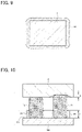
- FIG. 9 is a cross-sectional view of an electronic component body manufactured by performing the blotting process illustrated in FIG. 5A or FIG. 5B ;
- FIG. 10 is a diagram illustrating a coating process that can be performed by the manufacturing apparatus illustrated in FIGS. 3 and 4 ;
- FIG. 11 is a diagram illustrating a coating process according to a comparable example
- FIG. 12 is a diagram illustrating the state of conductive paste at each descent position during the blotting process illustrated in FIG. 5B ;
- FIG. 13 is a diagram illustrating data obtained by evaluating the improved blotting processes and two comparable examples
- FIGS. 14A and 14B are diagrams illustrating a first prepress process that can be performed by the manufacturing apparatus illustrated in FIGS. 3 and 4 ;
- FIGS. 15A and 15B are diagrams illustrating a second prepress process that can be performed by the manufacturing apparatus illustrated in FIGS. 3 and 4 ;
- FIGS. 16A to 16D are diagrams illustrating a coating process that can be performed by the manufacturing apparatus illustrated in FIGS. 3 and 4 .
- first element is described as being “connected” or “coupled” to a second element
- first and second elements are directly connected or coupled to each other
- first and second elements are indirectly connected or coupled to each other with one or more other intervening elements in between.
- first element is described as “moving” relative to the second element
- description includes embodiments in which at least one of the first element and the second element moves relative to the other.
- the present disclosure intends to provide an electronic component manufacturing apparatus that improves processes other than the blotting process to make a conductive paste layer formed at an end portion of an electronic component body uniform in thickness or shape.
- an electronic component manufacturing apparatus d comprising:
- a holding member for holding an electronic component body
- control unit that controls the moving unit to bring an end face of the electronic component body held by the holding member into contact with the surface of the surface plate, and thereafter take the end face of the electronic component body away from the surface of the surface plate
- control unit causing the moving unit to simultaneously perform a distance changing movement for changing a distance between the end face of the electronic component body and the surface of the surface plate and a position changing movement for changing a two-dimensional position where the end face of the electronic component body is projected on the surface of the surface plate in such a manner that the movement direction of the two-dimensional position successively varies in a plane parallel to the surface of the surface plate.
- the position changing movement is simultaneously performed for changing in such a manner that the movement direction of the two-dimensional position of the electronic component body successively varies within the plane parallel to the surface of the surface plate.
- the mounting posture of the electronic component body with respect to the holding member can be corrected, or smooth separation from a dip layer of conductive paste formed on the surface of the surface plate can be realized.
- the conductive paste layer formed at the end portion of the electronic component body can be made uniform in thickness or shape.
- the electronic component manufacturing apparatus wherein the control unit shortens the distance between the end face of the electronic component body and the surface of the surface plate during the distance changing movement, and, at least, at the time of overdrive after bringing the end face of the electronic component body held by the holding member into contact with the surface of the surface plate, can simultaneously perform the distance changing movement and the position changing movement, thereby correcting the posture of the electronic component body held by the holding member.
- the control unit shortens the distance between the end face of the electronic component body and the surface of the surface plate during the distance changing movement, and, at least, at the time of overdrive after bringing the end face of the electronic component body held by the holding member into contact with the surface of the surface plate, can simultaneously perform the distance changing movement and the position changing movement, thereby correcting the posture of the electronic component body held by the holding member.
- the electronic component manufacturing apparatus wherein the holding member can be a jig including an elastic jig body and a hole formed through the jig body and into which the electronic component body is inserted.
- the amount of protrusion (head protrusion amount) by which the electronic component body protrudes from the jig body can be made uniform, and the posture of the electronic component body can be corrected. Further, even when the electronic component body is inclined with respect to the center line of the hole, such an inclination can be eliminated by promoting the insertion of the electronic component body, and the posture of the electronic component body can be corrected.
- the electronic component manufacturing apparatus wherein the holding member can include a base material and an adhesive layer formed on the base material, and the adhesive layer is bonded to a second end face opposite to the end face of the electronic component body.
- the second end face of the electronic component body is entirely directed so as to be bonded to the adhesive layer, and the posture of the electronic component body attached inclinedly to the adhesive layer can be corrected.
- the electronic component manufacturing apparatus wherein the surface of the surface plate is a dip layer of conductive paste
- the control unit simultaneously performs the distance changing movement and the position changing movement after an end portion including the end face of the electronic component body is dipped in the dip layer, and can extend the distance between the end face of the electronic component body and the surface of the surface plate during the distance changing movement.
- the electronic component manufacturing apparatus wherein the holding member can hold a plurality of electronic component bodies including the electronic component body.
- the electronic component manufacturing apparatus wherein in the position changing movement, a movement locus of the two-dimensional position draws a loop, and the distance changing movement and the position changing movement can cause the electronic component body to move spirally with respect to the surface of the surface plate. Accordingly, the position changing process can be efficiently performed while minimizing a required area of the surface plate.
- FIG. 1 illustrates an electronic component 1 A manufactured according to a manufacturing method according to an embodiment of the disclosure.
- FIG. 2 illustrates a cross section of a conductive layer 4 A formed on an electronic component body 1 .
- the electronic component 1 A to which the disclosure is applied is not particularly limited in size, but it is desired that the electronic component 1 A is microminiaturized according to downsizing.
- the microminiaturized electronic component 1 A is rectangular (square or oblong) in cross section.
- L 1 represents the maximum length of one side of the rectangular cross section and L 2 represents the length in a direction orthogonal to the rectangular cross section
- L 1 is 500 ⁇ m or less and L 2 is 1000 ⁇ m or less
- L 1 is 300 ⁇ m or less and L 2 is 600 ⁇ m or less
- L 1 is 200 ⁇ m or less and L 2 is 400 ⁇ m or less
- L 1 is 125 ⁇ m or less and L 2 is 250 ⁇ m or less.
- the term “rectangle” as used herein includes not only the one in which a corner where two sides intersect is strictly 90° but also substantially rectangular shape in which a corner curved or chamfered. It is needless to say that the disclosure can also be applied to any other electronic component 1 A that has a cross section of non-rectangular.
- an electrode 4 A being a conductive paste layer is formed on the electronic component 1 A.
- Each end portion 2 of the electronic component body 1 includes an end face 2 A, an end face 2 B, and a corner portion 2 C connecting the end face 2 A and the end face 2 B.
- thickness T 3 of the electrode 4 A formed on the corner portion 2 C can satisfy a relationship T 3 ⁇ T 1 or T 3 ⁇ T 2 .
- L 3 represents the electrode length of the electrode 4 A formed on the end face 2 B extending from the end face 2 A.
- a plurality of electronic components 1 A when manufactured according to the manufacturing method according to an embodiment of the disclosure, is required to have uniformity in dimensions (T 1 to T 3 and L 3 ) of the electrode 4 A.
- FIG. 3 illustrates a manufacturing apparatus 10 that can be used to implement the present embodiment.
- FIG. 4 is a block diagram illustrating a control system.
- the manufacturing apparatus 10 has a carrier plate (jig) 20 which is holding member for holding the electronic component bodies 1 , a transfer mechanism 50 , and a surface plate 100 .
- X, Y, and Z represent three orthogonal axial directions.
- the carrier plate (jig) 20 which hangs and holds the electronic component bodies 1 , elastically holds the electronic component bodies 1 so as to be movable in a direction perpendicular to a surface 101 of the surface plate 100 .
- the carrier plate 20 can be configured, for example, by an adhesive tape that is elastically deformable in the Z direction.
- the carrier plate 20 is detachably supported by a jig fixing plate 30 .
- a base 40 is fixed above the jig fixing plate 30 , and the surface plate 100 is disposed below the jig fixing plate 30 .
- the surface plate 100 is provided with a squeegee unit 110 including a squeegee 112 and a blade 114 .
- the squeegee unit 110 is movable on the surface plate 100 .
- the blade 114 By moving the blade 114 , the squeegee unit 110 can form a dip layer of a conductive paste 120 having height H on the surface 101 of the surface plate 100 .
- the squeegee unit 110 can scrape the dip layer of the conductive paste 120 from the surface 101 of the surface plate 100 .
- the base 40 is provided with the transfer mechanism 50 for moving the jig fixing plate 30 .
- the transfer mechanism 50 can include an X-axis driving part 60 , a Y-axis driving part 70 , and a Z-axis driving part 80 .
- the transfer mechanism 50 is not particularly limited if it can cause a relative movement between the jig fixing plate 30 and the surface plate 100 in the X-, Y-, and Z-axis directions. That is, the transfer mechanism 50 may be configured to move the surface plate 100 . Alternatively, the transfer mechanism 50 may be configured to include not only the transfer mechanism for moving the jig fixing plate 30 but also another transfer mechanism for moving the surface plate 100 .
- the transfer mechanism 50 may be configured such that at least one of the X-axis driving part 60 , the Y-axis driving part 70 , and the Z-axis driving part 80 causes the jig fixing plate 30 to move and the rest causes the surface plate 100 to move.
- the X-axis driving part 60 can be configured by an X table movable in the X-axis direction with respect to the base 40 along an X-axis guide 62 .
- the Y-axis driving part 70 can be configured by a Y table movable in the Y-axis direction with respect to the X-axis driving part 60 along a Y-axis guide 72 .
- the Z-axis driving part 80 is fixed to, for example, the Y-axis driving part 70 , and can move a Z shaft 82 in the Z-axis direction.
- the jig fixing plate 30 is fixed to the Z shaft 82 .
- FIG. 3 does not include any illustration of X-, Y-, and Z-axis driving sources, such as motors, and driving force transmission mechanisms thereof.
- the transfer mechanism 50 enables the jig fixing plate 30 , the carrier plate 20 , and the electronic component bodies 1 to move relative to the surface plate 100 not only in the Z-axis direction but also along an X-Y plane parallel to the surface of the surface plate 100 .
- the manufacturing apparatus 10 has a controller 90 that controls the X-axis driving part 60 , the Y-axis driving part 70 , and the Z-axis driving part 80 .
- the controller 90 is connected to an operation input unit 92 such as a keyboard or the like.
- the controller 90 includes a storage unit 91 .
- the storage unit 91 stores operational information input via the operation input unit 92 , programs registered in advance, and the like.
- the controller 90 controls the X-axis driving part 60 , the Y-axis driving part 70 , and the Z-axis driving part 80 according to data and programs stored in the storage unit 91 .
- the controller 90 can cause the jig fixing plate 30 to move along, for example, a circular path in a plane parallel to the surface plate 100 (position changing). Further, while the jig fixing plate 30 is moved along the circular path by the X-axis driving part 60 and the Y-axis driving part 70 , the controller 90 can drive the Z-axis driving part 80 to raise or lower the jig fixing plate 30 (distance changing).
- the manufacturing apparatus 10 performs a prepress process, a coating process, and a subsequent blotting process.
- the prepress process is a process of bringing the end face 2 A of each electronic component body 1 of the electronic component bodies 1 held by the carrier plate 20 into contact with the surface plate 100 before the coating process, as described below.
- the coating process is a process of bringing the end portion 2 including the end face 2 A of each of the electronic component bodies 1 held by the carrier plate 20 into contact with the dip layer of conductive paste formed on the surface 101 of the surface plate 100 and coating the conductive paste to the end portion 2 of each of the electronic component bodies 1 .
- the blotting process is a process of bringing the conductive paste coated to each the end portion 2 of the electronic component bodies 1 held by the carrier plate 20 into contact with the surface 101 of the surface plate 100 and transferring a surplus conductive paste to the surface plate 100 .
- FIG. 5A schematically illustrates an improved first blotting process.
- FIG. 5A illustrates an example of relative movement of the surface plate 100 and the electronic component bodies 1 (although only one is illustrated in FIG. 5 ) held by the carrier plate 20 in the blotting process.
- the controller 90 controls the transfer mechanism 50 to cause the carrier plate 20 and the surface plate 100 to move relatively. That is, a projection of the end face 2 A on the surface 101 moves its projected two-dimensional position on the surface 101 .
- FIG. 5A illustrates a spiral motion that is an example of the distance changing process and the position changing process. That is, the controller 90 simultaneously controls the X-axis driving part 60 , the Y-axis driving part 70 , and the Z-axis driving part 80 to raise the electronic component body 1 away from the surface plate 100 while causing the electronic component body 1 to turn in a loop orbit, such as a circle or an ellipse.
- FIG. 5A illustrates positions A to D during ascent of the electronic component body 1 . In FIG. 5A , similar in FIGS.
- the conductive paste layer formed at the end portion 2 of the electronic component body 1 is indicated by reference numeral 4 if the blotting process is not completed yet and by reference numeral 4 A after the completion of the blotting process. Further, the conductive paste transferred to the surface plate 100 is denoted by reference numeral 4 B.
- FIGS. 6A to 6D illustrate blotting operations at respective positions A to D illustrated in FIG. 5A .
- the extra conductive paste 4 B having been brought into contact with the surface plate 100 is transferred to the surface plate 100 while it is dragged toward the downstream side in a horizontal movement direction of the electronic component body 1 , as illustrated in FIGS. 6B and 6C .
- the relative movement direction of the electronic component body 1 with respect to the surface plate 100 successively varies in the plane parallel to the surface plate 100 .
- the conductive paste layer 4 of the electronic component body 1 is dragged by the conductive paste 4 B transferred to the surface plate 100 or the surface plate 100 , the conductive paste layer 4 is easily scraped off since the direction of dragging successively varies.
- the problem such that the extra conductive paste stays downstream in the movement direction does not occur as in the case of linear movement in which the relative movement direction does not successively vary. Therefore, the film thickness of the conductive paste layer 4 A is not locally thickened.
- the extra conductive paste is easily collected at the corner portion 2 C, and it becomes easy to secure the film thickness of the conductive paste at the corner portion 2 C.
- the electronic component body 1 In the distance changing process according to the first blotting process, the electronic component body 1 relatively moves in a direction away from the surface plate 100 during the blotting process. Therefore, the amount of the conductive paste transferred to the surface plate 100 is reduced, and a relatively thick film thickness of the conductive paste of the electronic component body 1 can be secured.
- FIG. 5B schematically illustrates a blotting process according to a second embodiment.
- FIG. 5B is different from FIG. 5A only in that the distance change direction is the downward direction. That is, the controller 90 simultaneously controls the X-axis driving part 60 , the Y-axis driving part 70 , and the Z-axis driving part 80 to lower the electronic component body 1 in such a way as to approach the surface plate 100 while spirally turning.
- FIG. 5B illustrates respective positions A to D during descent of the electronic component body 1 .
- FIGS. 7A to 7D illustrate blotting operations at respective positions A to D illustrated in FIG. 5B .
- the position changing process is performed in the same manner as in the first blotting process.
- the electronic component body 1 relatively moves in a direction approaching the surface plate 100 during the blotting process. Therefore, the amount of the conductive paste transferred to the surface plate 100 is increased, and a relatively thin film thickness of the conductive paste of the electronic component body 1 can be secured.
- implementation of the distance changing process can adjust the amount of the conductive paste to be brought into contact with the surface plate 100 during the blotting process. Therefore, depending on the film thickness of the conductive paste to be secured for the electronic component body 1 , the film thickness can be selectively adjusted by shortening (the first blotting process) or extending (the second blotting process) the distance in the distance changing process.
- This blotting process is such that the extra conductive paste is scraped off during the blotting process including the distance and position changing processes, and the conductive paste does not draw threads after the blotting process. Accordingly, since no trace of threads is left, the surface of the conductive paste layer 4 A of the electronic component body 1 becomes flat.
- the loop locus such as a circular path, an elliptic path, or the like but also starting and end points of the position changing process in the plane parallel to the surface plate 100 do not necessarily coincide if the direction of the relative movement between the electronic component body 1 and the surface plate 100 successively varies in the plane parallel to the surface plate 100 .
- the blotting processes of the first and second blotting processes illustrated in FIGS. 5A and 5B may be implemented in combination.
- the thickness of the conductive paste layer 4 A is different from the thickness of the conductive paste layer 4 A obtained in the blot process of FIG. 5A or FIG. 5B . Accordingly, the freedom degree of the thickness of the conductive paste layer 4 A spreads.
- FIG. 8 illustrates a blotting process in a comparative example, in which extra conductive paste 4 C is transferred to the surface plate 100 by implementing only the position changing process without implementing the distance changing process, while the electronic component body 1 and the surface plate 100 are kept constant in position in the vertical direction.
- the operations illustrated in FIGS. 6 and 7 cannot be performed.
- the blotting process illustrated in FIG. 8 is suitable for leveling the protrusions and shaping the surface of the conductive paste 4 into a flat shape.
- FIG. 9 illustrates a cross-sectional view of the electronic component body 1 obtained by implementing the blotting processes according to the first and second blotting processes.
- the conductive paste layer 4 A formed on the electronic component body 1 has a uniform film thickness on four end faces 2 B continuous from the end face 2 A, and the necessary film thickness of the conductive paste layer 4 A can be secured at the corner portion 2 C.
- a third blotting process uses the blotting process according to the second embodiment to simultaneously perform blotting process on the electronic component bodies 1 .
- FIG. 10 illustrates a coating process.
- a dip layer 121 of the conductive paste 120 ( FIG. 3 ) is formed in advance on the surface 101 of the surface plate 100 .
- the controller 90 controls the transfer mechanism 50 to relatively move the carrier plate 20 and the surface plate 100 in the Z direction, to bring the end face 2 A of each of the electronic component bodies 1 into contact with the surface 101 of the surface plate 100 .
- a right electronic component body 1 a is longer by h than a left electronic component body 1 b .
- the variation h of the length of the electronic component body 1 is, for example, several tens of ⁇ m.
- the movement in the Z direction is continued after the end face 2 A of the electronic component body 1 a on the right side of FIG. 10 is brought into contact with the surface 101 of the surface plate 100 . Therefore, the electronic component body 1 a on the right side of FIG. 10 retracts upward due to elastic deformation of the carrier plate 20 , while maintaining contact with the surface 101 of the surface plate 100 . Then, the relative movement in the Z direction is continued until the end face 2 A of the electronic component body 1 b on the left side of FIG. 10 contacts the surface 101 of the surface plate 100 . At this time, the carrier plate 20 and the surface plate 100 may be relatively moved in the Z direction by an over stroke amount by which the electronic component body 1 b on the left side of FIG.
- FIG. 11 illustrates a coating process in a comparative example.
- a carrier plate 21 illustrated in FIG. 11 does not have a function of holding the electronic component body 1 so as to be elastically movable in the Z direction.
- the relative movement in the Z direction is stopped when the electronic component body 1 a on the right side of FIG. 11 contacts the surface 101 of the surface plate 100 . Therefore, the electronic component body 1 b on the left of FIG. 11 is not in contact with the surface 101 of the surface plate 100 , and the coating length of the electrode 4 A formed on the end portion 2 becomes H 1 ( ⁇ H). Therefore, coating lengths of the electrodes 4 A formed on the end portions 2 between the electronic component bodies 1 become irregular. According to the embodiments of the disclosure, it is possible to prevent the variation in coating length of the electrode 4 A illustrated in FIG. 11 .
- FIG. 12 illustrates the state of two electronic component bodies 1 a and 1 b different in length, during descent, at respective positions A to D illustrated in FIG. 5B , in FIG. 12 , like in FIG. 10 , the right electronic component body 1 a is longer than the left electronic component body 1 b.
- the conductive paste layers 4 of the electronic component bodies 1 a and 1 b do not reach the surface 101 of the surface plate 100 , as illustrated in FIG. 12 .
- the conductive paste layer 4 of the electronic component body 1 a reaches the surface 101 of the surface plate 100 , as illustrated in FIG. 12 .
- the conductive paste layer 4 contacts the surface 101 of the surface plate 100 while changing its position.
- the extra conductive paste is scraped off to the surface plate 100 , and the conductive paste layer 4 remaining on the electronic component body 1 a is shaped while forming threads with the conductive paste transferred to the surface plate 100 .
- the formation of threads by the electronic component body 1 a terminates and the conductive paste layer 4 A is left as a completion form of the blotting process, as illustrated in FIG. 12 .
- the conductive paste layer 4 of the electronic component body 1 b reaches the surface 101 of the surface plate 100 . Subsequently, as the electronic component body 1 b descends spirally, the conductive paste layer 4 contacts the surface 101 of the surface plate 100 while successively changing its position. As a result, the extra conductive paste is scraped off to the surface plate 100 , and the conductive paste layer 4 remaining on the electronic component body 1 b is shaped while forming threads with the conductive paste transferred to the surface plate 100 .
- the formation of threads by the electronic component body 1 b terminates and the conductive paste layer 4 A is left as a completion form of the blotting process, as illustrated in in FIG. 12 .
- the implementation of the blotting process according to the present embodiment can equalize the thicknesses of the conductive paste layers 4 A formed on end faces of the plurality of electronic component bodies 1 a and 1 b even when the plurality of electronic component bodies 1 a and 1 b vary in position of the end face 2 A.
- the conductive paste layers 4 A formed on the end portions 2 of the plurality of electronic component bodies 1 a and 1 b are made uniform in shape. Further, in this blotting process, the height changing process and the position changing process are simultaneously performed.
- the plurality of electronic component bodies 1 a and 1 b relatively move closer to the surface plate 100 , the plurality of electronic component bodies 1 a and 1 b are relatively moved with the component in a direction parallel to the surface plate 100 . Further, causing the plurality of electronic component bodies 1 a and 1 b to move relatively and spirally so as to approach the surface 101 of the surface plate 100 can efficiently implement the position changing process while minimizing the required area of the surface plate 100 .
- the coating process illustrated in FIG. 10 and the blotting process illustrated in FIGS. 5B and 12 may be implemented.
- the length L 3 ( FIG. 2 ) of the coating formed on the end portion 2 of each of the plurality of electronic component bodies 1 a and 1 b coincides with the height H of the dip layer 121 .
- the thicknesses T 1 ( FIG. 2 ) of the conductive paste layers 4 A formed on the end faces of the plurality of electronic component bodies 1 a and 1 b are made uniform. This is because the electrode 4 A formed on the end portion 2 of each of the electronic component bodies 1 is independently made uniform in shape.
- FIG. 13 illustrates representative evaluation data obtained by implementing the blotting processes in comparative examples 1 and 2 and the present embodiment for the electronic component bodies 1 a and 1 b different in length.
- the comparative example 1 uses the blotting process disclosed in JP-A-63-45813
- the comparative example 2 uses the blotting process in which the electronic component body 1 is moved linearly with respect to the surface plate 100 .
- the difference of the conductive paste layer 4 a in TOP film thickness (film thickness T 1 in FIG. 2 ) occurring due to the difference in length between the electronic component bodies 1 a and 1 b was as large as 7 to 8 ⁇ m.
- the difference in TOP film thickness of the conductive paste layer 4 a was reduced to 2 ⁇ m. From this, the uniformization effect of the thickness T 1 ( FIG. 2 ) of the conductive paste layer 4 A by the blotting process illustrated in FIGS. 5 and 12 is understood.
- the blotting process illustrated in FIGS. 5B and 12 may not necessarily use the carrier plate 20 used in the coating process illustrated in FIG. 10 , because the blotting process does not require the elastic deformation of the carrier plate 20 . Further, in the coating process illustrated in FIG. 10 and in the blotting process illustrated in FIGS. 5B and 12 , it is unnecessary to use the same surface plate 100 .
- a first surface plate may be used in the coating process illustrated in FIG. 10
- a second surface plate may be used in the blotting process illustrated in FIGS. 5B and 12 .
- FIGS. 14A and 14B illustrate a first prepress process.
- the jig 20 holding the electronic component body 1 has a hole 22 formed in a jig body 21 made of an elastic body, such as silicon rubber.
- the electronic component body 1 is inserted and held in the hole 22 .
- the prepress process is performed, using the manufacturing apparatus 10 illustrated in FIGS. 3 and 4 , by relatively moving the jig 20 holding the electronic component body 1 inserted in the hole 22 of the jig body 21 and the surface plate 100 , in the prepress process, the end face 2 A of the electronic component body 1 is brought into contact with the surface 101 of the surface plate 100 .
- the amount of protrusion (head protrusion amount) of the electronic component body 1 protruding from the jig 20 that is the position of protrusion (head protrusion position) of the end face 2 A of the electronic component body 1 , can be corrected so as to be constant.
- the posture including the insertion length or orientation of the electronic component body 1 with respect to the hole 22 of the jig body 21 varies. This is because, at the time of insertion of the electronic component body 1 , the posture of the electronic component body 1 varies with respect to the hole 22 , and the elastic jig body 21 is deformed.
- the jig 20 is linearly moved downward with respect to the surface plate 100 .
- the electronic component body 1 will be pushed back at the time of overdrive after the end face 2 A of the electronic component body 1 is brought into contact with the surface 101 of the surface plate 100 .
- the amount of protrusion (head protrusion amount) of the electronic component body 1 can be made uniform.
- the jig body 21 pushed by the electronic component body 1 may be elastically deformed.
- an adverse effect may arise in such a manner that only the jig body 21 is elastically restored and the amount of protrusion (head protrusion amount) of the electronic component body 1 is not changed.
- a distance shortening movement and a position changing movement are simultaneously performed in the same manner as in FIG. 5B .
- the conductive paste layer 4 is not formed on the electronic component body 1 as illustrated in FIG. 14B .
- simultaneously performing the distance shortening movement and the position changing movement at least during the overdrive will be satisfactory, but the simultaneous execution of these movements may be performed before the overdrive.
- the external force whose orientation varies successively within the plane parallel to the surface 101 of the surface plate 100 acts on the electronic component body 1 . Therefore, even when the jig body 21 is elastically deformed, the insertion of the electronic component body 1 into the hole 22 of the jig body 21 is promoted. Thus, the amount of protrusion (head protrusion amount) of the electronic component body 1 can be made uniform, and the posture of the electronic component body 1 can be corrected.
- head protrusion amount head protrusion amount of the electronic component body 1 can be made uniform, and the posture of the electronic component body 1 can be corrected.
- FIG. 14A even when the electronic component body 1 is inclined with respect to the center line of the hole 22 , such an inclination can be eliminated by promoting the insertion of the electronic component body 1 , and the posture of the electronic component body 1 can be corrected.
- FIGS. 15A and 15B illustrate a second prepress process.
- the holding member 23 for holding the electronic component body 1 includes an adhesive layer 25 on one surface of a base material 24 .
- the base material 24 may be a rigid body or a flexible member such as a tape.
- one end face 2 A is bonded to the adhesive layer 25 , and a conductive paste is applied to an end portion including the other end face 2 A.
- the posture including the orientation of the electronic component body 1 with respect to the hole 22 of the jig body 21 varies as illustrated in FIG. 15A .
- This variation in posture cannot be corrected by only linearly moving the holding member 23 downward with respect to the surface plate 100 , like the conventional prepress process. This is because the inclined posture of the electronic component body 1 may be maintained while only a corner of the end face 2 A of the inclined electronic component body 1 is in contact with the surface plate 100 .
- the distance shortening movement and the position changing movement are simultaneously performed. Even in FIG. 15B , like FIG. 14B , simultaneously performing the distance shortening movement and the position changing movement at least during the overdrive will be satisfactory, but the simultaneous execution of these movements may be performed before the overdrive.
- the external force whose orientation varies successively within the plane parallel to the surface 101 of the surface plate 100 acts on the electronic component body 1 . Therefore, even when only a corner of the end face 2 A of the inclined electronic component body 1 is in contact with the surface plate 100 , the end face 2 A of the electronic component body 1 is entirely directed so as to be bonded to the adhesive layer 25 by the successively changing external force. Thus, the posture of the electronic component body 1 can be corrected.
- the base material 24 is a flexible member, a rigid body is disposed on the back surface of the base material 24 during the relative movement of the holding member 23 , and the base material 24 can be prevented from being deformed.
- the improved prepress process is performed before the coating process described below, and the prepress process and the coating process can be performed by using the manufacturing apparatus 10 illustrated in FIGS. 3 and 4 .
- the above-described blotting process comparativable example 1, comparable example 2, or improved blotting process
- the blotting process itself may be omitted. This is because the thickness or shape of the conductive paste layer formed on the end portion 2 of the electronic component body 1 can be made uniform by the improved coating process.
- the surface of the surface plate 100 is the dip layer 121 of conductive paste.
- a relative movement illustrated in FIGS. 16A to 16D is performed.
- FIGS. 16A to 16D a distance extending movement and a position changing movement are simultaneously performed in the same manner as in FIG. 5A .
- FIG. 16A illustrates an initial state where the electronic component body 1 is separated from the surface plate 100 .
- the conductive paste layer 4 formed at the end portion of the electronic component body 1 is completely separated from the dip layer 121 as illustrated in FIG. 16D .
- the relative movement illustrated in FIGS. 16A to 16D functions like the improved blotting process illustrated in FIGS. 6A to 6D . In other words, by performing the movement process illustrated in FIGS.
- the separation process becomes similar to the improved blotting process illustrated in FIGS. 6A to 6D . As a result, it becomes possible to omit the blotting process after the improved coating process.
Landscapes
- Engineering & Computer Science (AREA)
- Power Engineering (AREA)
- Microelectronics & Electronic Packaging (AREA)
- Manufacturing & Machinery (AREA)
- Chemical & Material Sciences (AREA)
- Physics & Mathematics (AREA)
- Electromagnetism (AREA)
- Inorganic Chemistry (AREA)
- Ceramic Engineering (AREA)
- Fixed Capacitors And Capacitor Manufacturing Machines (AREA)
- Coating Apparatus (AREA)
- Application Of Or Painting With Fluid Materials (AREA)
- Ceramic Capacitors (AREA)
- Apparatuses And Processes For Manufacturing Resistors (AREA)
- Coils Or Transformers For Communication (AREA)
- Manufacturing Cores, Coils, And Magnets (AREA)
Abstract
Description
Claims (20)
Applications Claiming Priority (7)
| Application Number | Priority Date | Filing Date | Title |
|---|---|---|---|
| JP2018130961 | 2018-07-10 | ||
| JP2018-130961 | 2018-07-10 | ||
| JPJP2018-130961 | 2018-07-10 | ||
| JP2018-168952 | 2018-09-10 | ||
| JPJP2018-168952 | 2018-09-10 | ||
| JP2018168952 | 2018-09-10 | ||
| PCT/JP2019/027369 WO2020013237A1 (en) | 2018-07-10 | 2019-07-10 | Electronic component manufacturing device |
Related Parent Applications (1)
| Application Number | Title | Priority Date | Filing Date |
|---|---|---|---|
| PCT/JP2019/027369 Continuation WO2020013237A1 (en) | 2018-07-10 | 2019-07-10 | Electronic component manufacturing device |
Publications (2)
| Publication Number | Publication Date |
|---|---|
| US20200147639A1 US20200147639A1 (en) | 2020-05-14 |
| US11338317B2 true US11338317B2 (en) | 2022-05-24 |
Family
ID=67437534
Family Applications (3)
| Application Number | Title | Priority Date | Filing Date |
|---|---|---|---|
| US16/503,288 Active 2039-08-28 US11052422B2 (en) | 2018-07-10 | 2019-07-03 | Electronic component manufacturing method and apparatus |
| US16/738,374 Expired - Fee Related US11338317B2 (en) | 2018-07-10 | 2020-01-09 | Electronic component manufacturing apparatus |
| US17/348,682 Active 2039-08-23 US11602766B2 (en) | 2018-07-10 | 2021-06-15 | Electronic component manufacturing method and apparatus |
Family Applications Before (1)
| Application Number | Title | Priority Date | Filing Date |
|---|---|---|---|
| US16/503,288 Active 2039-08-28 US11052422B2 (en) | 2018-07-10 | 2019-07-03 | Electronic component manufacturing method and apparatus |
Family Applications After (1)
| Application Number | Title | Priority Date | Filing Date |
|---|---|---|---|
| US17/348,682 Active 2039-08-23 US11602766B2 (en) | 2018-07-10 | 2021-06-15 | Electronic component manufacturing method and apparatus |
Country Status (7)
| Country | Link |
|---|---|
| US (3) | US11052422B2 (en) |
| EP (1) | EP3598467B1 (en) |
| JP (2) | JP6787605B2 (en) |
| KR (2) | KR102587410B1 (en) |
| CN (2) | CN110706924B (en) |
| TW (2) | TWI749337B (en) |
| WO (1) | WO2020013237A1 (en) |
Families Citing this family (9)
| Publication number | Priority date | Publication date | Assignee | Title |
|---|---|---|---|---|
| US11052422B2 (en) | 2018-07-10 | 2021-07-06 | Creative Coatings Co., Ltd. | Electronic component manufacturing method and apparatus |
| EP4120299A4 (en) * | 2020-03-11 | 2023-07-19 | Creative Coatings Co., Ltd. | METHOD AND DEVICE FOR MANUFACTURING ELECTRONIC COMPONENTS |
| JP7079511B2 (en) * | 2020-04-02 | 2022-06-02 | 株式会社クリエイティブコーティングス | Manufacturing method of electronic parts |
| JP7283821B2 (en) * | 2020-04-02 | 2023-05-30 | 株式会社クリエイティブコーティングス | Electronic component manufacturing equipment |
| WO2022075135A1 (en) | 2020-10-05 | 2022-04-14 | 株式会社クリエイティブコーティングス | Positioning jig assembly, positioning jig, positioning method for electronic component body, and method for mounting same to transport jig |
| JP2022098614A (en) * | 2020-12-22 | 2022-07-04 | 株式会社村田製作所 | Manufacturing device of electronic component and manufacturing method of electronic component |
| JP7398122B2 (en) * | 2021-06-03 | 2023-12-14 | 株式会社クリエイティブコーティングス | Electronic component manufacturing method and paste coating device |
| WO2024038690A1 (en) * | 2022-08-19 | 2024-02-22 | 株式会社クリエイティブコーティングス | Method and device for transferring electronic component |
| CN115990567A (en) * | 2022-12-30 | 2023-04-21 | 东莞顺络电子有限公司 | An inductive magnetic glue coating device and method |
Citations (9)
| Publication number | Priority date | Publication date | Assignee | Title |
|---|---|---|---|---|
| JPS6345813A (en) | 1986-08-13 | 1988-02-26 | 株式会社村田製作所 | Method of forming electrode of electronic parts |
| JPH04291712A (en) | 1991-03-20 | 1992-10-15 | Murata Mfg Co Ltd | Holder for electronic part chip and method of operating electronic part chip |
| JPH05182879A (en) | 1991-12-31 | 1993-07-23 | Taiyo Yuden Co Ltd | Small part edge coating method and device |
| JP2002237403A (en) | 2001-02-07 | 2002-08-23 | Atc Protech Kk | Method and apparatus for attaching electrodes to electronic component body |
| US7673382B2 (en) * | 2006-01-16 | 2010-03-09 | Tdk Corporation | External electrode forming method |
| US20120128865A1 (en) * | 2010-11-22 | 2012-05-24 | Samsung Electro-Mechanics Co., Ltd. | Apparatus for forming electrode and method for forming electrode using the same |
| JP2016100459A (en) | 2014-11-21 | 2016-05-30 | 株式会社クリエゾン | Electronic component manufacturing method and apparatus, and electronic component |
| WO2018070093A1 (en) | 2016-10-14 | 2018-04-19 | 株式会社クリエゾン | Method and apparatus for manufacturing electronic component, and electronic component |
| US20200016624A1 (en) | 2018-07-10 | 2020-01-16 | Creative Coatings Co., Ltd. | Electronic component manufacturing method and apparatus |
Family Cites Families (20)
| Publication number | Priority date | Publication date | Assignee | Title |
|---|---|---|---|---|
| JPS5987073A (en) * | 1982-11-10 | 1984-05-19 | Canon Inc | Application method |
| JPH0636899B2 (en) * | 1990-03-17 | 1994-05-18 | 太陽誘電株式会社 | How to apply paste to the edges of electronic components |
| JP2934029B2 (en) * | 1991-02-18 | 1999-08-16 | 太陽誘電株式会社 | How to attach conductive paste for external electrode |
| US5254362A (en) * | 1992-10-23 | 1993-10-19 | Motorola, Inc. | Method and apparatus for deposition of solder paste on a printed wiring board |
| JP3641217B2 (en) * | 2000-03-31 | 2005-04-20 | Tdk株式会社 | End electrode forming method and apparatus for chip-shaped electronic component |
| US7038142B2 (en) * | 2002-01-24 | 2006-05-02 | Fujitsu Limited | Circuit board and method for fabricating the same, and electronic device |
| JP2004273367A (en) * | 2003-03-11 | 2004-09-30 | Seiko Epson Corp | Method for manufacturing conductive pattern, electro-optical device, and electronic apparatus |
| JP2005203396A (en) * | 2004-01-13 | 2005-07-28 | Toshiba Corp | Electronic component manufacturing apparatus, electronic component manufacturing method, and electronic component |
| CN101213627B (en) * | 2005-07-08 | 2012-05-09 | 株式会社村田制作所 | Method and apparatus for forming outer electrode of electronic component |
| JP2009090479A (en) * | 2007-10-04 | 2009-04-30 | Panasonic Corp | Pad printing apparatus, coating layer forming method, and optical component |
| JP4561826B2 (en) * | 2007-12-28 | 2010-10-13 | Tdk株式会社 | Manufacturing method of multilayer electronic component |
| CN101408525B (en) * | 2008-09-09 | 2010-06-23 | 深圳市日理江澍实业有限公司 | Method for preparing oxygen sensor external platinum electrode |
| JP4636196B2 (en) * | 2009-05-27 | 2011-02-23 | 株式会社村田製作所 | Component alignment apparatus and electronic component manufacturing method |
| JP2012028465A (en) * | 2010-07-21 | 2012-02-09 | Tdk Corp | Electronic component manufacturing method |
| JP6386266B2 (en) * | 2014-06-27 | 2018-09-05 | テイ・エス テック株式会社 | Storage container |
| JP2016082209A (en) * | 2014-10-22 | 2016-05-16 | 株式会社村田製作所 | Device and method for chip manufacturing |
| JP2016137437A (en) * | 2015-01-27 | 2016-08-04 | 株式会社デンソー | Coating apparatus and coating method |
| CN108074691A (en) * | 2016-11-11 | 2018-05-25 | 株式会社创力艾生 | The manufacturing method and apparatus and electronic unit of electronic unit |
| EP3363562A1 (en) | 2017-02-16 | 2018-08-22 | Siemens Aktiengesellschaft | Improved additive manufacturing |
| JP2018168952A (en) | 2017-03-30 | 2018-11-01 | Ntn株式会社 | Grease supplying bearing spacer/bearing assembly and spindle device |
-
2019
- 2019-07-03 US US16/503,288 patent/US11052422B2/en active Active
- 2019-07-04 JP JP2019125369A patent/JP6787605B2/en active Active
- 2019-07-04 EP EP19184381.2A patent/EP3598467B1/en active Active
- 2019-07-08 CN CN201910609337.5A patent/CN110706924B/en active Active
- 2019-07-09 TW TW108122767A patent/TWI749337B/en active
- 2019-07-10 WO PCT/JP2019/027369 patent/WO2020013237A1/en not_active Ceased
- 2019-07-10 JP JP2020524263A patent/JP6787620B2/en active Active
- 2019-07-10 CN CN201980006818.5A patent/CN111512402B/en active Active
- 2019-07-10 KR KR1020190083207A patent/KR102587410B1/en active Active
- 2019-07-10 KR KR1020207012795A patent/KR102809609B1/en active Active
- 2019-07-10 TW TW108124220A patent/TWI720537B/en active
-
2020
- 2020-01-09 US US16/738,374 patent/US11338317B2/en not_active Expired - Fee Related
-
2021
- 2021-06-15 US US17/348,682 patent/US11602766B2/en active Active
Patent Citations (10)
| Publication number | Priority date | Publication date | Assignee | Title |
|---|---|---|---|---|
| JPS6345813A (en) | 1986-08-13 | 1988-02-26 | 株式会社村田製作所 | Method of forming electrode of electronic parts |
| JPH04291712A (en) | 1991-03-20 | 1992-10-15 | Murata Mfg Co Ltd | Holder for electronic part chip and method of operating electronic part chip |
| US5383997A (en) | 1991-03-20 | 1995-01-24 | Murata Manufacturing Co., Ltd. | Method of handling electronic component chips |
| JPH05182879A (en) | 1991-12-31 | 1993-07-23 | Taiyo Yuden Co Ltd | Small part edge coating method and device |
| JP2002237403A (en) | 2001-02-07 | 2002-08-23 | Atc Protech Kk | Method and apparatus for attaching electrodes to electronic component body |
| US7673382B2 (en) * | 2006-01-16 | 2010-03-09 | Tdk Corporation | External electrode forming method |
| US20120128865A1 (en) * | 2010-11-22 | 2012-05-24 | Samsung Electro-Mechanics Co., Ltd. | Apparatus for forming electrode and method for forming electrode using the same |
| JP2016100459A (en) | 2014-11-21 | 2016-05-30 | 株式会社クリエゾン | Electronic component manufacturing method and apparatus, and electronic component |
| WO2018070093A1 (en) | 2016-10-14 | 2018-04-19 | 株式会社クリエゾン | Method and apparatus for manufacturing electronic component, and electronic component |
| US20200016624A1 (en) | 2018-07-10 | 2020-01-16 | Creative Coatings Co., Ltd. | Electronic component manufacturing method and apparatus |
Also Published As
| Publication number | Publication date |
|---|---|
| JP6787620B2 (en) | 2020-11-18 |
| JPWO2020013237A1 (en) | 2020-08-20 |
| KR102587410B1 (en) | 2023-10-11 |
| US20210308717A1 (en) | 2021-10-07 |
| US11052422B2 (en) | 2021-07-06 |
| TW202016957A (en) | 2020-05-01 |
| TW202006756A (en) | 2020-02-01 |
| CN110706924B (en) | 2022-04-01 |
| EP3598467B1 (en) | 2022-08-31 |
| CN110706924A (en) | 2020-01-17 |
| CN111512402A (en) | 2020-08-07 |
| JP6787605B2 (en) | 2020-11-18 |
| KR20200006505A (en) | 2020-01-20 |
| US11602766B2 (en) | 2023-03-14 |
| US20200016624A1 (en) | 2020-01-16 |
| KR102809609B1 (en) | 2025-05-21 |
| JP2020043330A (en) | 2020-03-19 |
| CN111512402B (en) | 2023-02-21 |
| US20200147639A1 (en) | 2020-05-14 |
| TWI749337B (en) | 2021-12-11 |
| TWI720537B (en) | 2021-03-01 |
| EP3598467A1 (en) | 2020-01-22 |
| WO2020013237A1 (en) | 2020-01-16 |
| KR20210030893A (en) | 2021-03-18 |
Similar Documents
| Publication | Publication Date | Title |
|---|---|---|
| US20200147639A1 (en) | Electronic component manufacturing apparatus | |
| EP3716741B1 (en) | Three-dimensional multi-layer electronic device production method and three-dimensional multi-layer electronic device | |
| TW201813724A (en) | Manufacturing method and device of electric components and electric components capable of making coating thickness of conductive paste layer uniform | |
| US12565006B2 (en) | Production method and production device for three-dimensionally fabricated object | |
| US9421665B2 (en) | Pressure-adjusting lapping element | |
| CN112286235B (en) | Trajectory-based control method | |
| JP2021057448A (en) | Manufacturing apparatus and manufacturing method of electronic component | |
| JP7224000B2 (en) | LIQUID MATERIAL SUPPLY DEVICE AND LIQUID MATERIAL SUPPLY METHOD | |
| CN108074691A (en) | The manufacturing method and apparatus and electronic unit of electronic unit | |
| CN102049364A (en) | Coating device and coating method | |
| EP4120299A1 (en) | Electronic component manufacturing method and device | |
| JP6242122B2 (en) | Coating unit, coating apparatus and coating method using the same | |
| JP2014116393A (en) | Substrate support device and method, and mounting device and method | |
| US12048102B2 (en) | Electronic circuit production method using 3D layer shaping | |
| JP7199507B2 (en) | Deposition equipment and mounter | |
| KR20250044349A (en) | Method and device for transferring electronic components | |
| JPH1041617A (en) | Viscous material supply device and viscous material application method | |
| JP2008193114A (en) | Component mounting method |
Legal Events
| Date | Code | Title | Description |
|---|---|---|---|
| FEPP | Fee payment procedure |
Free format text: ENTITY STATUS SET TO UNDISCOUNTED (ORIGINAL EVENT CODE: BIG.); ENTITY STATUS OF PATENT OWNER: SMALL ENTITY |
|
| FEPP | Fee payment procedure |
Free format text: ENTITY STATUS SET TO SMALL (ORIGINAL EVENT CODE: SMAL); ENTITY STATUS OF PATENT OWNER: SMALL ENTITY |
|
| STPP | Information on status: patent application and granting procedure in general |
Free format text: DOCKETED NEW CASE - READY FOR EXAMINATION |
|
| STPP | Information on status: patent application and granting procedure in general |
Free format text: NON FINAL ACTION MAILED |
|
| STPP | Information on status: patent application and granting procedure in general |
Free format text: RESPONSE TO NON-FINAL OFFICE ACTION ENTERED AND FORWARDED TO EXAMINER |
|
| STPP | Information on status: patent application and granting procedure in general |
Free format text: NON FINAL ACTION MAILED |
|
| STPP | Information on status: patent application and granting procedure in general |
Free format text: RESPONSE TO NON-FINAL OFFICE ACTION ENTERED AND FORWARDED TO EXAMINER |
|
| STPP | Information on status: patent application and granting procedure in general |
Free format text: NOTICE OF ALLOWANCE MAILED -- APPLICATION RECEIVED IN OFFICE OF PUBLICATIONS |
|
| STPP | Information on status: patent application and granting procedure in general |
Free format text: PUBLICATIONS -- ISSUE FEE PAYMENT VERIFIED |
|
| STCF | Information on status: patent grant |
Free format text: PATENTED CASE |
|
| FEPP | Fee payment procedure |
Free format text: MAINTENANCE FEE REMINDER MAILED (ORIGINAL EVENT CODE: REM.); ENTITY STATUS OF PATENT OWNER: SMALL ENTITY |
|
| LAPS | Lapse for failure to pay maintenance fees |
Free format text: PATENT EXPIRED FOR FAILURE TO PAY MAINTENANCE FEES (ORIGINAL EVENT CODE: EXP.); ENTITY STATUS OF PATENT OWNER: SMALL ENTITY |
|
| STCH | Information on status: patent discontinuation |
Free format text: PATENT EXPIRED DUE TO NONPAYMENT OF MAINTENANCE FEES UNDER 37 CFR 1.362 |
|
| FP | Lapsed due to failure to pay maintenance fee |
Effective date: 20260524 |