US11367720B2 - Method for protecting an integrated circuit module using an antifuse, and corresponding device - Google Patents
Method for protecting an integrated circuit module using an antifuse, and corresponding device Download PDFInfo
- Publication number
- US11367720B2 US11367720B2 US16/518,436 US201916518436A US11367720B2 US 11367720 B2 US11367720 B2 US 11367720B2 US 201916518436 A US201916518436 A US 201916518436A US 11367720 B2 US11367720 B2 US 11367720B2
- Authority
- US
- United States
- Prior art keywords
- electrically conductive
- integrated circuit
- terminal
- circuit
- conductive body
- Prior art date
- Legal status (The legal status is an assumption and is not a legal conclusion. Google has not performed a legal analysis and makes no representation as to the accuracy of the status listed.)
- Active, expires
Links
Images


Classifications
-
- H01L27/0292—
-
- G—PHYSICS
- G06—COMPUTING OR CALCULATING; COUNTING
- G06K—GRAPHICAL DATA READING; PRESENTATION OF DATA; RECORD CARRIERS; HANDLING RECORD CARRIERS
- G06K19/00—Record carriers for use with machines and with at least a part designed to carry digital markings
- G06K19/06—Record carriers for use with machines and with at least a part designed to carry digital markings characterised by the kind of the digital marking, e.g. shape, nature, code
- G06K19/067—Record carriers with conductive marks, printed circuits or semiconductor circuit elements, e.g. credit or identity cards also with resonating or responding marks without active components
- G06K19/07—Record carriers with conductive marks, printed circuits or semiconductor circuit elements, e.g. credit or identity cards also with resonating or responding marks without active components with integrated circuit chips
- G06K19/073—Special arrangements for circuits, e.g. for protecting identification code in memory
- G06K19/07309—Means for preventing undesired reading or writing from or onto record carriers
-
- H—ELECTRICITY
- H10—SEMICONDUCTOR DEVICES; ELECTRIC SOLID-STATE DEVICES NOT OTHERWISE PROVIDED FOR
- H10D—INORGANIC ELECTRIC SEMICONDUCTOR DEVICES
- H10D89/00—Aspects of integrated devices not covered by groups H10D84/00 - H10D88/00
- H10D89/60—Integrated devices comprising arrangements for electrical or thermal protection, e.g. protection circuits against electrostatic discharge [ESD]
- H10D89/601—Integrated devices comprising arrangements for electrical or thermal protection, e.g. protection circuits against electrostatic discharge [ESD] for devices having insulated gate electrodes, e.g. for IGFETs or IGBTs
- H10D89/921—Integrated devices comprising arrangements for electrical or thermal protection, e.g. protection circuits against electrostatic discharge [ESD] for devices having insulated gate electrodes, e.g. for IGFETs or IGBTs characterised by the configuration of the interconnections connecting the protective arrangements, e.g. ESD buses
-
- G—PHYSICS
- G06—COMPUTING OR CALCULATING; COUNTING
- G06K—GRAPHICAL DATA READING; PRESENTATION OF DATA; RECORD CARRIERS; HANDLING RECORD CARRIERS
- G06K19/00—Record carriers for use with machines and with at least a part designed to carry digital markings
- G06K19/06—Record carriers for use with machines and with at least a part designed to carry digital markings characterised by the kind of the digital marking, e.g. shape, nature, code
- G06K19/067—Record carriers with conductive marks, printed circuits or semiconductor circuit elements, e.g. credit or identity cards also with resonating or responding marks without active components
- G06K19/07—Record carriers with conductive marks, printed circuits or semiconductor circuit elements, e.g. credit or identity cards also with resonating or responding marks without active components with integrated circuit chips
- G06K19/073—Special arrangements for circuits, e.g. for protecting identification code in memory
- G06K19/07309—Means for preventing undesired reading or writing from or onto record carriers
- G06K19/07372—Means for preventing undesired reading or writing from or onto record carriers by detecting tampering with the circuit
- G06K19/07381—Means for preventing undesired reading or writing from or onto record carriers by detecting tampering with the circuit with deactivation or otherwise incapacitation of at least a part of the circuit upon detected tampering
-
- H01L23/5252—
-
- H—ELECTRICITY
- H10—SEMICONDUCTOR DEVICES; ELECTRIC SOLID-STATE DEVICES NOT OTHERWISE PROVIDED FOR
- H10W—GENERIC PACKAGES, INTERCONNECTIONS, CONNECTORS OR OTHER CONSTRUCTIONAL DETAILS OF DEVICES COVERED BY CLASS H10
- H10W20/00—Interconnections in chips, wafers or substrates
- H10W20/40—Interconnections external to wafers or substrates, e.g. back-end-of-line [BEOL] metallisations or vias connecting to gate electrodes
- H10W20/49—Adaptable interconnections, e.g. fuses or antifuses
- H10W20/491—Antifuses, i.e. interconnections changeable from non-conductive to conductive
-
- H—ELECTRICITY
- H10—SEMICONDUCTOR DEVICES; ELECTRIC SOLID-STATE DEVICES NOT OTHERWISE PROVIDED FOR
- H10W—GENERIC PACKAGES, INTERCONNECTIONS, CONNECTORS OR OTHER CONSTRUCTIONAL DETAILS OF DEVICES COVERED BY CLASS H10
- H10W42/00—Arrangements for protection of devices
-
- H—ELECTRICITY
- H10—SEMICONDUCTOR DEVICES; ELECTRIC SOLID-STATE DEVICES NOT OTHERWISE PROVIDED FOR
- H10W—GENERIC PACKAGES, INTERCONNECTIONS, CONNECTORS OR OTHER CONSTRUCTIONAL DETAILS OF DEVICES COVERED BY CLASS H10
- H10W42/00—Arrangements for protection of devices
- H10W42/40—Arrangements for protection of devices protecting against tampering, e.g. unauthorised inspection or reverse engineering
- H10W42/405—Arrangements for protection of devices protecting against tampering, e.g. unauthorised inspection or reverse engineering using active circuits
-
- G—PHYSICS
- G11—INFORMATION STORAGE
- G11C—STATIC STORES
- G11C17/00—Read-only memories programmable only once; Semi-permanent stores, e.g. manually-replaceable information cards
- G11C17/14—Read-only memories programmable only once; Semi-permanent stores, e.g. manually-replaceable information cards in which contents are determined by selectively establishing, breaking or modifying connecting links by permanently altering the state of coupling elements, e.g. PROM
- G11C17/18—Auxiliary circuits, e.g. for writing into memory
-
- H—ELECTRICITY
- H10—SEMICONDUCTOR DEVICES; ELECTRIC SOLID-STATE DEVICES NOT OTHERWISE PROVIDED FOR
- H10W—GENERIC PACKAGES, INTERCONNECTIONS, CONNECTORS OR OTHER CONSTRUCTIONAL DETAILS OF DEVICES COVERED BY CLASS H10
- H10W42/00—Arrangements for protection of devices
- H10W42/40—Arrangements for protection of devices protecting against tampering, e.g. unauthorised inspection or reverse engineering
Definitions
- Embodiments and implementations relate to integrated circuits, in particular to the protection thereof, more particularly during a potential attempt to breach the integrity of the integrated circuit, for example through an attack carried out by means of a focused ion beam (FIB) of positively charged particles or through negatively charged particles, such as electrons in the context of scanning electron microscopy (SEM).
- FIB focused ion beam
- SEM scanning electron microscopy
- Integrated circuits in particular those provided with memories containing sensitive information, have to be protected to the greatest possible extent from attacks, in particular from attacks aiming to uncover stored data.
- a method for protecting a module within an integrated circuit comprising: producing, in the integrated circuit, an electrically conductive body at a floating potential and holding an initial amount of electric charge; and grounding an output of the module in the presence of an amount of electric charge on said body that is different from said initial amount and higher than a threshold.
- module should be understood very broadly, including in particular a memory, and more generally a data storage circuit, or else an electronic circuit having a determined function in the integrated circuit, for example, but not exclusively, an amplifier or filter function.
- An electrically conductive body at a floating potential makes it possible to collect electric charge during an attack, for example by ion or electron beams. If the amount of electric charge is higher than the threshold, said output of the module will be grounded. Thus, it will not be possible to retrieve the information processed or stored by the module and the module is protected.
- the threshold depends in particular on the circuit used to ground the output of the module. Thus, if an antifuse device is used, a threshold value corresponding to a breakdown voltage of the antifuse device could be chosen.
- This threshold will generally allow the circuit allowing the output of the module to be grounded to be activated or triggered.
- a person skilled in the art will be able to choose the value of the threshold according to the structure and the operation of said circuit, in particular its trigger threshold.
- the initial charge state may take any value, it is simpler for the initial charge amount to be zero.
- the production of the body at a floating potential comprises grounding said body via a connecting element during the production of the integrated circuit then cutting through the connecting element so as to confer a zero initial amount of charge on said body.
- the body at a floating potential is thus grounded during the production of the integrated circuit in order to shed charge and to provide it with a discharged initial state before any potential attack.
- the method comprises an electrically conductive coupling from a terminal of an antifuse device to said body, said antifuse device being configured to transition irreversibly from a first state corresponding to an open circuit to a second state corresponding to a closed circuit if the voltage applied to said terminal and resulting from said amount of charge that is higher than said threshold is higher than a breakdown voltage of said antifuse device, the transitioning of the antifuse device from the first state to the second state then comprises the formation, within the antifuse device, of a permanent electrically conductive path connecting said output of said module to ground.
- the antifuse device changes state.
- the device that is coupled to ground but configured in an initial off state then becomes conductive, thus allowing the data present at the output of the module to be transmitted to ground and thus the module to be protected.
- an integrated circuit comprising a module, an electrically conductive body at a floating potential that is located in the integrated circuit and holds an initial amount of electric charge, and a protection circuit that is configured to ground an output of the module in the presence of an amount of electric charge on said body that is different from the initial amount and higher than a threshold.
- the body is configured to hold a zero initial amount of charge.
- the integrated circuit comprises an electrically conductive connecting element having a first end that is coupled to said body and a second, free end that is located outside the integrated circuit.
- the integrated circuit comprises at least one sealing ring, and said connecting element passes through said at least one sealing ring, the free end of the connecting element being located outside said at least one sealing ring.
- the protection circuit comprises an antifuse device having a terminal that is electrically coupled to said body, said antifuse device being configured to transition irreversibly from a first state corresponding to an open circuit to a second state corresponding to a closed circuit if the voltage applied to said terminal and resulting from said amount of charge that is higher than said threshold is higher than a breakdown voltage of said antifuse device, the antifuse device being configured to form a permanent electrically conductive path within the antifuse device connecting the output of the module to ground if the antifuse device transitions from the first state to the second state.
- the antifuse device includes, on a substrate, a first layer of polycrystalline silicon and a second layer of polycrystalline silicon that are separated by a dielectric layer having a portion that is thinned with respect to the rest of the dielectric layer, the second layer of polycrystalline silicon including said terminal that is electrically coupled to said body.
- the dielectric layer becomes conductive at the site of its thinned portion and thus a permanent conductive path is formed between the first layer of polycrystalline silicon and the second layer of polycrystalline silicon. Consequently, the antifuse device connects the output of the module to ground.
- the body comprises an electrically conductive wafer.
- the electrically conductive wafer allows a larger area to be occupied and electron beams to be received at multiple sites.
- the wafer is therefore more sensitive to an electron beam attack.
- an electronic device such as a chip card including the integrated circuit defined above.
- FIG. 1 shows an example of an integrated antifuse device
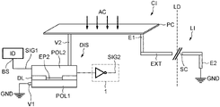
- FIG. 2 shows an example of an integrated circuit
- FIG. 3 is a simplified depiction of said integrated circuit
- FIG. 4 illustrates a flow chart of a method.
- FIG. 1 shows an example of an integrated antifuse device DIS formed on an isolation region 10 of a substrate, of shallow trench isolation (STI) or local oxide (LOCOS for local oxidation of silicon) type.
- STI shallow trench isolation
- LOCOS local oxide
- a first layer of heavily n-doped polycrystalline silicon POL 1 is covered on the right-hand side by a dielectric layer DL, for example a silicon oxide layer or an oxide-nitride-oxide layer, known to those skilled in the art by the acronym ONO.
- a dielectric layer DL for example a silicon oxide layer or an oxide-nitride-oxide layer, known to those skilled in the art by the acronym ONO.
- the dielectric layer DL comprises a first portion DL 1 , the thickness EP 1 of which is between 100 ⁇ and 200 ⁇ and a second portion DL 2 that is thinned with respect to the rest of the dielectric layer DL, the thickness EP 2 of which is between 15 ⁇ and 30 ⁇ .
- the dielectric layer DL is at least partly covered by a second layer of polycrystalline silicon POL 2 , which is preferably heavily n-doped.
- the antifuse device DIS also comprises two conductive vias V 1 and V 2 allowing terminals to be accessed. More specifically, the conductive via V 1 allows access to a contact on the first layer of polycrystalline silicon POL 1 and the conductive via V 2 allows access to a contact on the second layer of polycrystalline silicon POL 2 .
- a voltage is applied to the second layer of polycrystalline silicon POL 2 through the via V 2 forming a control terminal V 2 , and if said voltage is higher than a breakdown voltage CL of said antifuse device, which may be between 3 V and 7 V for a 90 nm technology node, then said dielectric layer DL becomes conductive at the site of the thinned portion DL 2 , thus forming a permanent conductive path between the first layer of polycrystalline silicon POL 1 and the second layer of polycrystalline silicon POL 2 .
- a breakdown voltage CL of said antifuse device which may be between 3 V and 7 V for a 90 nm technology node
- FIG. 2 shows an example of an integrated circuit CI that is located in a first zone Z 1 of a semiconductor wafer and is separated from a second zone Z 2 of the wafer by a cutting path LD.
- a substrate S of the wafer and of the integrated circuit comprises isolating regions 10 , for example shallow trench isolations or a local oxide.
- the circuit CI comprises, on its outer periphery, a sealing ring AT.
- This structure is advantageous because it provides sealtightness and hence allows the integrated circuit CI to be protected from the potential propagation of chips and splinters when cutting the wafer to allow the integrated circuits to be singulated.
- the integrated circuit CI may comprise several sealing rings AT on its periphery, these being arranged side-by-side so as to bolster sealtightness and thus better protect the integrated circuit CI.
- the sealing ring AT comprises here a contact 7 forming a wall and a first metal track PST that is located at a first metallization level M 1 of an interconnect portion (known to those skilled in the art by the acronym BEOL for back end of line) of the integrated circuit CI.
- the sealing ring AT rests on a first polysilicon bar 5 that is itself arranged on a first dielectric layer 20 , for example a silicon oxide layer or an oxide-nitride-oxide layer.
- the dielectric layer 20 separates the first polysilicon bar 5 from a second polysilicon bar 3 that is itself separated from the substrate S by a second dielectric layer 30 , for example a silicon oxide layer or an oxide-nitride-oxide layer.
- This stack of polysilicon bars and of oxide layers crosses the contact wall 7 and extends to the periphery of the integrated circuit CI.
- This crossing portion TRA constitutes a portion of an electrically conductive connecting element LI which therefore extends to the outside of the integrated circuit CI.
- the electrically conductive connecting element LI extends between a first site E 1 inside the integrated circuit CI and a second site E 2 located outside the integrated circuit CI (in this case a site on the substrate that is located in zone Z 2 of the wafer beyond the cutting line LD).
- the connecting element LI also comprises a straddling portion PST 2 that will straddle said cutting line LD.
- the straddling portion is located at the first metallization level M 1 .
- the straddling portion PST 2 is connected to the second location E 2 by a contact 73 that is arranged on a first metal silicide layer 81 .
- the straddling portion PST 2 is connected to the second polycrystalline silicon bar 3 by the contact 72 that is arranged on a second metal silicide layer 82 .
- the first site E 1 is connected to an electrically conductive body PC through a via 71 resting on a third metal silicide layer 83 .
- the body PC is located here at the metallization level M 1 but it could advantageously be located at a higher metallization level.
- the electrically conductive body PC is coupled to said antifuse device DIS by the via or the control terminal V 2 .
- the electrically conductive body PC may comprise an electrically conductive wafer.
- the second site E 2 thus connected to the substrate S by the first metal silicide layer 81 makes it possible, if the substrate S is kept grounded, to keep the first site E 1 and hence the electrically conductive body PC grounded.
- this is particularly advantageous for shedding electric charge that might build up on the wafer PC during the production of the integrated circuit.
- the straddling portion PST 2 of the connecting element LI will subsequently be cut through, thus conferring a discharged state on said body PC.
- the body PC becomes an electrically conductive body at a floating potential holding here an electrically zero initial amount of charge.
- connecting element passing through the sealing ring is particularly advantageous because it allows the conductive body PC to be kept grounded while protecting the integrated circuit from the intrusion of interfering external elements. That being said, other configurations of the connecting element are possible without necessarily passing through the sealing ring. For example, it is possible to envisage a connection between an upper contact pad of the integrated circuit, connected to the conductive body and the second site E 2 , passing over the sealing ring AT.
- FIG. 3 is a simplified depiction of said integrated circuit CI after cutting through SC the straddling portion PST 2 .
- the connecting element LI comprises a free end EXT that is located outside said sealing ring AT.
- free end is understood to mean that there is no longer any contact between the integrated circuit CI and an external element.
- the integrated circuit CI therefore comprises said electrically conductive body PC at a floating potential that is intended to receive electric charge AC during an electron beam attack, coupled to said antifuse device DIS by the control terminal V 2 .
- the integrated circuit CI also comprises a module ID, for example a register, a memory or an electronic circuit, that is configured to transmit, via its output BS, data SIG 1 to one or more other modules 1 , for example another memory or a state machine of the integrated circuit.
- the output BS of the module ID is coupled to the antifuse device DIS by the second layer of polycrystalline silicon POL 2 , just like the module 1 .
- the antifuse device DIS and more particularly the second layer of polycrystalline silicon, is configured to transmit data SIG 1 sent by the module ID to the inverter at the other module 1 .
- the antifuse device is also coupled to ground GND by the terminal V 1 of the first layer of polycrystalline silicon POL 1 .
- the data SIG 1 cannot go to ground since the dielectric layer DL separates the first layer of polycrystalline silicon POL 1 and the second layer of polycrystalline silicon POL 2 (the antifuse device is in its first state corresponding to an open circuit between the terminal V 1 and the second layer POL 2 ).
- FIG. 4 illustrates a flow chart of the method according to one implementation.
- Step 100 comprises the application of a voltage to the terminal V 2 resulting from a buildup of electric charge on said electrically conductive body PC.
- the antifuse device remains in the first state corresponding to an open circuit.
- the data SIG 1 from the module ID continue to be transmitted to the module 1 by passing through the second layer of polycrystalline silicon POL 2 .
- step 120 said permanent electrically conductive path between the first layer of polycrystalline silicon POL 1 and the second layer of polycrystalline silicon POL 2 .
- the output BS of the module ID is therefore connected to ground, thereby making the data contained in or processed by the module ID inaccessible.
Landscapes
- Engineering & Computer Science (AREA)
- Computer Hardware Design (AREA)
- Computer Security & Cryptography (AREA)
- General Engineering & Computer Science (AREA)
- Microelectronics & Electronic Packaging (AREA)
- Physics & Mathematics (AREA)
- General Physics & Mathematics (AREA)
- Theoretical Computer Science (AREA)
- Semiconductor Integrated Circuits (AREA)
- Design And Manufacture Of Integrated Circuits (AREA)
Applications Claiming Priority (2)
| Application Number | Priority Date | Filing Date | Title |
|---|---|---|---|
| FR1856887 | 2018-07-25 | ||
| FR1856887A FR3084521B1 (fr) | 2018-07-25 | 2018-07-25 | Procede de protection d'un module de circuit integre et dispositif correspondant |
Publications (2)
| Publication Number | Publication Date |
|---|---|
| US20200035671A1 US20200035671A1 (en) | 2020-01-30 |
| US11367720B2 true US11367720B2 (en) | 2022-06-21 |
Family
ID=65685436
Family Applications (1)
| Application Number | Title | Priority Date | Filing Date |
|---|---|---|---|
| US16/518,436 Active 2040-04-23 US11367720B2 (en) | 2018-07-25 | 2019-07-22 | Method for protecting an integrated circuit module using an antifuse, and corresponding device |
Country Status (2)
| Country | Link |
|---|---|
| US (1) | US11367720B2 (fr) |
| FR (1) | FR3084521B1 (fr) |
Citations (22)
| Publication number | Priority date | Publication date | Assignee | Title |
|---|---|---|---|---|
| EP1293988A2 (fr) | 2001-09-14 | 2003-03-19 | Hewlett-Packard Company | Cellule de mémoire |
| EP1400887A1 (fr) * | 2002-09-20 | 2004-03-24 | EM Microelectronic-Marin SA | Dispositif de protection pour puce électronique comportant des informations confidentielles |
| US6856581B1 (en) | 2000-10-31 | 2005-02-15 | International Business Machines Corporation | Batteryless, oscillatorless, binary time cell usable as an horological device with associated programming methods and devices |
| US20050104161A1 (en) * | 2003-11-18 | 2005-05-19 | Matsushita Electric Industrial Co., Ltd. | Semiconductor wafer |
| US20050201158A1 (en) | 2002-08-27 | 2005-09-15 | Stmicroelectronics Sa | EEPROM memory comprising a non-volatile register integrated into the memory array thereof |
| US20060028340A1 (en) | 2004-08-04 | 2006-02-09 | Hooghan Kultaransingh N | Method and apparatus for disabling an integrated circuit (IC) when an attempt is made to bypass security on the IC |
| US20060090211A1 (en) * | 2003-01-10 | 2006-04-27 | Koninklijke Phillips Electronics N.C. | Circuit arrangement and method for protecting electronic components against illicit manipulation |
| FR2938953A1 (fr) | 2008-11-21 | 2010-05-28 | Innova Card | Dispositif de protection d'un boitier de circuit integre electronique contre les intrusions par voie physique ou chimique. |
| US8022460B2 (en) | 2006-03-31 | 2011-09-20 | Semiconductor Energy Laboratory Co., Ltd. | Nonvolatile semiconductor memory device |
| US8304313B2 (en) | 2004-08-23 | 2012-11-06 | Semiconductor Energy Laboratory Co., Ltd. | Semiconductor device and its manufacturing method |
| US20130032926A1 (en) * | 2011-08-01 | 2013-02-07 | Fornara Pascal | Adjustable resistor |
| US8378710B1 (en) | 2011-09-20 | 2013-02-19 | Nxp B.V. | Secure device anti-tampering circuit |
| US20130134499A1 (en) | 2011-11-30 | 2013-05-30 | Kosuke Tatsumura | Nonvolatile programmable switches |
| FR2985059A1 (fr) * | 2011-12-21 | 2013-06-28 | Oberthur Technologies | Dispositif de securisation d'un document electronique |
| US20130193437A1 (en) | 2012-01-27 | 2013-08-01 | Stmicroelectronics (Rousset) Sas | Device for protecting an integrated circuit against back side attacks |
| US20130314121A1 (en) | 2012-05-24 | 2013-11-28 | Stmicroelectronics (Grenoble 2) Sas | Method and device for protecting an integrated circuit against backside attacks |
| EP2680184A1 (fr) | 2012-06-27 | 2014-01-01 | EM Microelectronic-Marin SA | Circuit intégré protégé contre des intrusions d'un pirate |
| US20140375303A1 (en) | 2012-01-06 | 2014-12-25 | Technische Universitaet Berlin | Charge measuring device |
| US9025373B2 (en) | 2012-07-17 | 2015-05-05 | Kabushiki Kaisha Toshiba | Non-volatile programmable switch |
| US20160042199A1 (en) | 2014-08-06 | 2016-02-11 | Maxim Integrated Products, Inc. | Detecting and thwarting backside attacks on secured systems |
| US20160328578A1 (en) | 2014-01-08 | 2016-11-10 | Stc.Unm | Systems and methods for generating physically unclonable functions from non-volatile memory cells |
| US20200035624A1 (en) | 2018-07-30 | 2020-01-30 | Stmicroelectronics (Rousset) Sas | Method for detecting an attack by means of a beam of electrically charged particles on an integrated circuit, and corresponding integrated circuit |
-
2018
- 2018-07-25 FR FR1856887A patent/FR3084521B1/fr active Active
-
2019
- 2019-07-22 US US16/518,436 patent/US11367720B2/en active Active
Patent Citations (23)
| Publication number | Priority date | Publication date | Assignee | Title |
|---|---|---|---|---|
| US6856581B1 (en) | 2000-10-31 | 2005-02-15 | International Business Machines Corporation | Batteryless, oscillatorless, binary time cell usable as an horological device with associated programming methods and devices |
| EP1293988A2 (fr) | 2001-09-14 | 2003-03-19 | Hewlett-Packard Company | Cellule de mémoire |
| US20050201158A1 (en) | 2002-08-27 | 2005-09-15 | Stmicroelectronics Sa | EEPROM memory comprising a non-volatile register integrated into the memory array thereof |
| EP1400887A1 (fr) * | 2002-09-20 | 2004-03-24 | EM Microelectronic-Marin SA | Dispositif de protection pour puce électronique comportant des informations confidentielles |
| US20060090211A1 (en) * | 2003-01-10 | 2006-04-27 | Koninklijke Phillips Electronics N.C. | Circuit arrangement and method for protecting electronic components against illicit manipulation |
| US20050104161A1 (en) * | 2003-11-18 | 2005-05-19 | Matsushita Electric Industrial Co., Ltd. | Semiconductor wafer |
| US20060028340A1 (en) | 2004-08-04 | 2006-02-09 | Hooghan Kultaransingh N | Method and apparatus for disabling an integrated circuit (IC) when an attempt is made to bypass security on the IC |
| US8304313B2 (en) | 2004-08-23 | 2012-11-06 | Semiconductor Energy Laboratory Co., Ltd. | Semiconductor device and its manufacturing method |
| US8022460B2 (en) | 2006-03-31 | 2011-09-20 | Semiconductor Energy Laboratory Co., Ltd. | Nonvolatile semiconductor memory device |
| FR2938953A1 (fr) | 2008-11-21 | 2010-05-28 | Innova Card | Dispositif de protection d'un boitier de circuit integre electronique contre les intrusions par voie physique ou chimique. |
| US20130032926A1 (en) * | 2011-08-01 | 2013-02-07 | Fornara Pascal | Adjustable resistor |
| US8729668B2 (en) | 2011-08-01 | 2014-05-20 | Stmicroelectronics (Rousset) Sas | Adjustable resistor |
| US8378710B1 (en) | 2011-09-20 | 2013-02-19 | Nxp B.V. | Secure device anti-tampering circuit |
| US20130134499A1 (en) | 2011-11-30 | 2013-05-30 | Kosuke Tatsumura | Nonvolatile programmable switches |
| FR2985059A1 (fr) * | 2011-12-21 | 2013-06-28 | Oberthur Technologies | Dispositif de securisation d'un document electronique |
| US20140375303A1 (en) | 2012-01-06 | 2014-12-25 | Technische Universitaet Berlin | Charge measuring device |
| US20130193437A1 (en) | 2012-01-27 | 2013-08-01 | Stmicroelectronics (Rousset) Sas | Device for protecting an integrated circuit against back side attacks |
| US20130314121A1 (en) | 2012-05-24 | 2013-11-28 | Stmicroelectronics (Grenoble 2) Sas | Method and device for protecting an integrated circuit against backside attacks |
| EP2680184A1 (fr) | 2012-06-27 | 2014-01-01 | EM Microelectronic-Marin SA | Circuit intégré protégé contre des intrusions d'un pirate |
| US9025373B2 (en) | 2012-07-17 | 2015-05-05 | Kabushiki Kaisha Toshiba | Non-volatile programmable switch |
| US20160328578A1 (en) | 2014-01-08 | 2016-11-10 | Stc.Unm | Systems and methods for generating physically unclonable functions from non-volatile memory cells |
| US20160042199A1 (en) | 2014-08-06 | 2016-02-11 | Maxim Integrated Products, Inc. | Detecting and thwarting backside attacks on secured systems |
| US20200035624A1 (en) | 2018-07-30 | 2020-01-30 | Stmicroelectronics (Rousset) Sas | Method for detecting an attack by means of a beam of electrically charged particles on an integrated circuit, and corresponding integrated circuit |
Non-Patent Citations (1)
| Title |
|---|
| INPI Search Report and Written Opinion for FR 1856887 dated Apr. 3, 2019 (10 pages). |
Also Published As
| Publication number | Publication date |
|---|---|
| FR3084521A1 (fr) | 2020-01-31 |
| US20200035671A1 (en) | 2020-01-30 |
| FR3084521B1 (fr) | 2020-08-14 |
Similar Documents
| Publication | Publication Date | Title |
|---|---|---|
| KR100416860B1 (ko) | 앤티퓨즈 및 그 형성 방법 | |
| EP0693781B1 (fr) | Procédé avec mise à la masse pour éliminer l'effet d'antenne pendant la fabrication | |
| US5393701A (en) | Layout design to eliminate process antenna effect | |
| US6815771B2 (en) | Silicon on insulator device and layout method of the same | |
| US7129545B2 (en) | Charge modulation network for multiple power domains for silicon-on-insulator technology | |
| US10943876B2 (en) | Method for detecting an attack by means of a beam of electrically charged particles on an integrated circuit, and corresponding integrated circuit | |
| JP2009532885A (ja) | ハイブリッド配向トランジスタにおける帯電損傷からの保護 | |
| US6836000B1 (en) | Antifuse structure and method of use | |
| US11942440B2 (en) | Method for detecting a differential fault analysis attack and a thinning of the substrate in an integrated circuit, and associated integrated circuit | |
| US10886283B2 (en) | Compact antifuse element and fabrication process | |
| US11322503B2 (en) | Integrated circuit including at least one memory cell with an antifuse device | |
| US11367720B2 (en) | Method for protecting an integrated circuit module using an antifuse, and corresponding device | |
| JP3273001B2 (ja) | 半導体記憶装置とその製造方法 | |
| US6297984B1 (en) | Structure and method for protecting integrated circuits during plasma processing | |
| JPH11306786A (ja) | 自己破壊型半導体装置 | |
| US11715705B2 (en) | Method for protecting data stored in a memory, and corresponding integrated circuit | |
| US5661331A (en) | Fuse bank | |
| US11270957B2 (en) | Method for detecting a breach of the integrity of a semiconductor substrate of an integrated circuit from its rear face, and corresponding device | |
| US11329011B2 (en) | Method for protecting an integrated circuit, and corresponding device | |
| CN101107709A (zh) | 防攻击保护的电子元件 | |
| JP3795798B2 (ja) | 半導体記憶装置 | |
| US20040222454A1 (en) | Semiconductor device and method for manufacturing the same | |
| KR19990057946A (ko) | 반도체 장치의 보호 회로 | |
| JP2003100990A (ja) | 絶縁膜破壊型フューズ | |
| MXPA01001738A (en) | Semiconductor chip with surface coating |
Legal Events
| Date | Code | Title | Description |
|---|---|---|---|
| AS | Assignment |
Owner name: STMICROELECTRONICS (ROUSSET) SAS, FRANCE Free format text: ASSIGNMENT OF ASSIGNORS INTEREST;ASSIGNORS:FORNARA, PASCAL;MARINET, FABRICE;SIGNING DATES FROM 20190514 TO 20190516;REEL/FRAME:049822/0305 |
|
| FEPP | Fee payment procedure |
Free format text: ENTITY STATUS SET TO UNDISCOUNTED (ORIGINAL EVENT CODE: BIG.); ENTITY STATUS OF PATENT OWNER: LARGE ENTITY |
|
| STPP | Information on status: patent application and granting procedure in general |
Free format text: DOCKETED NEW CASE - READY FOR EXAMINATION |
|
| STPP | Information on status: patent application and granting procedure in general |
Free format text: NON FINAL ACTION MAILED |
|
| STPP | Information on status: patent application and granting procedure in general |
Free format text: RESPONSE TO NON-FINAL OFFICE ACTION ENTERED AND FORWARDED TO EXAMINER |
|
| STPP | Information on status: patent application and granting procedure in general |
Free format text: NON FINAL ACTION MAILED |
|
| STPP | Information on status: patent application and granting procedure in general |
Free format text: RESPONSE TO NON-FINAL OFFICE ACTION ENTERED AND FORWARDED TO EXAMINER |
|
| STPP | Information on status: patent application and granting procedure in general |
Free format text: NOTICE OF ALLOWANCE MAILED -- APPLICATION RECEIVED IN OFFICE OF PUBLICATIONS |
|
| STPP | Information on status: patent application and granting procedure in general |
Free format text: PUBLICATIONS -- ISSUE FEE PAYMENT VERIFIED |
|
| STCF | Information on status: patent grant |
Free format text: PATENTED CASE |
|
| MAFP | Maintenance fee payment |
Free format text: PAYMENT OF MAINTENANCE FEE, 4TH YEAR, LARGE ENTITY (ORIGINAL EVENT CODE: M1551); ENTITY STATUS OF PATENT OWNER: LARGE ENTITY Year of fee payment: 4 |