US11600761B2 - High critical temperature metal nitride layer with oxide or oxynitride seed layer - Google Patents
High critical temperature metal nitride layer with oxide or oxynitride seed layer Download PDFInfo
- Publication number
- US11600761B2 US11600761B2 US17/178,187 US202117178187A US11600761B2 US 11600761 B2 US11600761 B2 US 11600761B2 US 202117178187 A US202117178187 A US 202117178187A US 11600761 B2 US11600761 B2 US 11600761B2
- Authority
- US
- United States
- Prior art keywords
- seed layer
- metal
- layer
- nitride
- oxynitride
- Prior art date
- Legal status (The legal status is an assumption and is not a legal conclusion. Google has not performed a legal analysis and makes no representation as to the accuracy of the status listed.)
- Active, expires
Links
Images


Classifications
-
- H01L39/12—
-
- G—PHYSICS
- G01—MEASURING; TESTING
- G01J—MEASUREMENT OF INTENSITY, VELOCITY, SPECTRAL CONTENT, POLARISATION, PHASE OR PULSE CHARACTERISTICS OF INFRARED, VISIBLE OR ULTRAVIOLET LIGHT; COLORIMETRY; RADIATION PYROMETRY
- G01J1/00—Photometry, e.g. photographic exposure meter
- G01J1/42—Photometry, e.g. photographic exposure meter using electric radiation detectors
-
- H—ELECTRICITY
- H10—SEMICONDUCTOR DEVICES; ELECTRIC SOLID-STATE DEVICES NOT OTHERWISE PROVIDED FOR
- H10N—ELECTRIC SOLID-STATE DEVICES NOT OTHERWISE PROVIDED FOR
- H10N60/00—Superconducting devices
- H10N60/80—Constructional details
- H10N60/85—Superconducting active materials
-
- H01L39/223—
-
- H—ELECTRICITY
- H10—SEMICONDUCTOR DEVICES; ELECTRIC SOLID-STATE DEVICES NOT OTHERWISE PROVIDED FOR
- H10N—ELECTRIC SOLID-STATE DEVICES NOT OTHERWISE PROVIDED FOR
- H10N60/00—Superconducting devices
- H10N60/01—Manufacture or treatment
- H10N60/0241—Manufacture or treatment of devices comprising nitrides or carbonitrides
-
- H—ELECTRICITY
- H10—SEMICONDUCTOR DEVICES; ELECTRIC SOLID-STATE DEVICES NOT OTHERWISE PROVIDED FOR
- H10N—ELECTRIC SOLID-STATE DEVICES NOT OTHERWISE PROVIDED FOR
- H10N60/00—Superconducting devices
- H10N60/10—Junction-based devices
- H10N60/12—Josephson-effect devices
-
- H—ELECTRICITY
- H10—SEMICONDUCTOR DEVICES; ELECTRIC SOLID-STATE DEVICES NOT OTHERWISE PROVIDED FOR
- H10N—ELECTRIC SOLID-STATE DEVICES NOT OTHERWISE PROVIDED FOR
- H10N60/00—Superconducting devices
- H10N60/20—Permanent superconducting devices
-
- H—ELECTRICITY
- H10—SEMICONDUCTOR DEVICES; ELECTRIC SOLID-STATE DEVICES NOT OTHERWISE PROVIDED FOR
- H10N—ELECTRIC SOLID-STATE DEVICES NOT OTHERWISE PROVIDED FOR
- H10N60/00—Superconducting devices
- H10N60/80—Constructional details
- H10N60/84—Switching means for devices switchable between superconducting and normal states
-
- G—PHYSICS
- G01—MEASURING; TESTING
- G01J—MEASUREMENT OF INTENSITY, VELOCITY, SPECTRAL CONTENT, POLARISATION, PHASE OR PULSE CHARACTERISTICS OF INFRARED, VISIBLE OR ULTRAVIOLET LIGHT; COLORIMETRY; RADIATION PYROMETRY
- G01J1/00—Photometry, e.g. photographic exposure meter
- G01J1/42—Photometry, e.g. photographic exposure meter using electric radiation detectors
- G01J1/44—Electric circuits
- G01J2001/4413—Type
- G01J2001/442—Single-photon detection or photon counting
-
- G—PHYSICS
- G02—OPTICS
- G02B—OPTICAL ELEMENTS, SYSTEMS OR APPARATUS
- G02B6/00—Light guides; Structural details of arrangements comprising light guides and other optical elements, e.g. couplings
- G02B6/10—Light guides; Structural details of arrangements comprising light guides and other optical elements, e.g. couplings of the optical waveguide type
- G02B6/12—Light guides; Structural details of arrangements comprising light guides and other optical elements, e.g. couplings of the optical waveguide type of the integrated circuit kind
Definitions
- the disclosure concerns use of a seed layer to improve the superconducting critical temperature of a metal nitride layer.
- the critical temperature refers to the temperature below which a material becomes superconductive.
- Niobium nitride is a material that can be used for superconducting applications, e.g., superconducting nanowire single photon detectors (SNSPD) for use in quantum information processing, defect analysis in CMOS, LIDAR, etc.
- SNSPD superconducting nanowire single photon detectors
- the critical temperature of niobium nitride depends on the crystalline structure and atomic ratio of the material. For example, referring to FIG. 1 , cubic ⁇ -phase NbN has some advantages due to its relatively “high” critical temperature, e.g., 9.7-16.5 K (the indicated process temperatures are for a particular fabrication process, and not necessarily applicable other process and deposition chamber designs).
- Niobium nitride can be deposited on a workpiece by physical vapor deposition (PVD).
- PVD physical vapor deposition
- a sputtering operation can be performed using a niobium target in the presence of nitrogen gas.
- the sputtering can be performed by inducing a plasma in the reactor chamber that contains the target and the workpiece.
- a superconducting device in one aspect, includes a substrate, a metal oxide or metal oxynitride seed layer on the substrate, and a metal nitride superconductive layer disposed directly on the seed layer.
- the seed layer is an oxide or oxynitride of a first metal
- the superconductive layer is a nitride of a different second metal.
- a superconducting device in another aspect, includes a substrate, a lower seed layer on the substrate, an upper seed layer disposed directly on the lower seed layer, and a superconductive layer disposed directly on the upper seed layer.
- the lower seed layer is a nitride of a first metal
- the upper seed layer is an oxide or oxynitride of the first metal
- the superconductive layer is a nitride of a different second metal.
- Implementations may provide, but are not limited to, one or more of the following advantages.
- the critical temperature of the metal nitride layer e.g., the NbN layer, can be increased. This permits fabrication of devices, e.g., SNSPDs, with superconductive wires with a higher critical temperature.
- the larger difference between the operating temperature (2-3 K) and the critical temperature provides superior detection efficiency, lower dark count, and possibly faster temporal response.
- “superconductive” indicates that the material becomes superconducting at the operating temperature of the device, e.g., 2-3° K. The material is not actually superconducting during fabrication of the device at or above room temperature or when the device is not being cooled for operation.
- FIG. 1 diagram illustrating phase of niobium nitride as a function of processing temperature and atomic percentage nitrogen.
- FIG. 2 A is a schematic cross-sectional view of a device that includes a metal nitride lower seed layer, a metal oxide or oxynitride upper seed layer, and a superconductive metal nitride layer.
- FIG. 2 B is a schematic cross-sectional view of the device of FIG. 2 A in which the superconductive layer has been etched to form superconductive wires.
- FIGS. 3 A- 3 C are flow charts of a method of fabricating the device of FIG. 2 A or 2 B .
- FIG. 4 A is a schematic cross-sectional view of a device that includes a metal oxide or oxynitride seed layer and a superconductive metal nitride layer.
- FIG. 4 B is a schematic cross-sectional view of the device of FIG. 4 A in which the superconductive layer has been etched to form superconductive wires.
- FIG. 5 is a flow chart of a method of fabricating the device of FIG. 4 A or 4 B .
- FIG. 6 A is a schematic cross-sectional view of a device that includes a metal nitride seed layer and a superconductive metal nitride layer.
- FIG. 6 B is a schematic cross-sectional view of the device of FIG. 6 A in which the superconductive layer has been etched to form superconductive wires.
- FIG. 7 is a flow chart of a method of fabricating the device of FIG. 6 A or 6 B .
- FIG. 8 A is a schematic top view of a SNSPD that includes a distributed Bragg reflector.
- FIG. 8 B is a schematic cross-sectional side view of the device of FIG. 8 A .
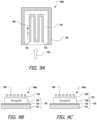
- FIG. 9 A is a schematic top view of a SNSPD that includes a waveguide.
- FIG. 9 B is a schematic cross-sectional side view of the device of FIG. 9 A .
- FIG. 9 C is a schematic cross-sectional side view of another implementation of the device of FIG. 9 A .
- niobium nitride particularly ⁇ -phase NbN
- ⁇ -phase NbN can be difficult to deposit at a satisfactory quality.
- the larger difference between the operating temperature (2-3 K) and the critical temperature the better the device performance.
- An aluminum nitride (AlN) layer can be used as a seed layer to improve the critical temperature of the NbN layer.
- AlN seed layer may induce a crystalline structure in the NbN layer that provides an increased critical temperature.
- exposure of the AlN seed layer to atmosphere and at room temperature before deposition of the NbN layer can actually provide a higher critical temperature, e.g., by about 0.5 K, than performing deposition of the NbN layer on the AlN seed layer without breaking vacuum and reducing the substrate temperature.
- a higher critical temperature e.g., by about 0.5 K
- two non-exclusive possibilities have been proposed.
- exposure of the AlN to atmosphere may result in the formation of a thin aluminum oxide or aluminum oxynitride layer on the surface of the AlN layer, which induces a superior crystalline structure in the NbN layer.
- thermally cycling the AlN seed layer by reducing the temperature of the substrate from a first deposition temperature for the AlN, e.g., 400° C., to room temperature, i.e., 20-22° C., and then raising the temperature of the substrate back to a second deposition temperature for the NbN, e.g., 400° C., may affect stress in the AlN seed layer which may affect its crystalline structure, which in turn can affect the crystalline structure of the NbN layer.
- a first deposition temperature for the AlN e.g. 400° C.
- room temperature i.e., 20-22° C.
- second deposition temperature for the NbN e.g. 400° C.
- FIG. 2 A is a schematic illustration of some layers in a device 100 that includes a metal nitride layer 108 for use as a superconductive material.
- FIG. 2 B is a schematic illustration of a device 100 in which the metal nitride layer has been formed into features, e.g., superconductive wires 108 ′.
- the device 100 could be superconducting nanowire single photon detectors (SNSPD), a superconducting quantum interference device (SQUID), a circuit, e.g., an RF line, in a quantum computer, etc.
- FIGS. 3 A- 3 C are flowcharts of methods 200 of fabrication.
- the metal nitride layer 108 is disposed on a support structure 102 .
- the support structure 102 can include a substrate, e.g., a silicon wafer.
- the substrate can be a dielectric material, e.g., sapphire, SiO 2 , fused silica, or quartz, or a semiconductor material, e.g., silicon, gallium nitride (GaN) or gallium arsenide (GaAs).
- the support structure 102 could include multiple underlying layers.
- the support structure 102 can include a distributed Bragg reflector (DBR) that includes multiple pairs of layers formed of high refractive index and low refractive index materials deposited over the substrate, or a waveguide formed on the substrate.
- DBR distributed Bragg reflector
- a seed layer structure 103 is formed over the support structure 102 .
- the seed layer structure 103 includes a lower layer seed layer 104 and an upper layer seed layer 106 .
- the lower seed layer 104 is a metal nitride layer.
- the lower seed layer 104 and the superconductive layer 108 are nitrides of different metals.
- the lower seed layer 104 can be aluminum nitride (AlN).
- AlN aluminum nitride
- the lower seed layer 104 can have a thickness of about 3 to 50 nm, e.g., about 5 nm or about 10 nm or about 20 nm thickness.
- the lower seed layer 104 can have a (002) c-axis crystal orientation.
- the lower seed layer 104 need not be superconducting at the operating temperature of the device 100 .
- the lower seed layer 104 can be deposited (step 202 ) by a standard chemical vapor deposition or physical vapor deposition process. The deposition process can be conducted with the substrate at a temperature of 200-500° C., e.g., 400° C.
- Exemplary processing parameters for the lower seed layer are a power applied to the sputtering target of 1-5 kW, a total pressure (nitrogen and inert gas) of 2 to 20 mTorr with nitrogen gas and inert gas supplied at a ratio between 3:100 and 6:1, e.g., about 3:1, a wafer temperature of 200-500° C., and no bias voltage applied to the wafer.
- the upper seed layer 106 is a metal oxide or metal oxynitride layer.
- the upper seed layer 106 is an oxide or oxynitride of the same metal as the metal of the metal nitride in the lower seed layer 104 .
- the upper seed layer 106 can be aluminum oxide or aluminum oxynitride, as this appears to improve the critical temperature of NbN, e.g., by about 0.5 K over aluminum nitride as a seed layer.
- hafnium oxide or oxynitride, chromium oxide or oxynitride, or an oxide or oxynitride of an alloy of aluminum and either hafnium or scandium might also be suitable.
- the upper seed layer 106 can be thinner than the lower seed layer 104 .
- the upper seed layer 106 can be about 0.1-3 nm thick, depending on the method of fabrication. In some implementations, the upper seed layer 106 is only one to five atomic layers thick, e.g., two or three atomic layers thick.
- the upper seed layer 106 can have a (002) c-axis crystal orientation. The upper seed layer 106 need not be superconducting at the operating temperature of the device 100 .
- one technique that can be used to form the metal oxide or metal oxynitride of the upper seed layer 106 is to expose the lower seed layer 104 to a gas containing oxygen and/or water (step 204 a ).
- the lower seed layer 104 can be exposed to air.
- the lower seed layer 104 could be exposed to pure oxygen.
- the lower seed layer 104 could be exposed to a gas mixture containing oxygen at 20-90% by volume and one or more other gases, such nitrogen and/or a noble gas, e.g., argon.
- the gas mixture includes water, e.g., water vapor or steam.
- the pressure can be 1 Torr to 1 atmosphere, e.g., 0.8 to 1 atmosphere.
- another technique that can be used to form the metal oxide or metal oxynitride of the upper seed layer 106 is to expose the lower seed layer 104 to a gas containing oxygen (O 2 ) plasma (step 204 b ).
- the lower seed layer 104 could be exposed to pure oxygen plasma.
- oxygen gas can be directed into a plasma processing chamber, and an oxygen plasma can be formed at a power of about 100 W.
- the pressure can be 2 to 500 mTorr.
- a dedicated chamber for oxygen plasma treatment can use a relatively higher pressure, e.g., 100-500 mTorr, whereas a relatively lower pressure, e.g., 2 to 15 mTorr, can be used if the oxygen plasma treatment is performed in the same chamber that is used for the deposition of the lower seed layer.
- exposure of AlN to oxygen may result in the formation of a thermal oxide or thermal oxynitride layer, i.e., an aluminum oxide or aluminum oxynitride layer, on the surface of the AlN layer.
- the substrate with the lower seed layer is lowered from a first temperature at which the lower seed layer is deposited, e.g., 300-500° C., to a lower second temperature, e.g., 20-300° C.
- the lower seed layer is exposed to the oxygen-containing gas or plasma at the lower second temperature.
- the second temperature can be at least 200° C. lower than the first temperature.
- the second temperature can be room temperature, i.e., 20-22° C.
- the substrate is then raised to an elevated third temperature for deposition of the metal nitride of the superconductive layer.
- the substrate with the lower seed layer is maintained at an elevated temperature, e.g., at or above 300° C., e.g., at the same temperature at which the lower seed layer is deposited, e.g., 400° C., and the substrate is exposed to the oxygen-containing gas or plasma at the elevated temperature.
- an elevated temperature e.g., at or above 300° C., e.g., at the same temperature at which the lower seed layer is deposited, e.g., 400° C.
- the substrate with the lower seed layer is lowered from the first temperature to the second temperature, then raised up to elevated third temperature, e.g., at or above 300° C., e.g., 300-500° C., and the lower seed layer exposed to the oxygen-containing gas or plasma, at the elevated third temperature.
- elevated third temperature e.g., at or above 300° C., e.g., 300-500° C.
- the exposure time can depend on pressure and temperature, and can be from 1 second to 120 minutes.
- the exposure time for atmosphere at room temperature can be about 45 minutes.
- the exposure time for oxygen plasma with the substrate at the same temperature at which the lower seed layer is deposited, e.g., at about 400° C. can be about 30 seconds.
- the upper seed layer 106 is effectively a native oxide or native oxynitride formed on the underlying metal nitride layer, and thus expected to be two to four atomic layers thick.
- the upper seed layer 106 can be up to about 1 nm thick.
- FIG. 3 C another technique that can be used to form the metal oxide or metal oxynitride of the upper seed layer 106 is to deposit the upper seed layer 106 by physical vapor deposition.
- Exemplary processing parameters for the upper seed layer are a power applied to the sputtering target of 1-5 kW, a total pressure (oxygen and inert gas) of 2 to 20 mTorr with oxygen gas and inert gas supplied at a ratio between 3:100 and 6:1, and a wafer temperature of 200-500° C.
- the thickness of the upper seed layer 106 depends on the processing time or number of iterations of the deposition process.
- the thickness of the upper seed layer 106 can be 1-2 nm.
- the superconductive metal nitride layer 108 is deposited (step 206 ) on, e.g., in direct contact with, the upper seed layer 106 .
- the metal nitride layer 108 is formed of niobium nitride (NbN), titanium nitride (TiN), or niobium titanium nitride (Nb x Ti 1-X N).
- the superconductive layer 108 can have a thickness of 4 to 50 nm, e.g., about 5 nm or about 10 nm or about 20 nm.
- the metal nitride layer 108 can be deposited using a standard chemical vapor deposition or physical vapor deposition process. Exemplary processing parameters are a base pressure of 1e-8 Torr, a power applied to the target of 1-3 kW, a total pressure during processing of 5-7 mTorr, a wafer temperature of 400° C., no bias voltage applied to the wafer, and a percentage of the gas as N 2 sufficient to achieve cubic ⁇ -phase NbN.
- the metal nitride layer 108 is deposited in the same processing chamber that is used to deposit the lower seed layer 104 and upper seed layer 106 , e.g., by switching in a new target. This permits higher throughput manufacturing.
- the substrate can be transported to a different deposition chamber without breaking vacuum. This permits the metal nitride layer to be deposited without exposure of the seed layer to atmosphere and with lower risk of contamination.
- a capping layer 110 can be deposited on the metal nitride layer 108 (step 208 ).
- the capping layer 110 serves as a protective layer, e.g., to prevent oxidation of the metal nitride layer 108 or other types of contamination or damage.
- the capping layer 108 can be dielectric but need not be superconductive at the operating temperature of the device 100 .
- the capping layer 108 can be amorphous silicon (a-Si).
- the capping layer 108 is a nitride of a different material from the metal of the metal nitride used for the superconductive layer 108 . Examples of materials for the capping layer 108 include AlN, Al 2 O 3 , SiO 2 , and SiN.
- the capping layer 108 can be deposited by a standard chemical vapor deposition or physical vapor deposition process.
- Etching can be used to form trenches 112 through at least the metal nitride layer 108 to form the superconductive wires 108 ′ or other structures needed for the device 100 (step 210 ).
- the wires 108 ′ can have a width of about 25 to 250 nm, e.g., about 60 nm.
- FIG. 2 B illustrates the trenches 112 as extending through the metal nitride layer 108 and capping layer 110 and not into the upper seed layer 106 , other configurations are possible. As an example, the trenches 112 can extend partially into or entirely through the upper seed layer 106 , or entirely through the upper seed layer 106 and partially into or entirely through the lower seed layer 104 .
- Air can contain contaminants, so for any of the above processes, the upper seed layer 106 can be formed on the lower seed layer 104 without breaking vacuum, e.g., without removing the substrate from the deposition chamber in which the lower seed layer is deposited, or without breaking vacuum during transfer of the substrate from the deposition chamber in which the lower seed layer is deposited to the chamber in which the upper seed layer is formed.
- the metal nitride superconductive layer 108 can be formed on the upper seed layer 106 without breaking vacuum.
- the upper seed layer 106 is formed by oxygen plasma treatment (see FIG. 3 B ) or by PVD (see FIG. 3 C )
- an Applied Materials Endura® with Impulse PVD could be used.
- the deposition of the lower seeding layer and either oxygen plasma treatment or PVD of an oxide or oxynitride could be performed within the same chamber.
- NbN deposition can be performed in a different chamber in the same Endura tool, but without breaking vacuum.
- FIG. 4 A is a schematic illustration of some layers in a device 100 ′ that includes a metal nitride layer 108 for use as a superconductive material.
- FIG. 4 B is a schematic illustration of a device 100 ′ in which the metal nitride layer has been formed into features, e.g., superconductive wires 108 ′.
- the device 100 ′ is similar to the device 100 , but instead of having both a lower seed layer and an upper seed layer, the seed layer structure 103 of device 100 ′ has a single metal oxide or metal oxynitride seed layer 106 ′. Except as discussed below, the device 100 ′ can be configured and manufactured as discussed with respect to device 100 .
- FIG. 5 is a flowchart of a method 200 ′ of fabrication.
- a seed layer 106 ′ is disposed on top of the support structure 102 .
- the seed layer 106 ′ is a metal oxide or metal oxynitride.
- the seed layer 106 ′ is an oxide or oxynitride of a different metal than the metal of the metal nitride in the superconductive layer 108 .
- the seed layer 106 ′ can be aluminum oxide or aluminum oxynitride (AlN), as this appears to improve the critical temperature of NbN, e.g., by about 0.5 K over aluminum nitride as a seed layer.
- AlN aluminum oxide or aluminum oxynitride
- hafnium oxide, hafnium oxynitride, gallium oxide, or gallium oxynitride might also be suitable.
- the seed layer 106 ′ can have a thickness of about 3 to 50 nm, e.g., about 5 nm or about 10 nm or about 20 nm thickness.
- the seed layer 106 ′ can have a (002) c-axis crystal orientation.
- the seed layer 106 ′ need not be superconducting at the operating temperature of the device 100 ′.
- the seed layer 106 ′ can be deposited (step 204 ′) by a standard chemical vapor deposition or physical vapor deposition process. The deposition process can be conducted with the substrate at a temperature of 200-500° C., e.g., 400° C.
- Exemplary processing parameters are a power applied to the sputtering target of 1-5 kW, a total pressure (nitrogen and inert gas) of 2 to 20 mTorr with nitrogen gas and inert gas supplied at a ratio between 3:100 and 1:6, a wafer temperature of 200-500° C., and no bias voltage applied to the wafer.
- An Applied Materials Endura® with Impulse PVD could be used for deposition of the seed layer and the superconductive layer.
- deposition of aluminum oxide can be performed in a first chamber, and NbN deposition can be performed in a different chamber in the same tool, but without breaking vacuum.
- Thermal cycling can be applied between the deposition of the seed layer 106 ′ and the superconductive layer 108 .
- the substrate with the seed layer 106 ′ is lowered from the first temperature to the second temperature, then raised up to elevated third temperature, e.g., at or above 300° C., e.g., 300-500° C., for deposition of the metal nitride superconductive layer 108 .
- the substrate with the seed layer 106 ′ can be maintained at an elevated temperature, e.g., at or above 300° C., e.g., at the same temperature at which the seed layer 106 ′ is deposited, e.g., 400° C., until deposition of the metal nitride superconductive layer 108 .
- FIG. 6 A is a schematic illustration of some layers in a device 100 ′′ that includes a metal nitride layer 108 for use as a superconductive material.
- FIG. 6 B is a schematic illustration of a device 100 ′′ in which the metal nitride layer has been formed into features, e.g., superconductive wires 108 ′.
- the device 100 ′′ is similar to the device 100 ′, but instead of having a seed layer of metal oxide or metal oxynitride, the seed layer structure 103 of device 100 ′′ includes a single layer of metal nitride that has been subjected to thermal cycling. Except as discussed below, the device 100 can be configured and manufactured as discussed with respect to devices 100 and 100 ′.
- FIG. 7 is a flowchart of a method 200 ′′ of fabrication.
- a seed layer 104 ′ is disposed on top of the support structure 102 .
- the seed layer 104 ′ is a metal nitride.
- the seed layer 104 ′ and the superconductive layer 108 are nitrides of different metals.
- the seed layer 104 ′ can be aluminum nitride. However, hafnium nitride or gallium nitride might also be suitable.
- the seed layer 104 ′ can be deposited (step 204 ′) directly on the support structure 102 by a standard chemical vapor deposition or physical vapor deposition process.
- the deposition process can be conducted with the substrate at a first temperature of 200-500° C., e.g., 400° C.
- the substrate with the metal nitride seed layer is subjected to thermal cycling (step 205 ).
- the substrate with the seed layer is lowered from the first temperature at which the seed layer is deposited, e.g., 200-500° C., to a lower second temperature.
- the substrate with the seed layer 104 ′ is lowered from the first temperature at which the seed layer is deposited, e.g., 300-500° C., to a lower second temperature, e.g., 20-300° C.
- the second temperature can be at least 200° C. lower than the first temperature.
- the second temperature can be room temperature, i.e., 20-22° C.
- the seed layer can be subject to thermal cycling while in vacuum, or while exposed to nitrogen and/or an inert gas, e.g., argon.
- the substrate is then raised to an elevated third temperature, e.g., e.g., 300-500° C., for deposition of the metal nitride of the superconductive layer. Thermally cycling may change the crystalline structure of the seed layer 104 ′.
- the metal nitride of the superconductive layer 108 can be deposited on the seed layer 104 ′.
- the superconductive layer 108 is deposited without breaking vacuum or otherwise exposing the seed layer to oxygen or an oxygen-containing vapor, e.g., H 2 O.
- FIGS. 8 A and 8 B illustrate top and side views, respectively, of a device 100 a configured as a superconducting nanowire single photon detector (SNSPD).
- the device 100 a can use any configuration of the seed layer 103 discussed above.
- the SNSPD device 100 a can include at least one superconductive wire 108 ′ disposed on a support structure 102 .
- the superconductive wire 108 ′ can be connected between conductive electrodes 120 .
- the superconductive wire 108 ′ can be arranged in a meandering pattern, e.g., a back-and-forth parallel lines, on the supporting structure 102 .
- multiple wires 108 ′ are connected in parallel between the electrodes 120 , with each wire 108 ′ covering a separate area 152 , but there could be just a single wire 108 ′ covering the entire detection area of the device 100 a .
- many other patterns are possible, e.g., zigzag or double spiral.
- the support structure 102 includes a substrate 124 and a distributed Bragg reflector (DBR) 126 that includes multiple pairs of layers formed of high refractive index and low refractive index materials.
- DBR distributed Bragg reflector
- the SNSPD device 100 a is operated with a photon (illustrated by light beam 10 a ) approaching from the top of the device 100 a , e.g., with normal incidence relative to the substrate 124 .
- the working principle of the SNSPD device is that the to-be-detected photon comes from top and shines on the SNPSD. Absorption of the photon, either on initial impingement or upon reflection from the DBR, creates a hot spot on the NbN nanowire which raises the temperature of the NbN above critical temperature so that a portion of the wire is no longer in the superconductive state. A region around the hot spot can experience current crowding, resulting in a higher current density than the critical current density, which can disrupt the superconductive state for the entire wire.
- the change in the NbN wire from the superconducting state to the normal resistive state can be electrically detected by flowing a current through the device and monitoring voltage differences between the electrodes.
- FIGS. 9 A and 9 B illustrate a device 100 b configured as a superconducting nanowire single photon detector (SNSPD) and having a waveguide 138 .
- the device 100 b can use any configuration of the seed layer 103 discussed above.
- the SNSPD device 100 b can include at least one superconductive wire 108 ′ disposed on a support structure 102 .
- the superconductive wire(s) 108 ′ can be arranged to form a plurality of parallel lines, with adjacent lines connected at alternating ends. Although FIG. 9 A illustrates four parallel lines, the device could have just two parallel lines, e.g., a U-shaped wire, or a greater number of lines.
- the superconductive wire 108 ′ can be connected between conductive electrodes.
- the support structure 102 can include a substrate 134 , a dielectric layer 136 on the substrate 134 , and a waveguide 138 disposed on the dielectric layer 136 .
- the dielectric layer 102 c is a first material having a first refractive index
- the waveguide 102 d is a second material having a second refractive index that is higher than the first refractive index.
- Photons shown by light beam 10 b , are injected into the device from the side, e.g., generally parallel to the top surface of the substrate 132 , through the waveguide 138 .
- the photons can enter along an axis (shown by arrow A) generally parallel to the parallel lines of the wire 108 ′.
- the wire 108 ′ can be located near the center of the waveguide 138 .
- This gap 130 can have a width of about 25-30% of the total width of the waveguide.
- the photons in the waveguide 138 are trapped by total internal reflection.
- the photons can escape into the nanowire 108 ′ and thus be absorbed by the nanowire 108 ′.
- the light coupling efficiency can be very high in this type of device.
- the top surface of the waveguide 138 can provide the lower seed layer and can be treated to form the upper seed layer 106 or the upper seed layer 106 can be formed directly on the waveguide 108 , i.e., without having to deposit a separate lower seed layer.
- an appropriate metal nitride e.g., aluminum nitride
Landscapes
- Engineering & Computer Science (AREA)
- Manufacturing & Machinery (AREA)
- Physics & Mathematics (AREA)
- General Physics & Mathematics (AREA)
- Spectroscopy & Molecular Physics (AREA)
- Superconductor Devices And Manufacturing Methods Thereof (AREA)
- Superconductors And Manufacturing Methods Therefor (AREA)
- Physical Vapour Deposition (AREA)
Priority Applications (2)
| Application Number | Priority Date | Filing Date | Title |
|---|---|---|---|
| US17/178,187 US11600761B2 (en) | 2020-02-21 | 2021-02-17 | High critical temperature metal nitride layer with oxide or oxynitride seed layer |
| US18/177,096 US12185643B2 (en) | 2020-02-21 | 2023-03-01 | High critical temperature metal nitride layer with oxide or oxynitride seed layer |
Applications Claiming Priority (2)
| Application Number | Priority Date | Filing Date | Title |
|---|---|---|---|
| US202062980079P | 2020-02-21 | 2020-02-21 | |
| US17/178,187 US11600761B2 (en) | 2020-02-21 | 2021-02-17 | High critical temperature metal nitride layer with oxide or oxynitride seed layer |
Related Child Applications (1)
| Application Number | Title | Priority Date | Filing Date |
|---|---|---|---|
| US18/177,096 Continuation US12185643B2 (en) | 2020-02-21 | 2023-03-01 | High critical temperature metal nitride layer with oxide or oxynitride seed layer |
Publications (2)
| Publication Number | Publication Date |
|---|---|
| US20220052248A1 US20220052248A1 (en) | 2022-02-17 |
| US11600761B2 true US11600761B2 (en) | 2023-03-07 |
Family
ID=77391802
Family Applications (2)
| Application Number | Title | Priority Date | Filing Date |
|---|---|---|---|
| US17/178,187 Active 2041-02-17 US11600761B2 (en) | 2020-02-21 | 2021-02-17 | High critical temperature metal nitride layer with oxide or oxynitride seed layer |
| US18/177,096 Active US12185643B2 (en) | 2020-02-21 | 2023-03-01 | High critical temperature metal nitride layer with oxide or oxynitride seed layer |
Family Applications After (1)
| Application Number | Title | Priority Date | Filing Date |
|---|---|---|---|
| US18/177,096 Active US12185643B2 (en) | 2020-02-21 | 2023-03-01 | High critical temperature metal nitride layer with oxide or oxynitride seed layer |
Country Status (5)
| Country | Link |
|---|---|
| US (2) | US11600761B2 (de) |
| EP (1) | EP4107794A4 (de) |
| JP (2) | JP7515602B2 (de) |
| TW (2) | TWI875958B (de) |
| WO (1) | WO2021168007A1 (de) |
Cited By (3)
| Publication number | Priority date | Publication date | Assignee | Title |
|---|---|---|---|---|
| US20230309420A1 (en) * | 2020-02-03 | 2023-09-28 | Applied Materials, Inc. | Snspd with integrated aluminum nitride seed or waveguide layer |
| US12052935B2 (en) | 2020-02-21 | 2024-07-30 | Applied Materials, Inc. | Method of making high critical temperature metal nitride layer |
| US12185643B2 (en) | 2020-02-21 | 2024-12-31 | Applied Materials, Inc. | High critical temperature metal nitride layer with oxide or oxynitride seed layer |
Citations (12)
| Publication number | Priority date | Publication date | Assignee | Title |
|---|---|---|---|---|
| US5477061A (en) | 1990-09-20 | 1995-12-19 | Fujitsu Limited | Josephson device having an overlayer structure with improved thermal stability |
| JPH1041558A (ja) | 1996-07-22 | 1998-02-13 | Sanyo Electric Co Ltd | 酸化物超電導デバイスの形成方法 |
| JP2003158306A (ja) | 2001-11-21 | 2003-05-30 | National Institute Of Advanced Industrial & Technology | 超伝導配線及びその作製方法 |
| JP2008112769A (ja) | 2006-10-30 | 2008-05-15 | National Institute Of Information & Communication Technology | 積層型超伝導接合及びその製造方法 |
| US20090312186A1 (en) * | 2007-10-12 | 2009-12-17 | Norem James H | Nano-fabricated superconducting radio-frequency composites, method for producing nano-fabricated superconducting rf composites |
| US20130084712A1 (en) | 2011-09-30 | 2013-04-04 | Hitachi Kokusai Electric Inc. | Method of manufacturing semiconductor device, method of processing substrate, substrate processing apparatus and non-transitory computer readable recording medium |
| US20150340841A1 (en) | 2009-02-17 | 2015-11-26 | Trilumina Corp | Laser arrays for variable optical properties |
| US20150372217A1 (en) | 2013-01-18 | 2015-12-24 | Yale University | Methods for making a superconducting device with at least one enclosure |
| JP2016213363A (ja) | 2015-05-12 | 2016-12-15 | 国立研究開発法人情報通信研究機構 | 超伝導トンネル接合素子の形成方法 |
| US20170148950A1 (en) | 2014-07-02 | 2017-05-25 | Aledia | Optoelectronic device having semiconductor elements and method for manufacturing same |
| US20200035481A1 (en) | 2018-07-26 | 2020-01-30 | Tokyo Electron Limited | Method of forming titanium nitride films with (200) crystallographic texture |
| US20220013707A1 (en) | 2020-02-21 | 2022-01-13 | Applied Materials, Inc. | Method of making high critical temperature metal nitride layer |
Family Cites Families (14)
| Publication number | Priority date | Publication date | Assignee | Title |
|---|---|---|---|---|
| US4589001A (en) | 1980-07-09 | 1986-05-13 | Agency Of Industrial Science & Technology | Quasiparticle injection control type superconducting device |
| JPS60169175A (ja) * | 1984-02-13 | 1985-09-02 | Rikagaku Kenkyusho | 弱結合ジョセフソン接合素子 |
| US4844989A (en) | 1987-03-19 | 1989-07-04 | The University Of Chicago (Arch Development Corp.) | Superconducting structure with layers of niobium nitride and aluminum nitride |
| JPH01307281A (ja) * | 1988-06-06 | 1989-12-12 | Tosoh Corp | ジョセフソン・ブリッジ素子 |
| JPH0239475A (ja) * | 1988-07-28 | 1990-02-08 | Tosoh Corp | ディーシースキッド |
| US8124176B2 (en) | 2000-07-31 | 2012-02-28 | Los Alamos National Security, Llc | Polymer-assisted deposition of films |
| US8659085B2 (en) | 2010-08-24 | 2014-02-25 | Stmicroelectronics Pte Ltd. | Lateral connection for a via-less thin film resistor |
| SG11201505616YA (en) | 2013-01-18 | 2015-09-29 | Univ Yale | Superconducting device with at least one enclosure |
| EP2821166B1 (de) | 2013-07-04 | 2016-04-20 | Sandvik Intellectual Property AB | Verfahren zur Herstellung einer verschleißbeständigen Komponente mit mechanisch gekoppelten zementierten Karbidkörpern |
| WO2019126564A1 (en) * | 2017-12-20 | 2019-06-27 | PsiQuantum Corp. | Complementary metal-oxide semiconductor compatible patterning of superconducting nanowire single-photon detectors |
| US10256392B1 (en) * | 2018-03-23 | 2019-04-09 | International Business Machines Corporation | Vertical transmon qubit device |
| US10320331B1 (en) * | 2018-07-30 | 2019-06-11 | International Business Machines Corporation | Applications of a superconducting device that mixes surface acoustic waves and microwave signals |
| US20200227618A1 (en) | 2019-01-14 | 2020-07-16 | Auburn University | Protective barrier layers for superconducting structures |
| EP4107794A4 (de) | 2020-02-21 | 2024-02-28 | Applied Materials, Inc. | Metallnitridschicht mit hoher kritischer temperatur mit einer oxid- oder oxynitridkeimschicht |
-
2021
- 2021-02-17 EP EP21756913.6A patent/EP4107794A4/de active Pending
- 2021-02-17 WO PCT/US2021/018414 patent/WO2021168007A1/en not_active Ceased
- 2021-02-17 US US17/178,187 patent/US11600761B2/en active Active
- 2021-02-17 JP JP2022549647A patent/JP7515602B2/ja active Active
- 2021-02-19 TW TW110105713A patent/TWI875958B/zh active
- 2021-02-19 TW TW114107105A patent/TW202527830A/zh unknown
-
2023
- 2023-03-01 US US18/177,096 patent/US12185643B2/en active Active
-
2024
- 2024-07-02 JP JP2024106850A patent/JP7821843B2/ja active Active
Patent Citations (14)
| Publication number | Priority date | Publication date | Assignee | Title |
|---|---|---|---|---|
| US5477061A (en) | 1990-09-20 | 1995-12-19 | Fujitsu Limited | Josephson device having an overlayer structure with improved thermal stability |
| JPH1041558A (ja) | 1996-07-22 | 1998-02-13 | Sanyo Electric Co Ltd | 酸化物超電導デバイスの形成方法 |
| JP2003158306A (ja) | 2001-11-21 | 2003-05-30 | National Institute Of Advanced Industrial & Technology | 超伝導配線及びその作製方法 |
| JP2008112769A (ja) | 2006-10-30 | 2008-05-15 | National Institute Of Information & Communication Technology | 積層型超伝導接合及びその製造方法 |
| US20090312186A1 (en) * | 2007-10-12 | 2009-12-17 | Norem James H | Nano-fabricated superconducting radio-frequency composites, method for producing nano-fabricated superconducting rf composites |
| US20150340841A1 (en) | 2009-02-17 | 2015-11-26 | Trilumina Corp | Laser arrays for variable optical properties |
| US20130084712A1 (en) | 2011-09-30 | 2013-04-04 | Hitachi Kokusai Electric Inc. | Method of manufacturing semiconductor device, method of processing substrate, substrate processing apparatus and non-transitory computer readable recording medium |
| US20150372217A1 (en) | 2013-01-18 | 2015-12-24 | Yale University | Methods for making a superconducting device with at least one enclosure |
| US20170148950A1 (en) | 2014-07-02 | 2017-05-25 | Aledia | Optoelectronic device having semiconductor elements and method for manufacturing same |
| JP2016213363A (ja) | 2015-05-12 | 2016-12-15 | 国立研究開発法人情報通信研究機構 | 超伝導トンネル接合素子の形成方法 |
| US20200035481A1 (en) | 2018-07-26 | 2020-01-30 | Tokyo Electron Limited | Method of forming titanium nitride films with (200) crystallographic texture |
| KR20200012804A (ko) | 2018-07-26 | 2020-02-05 | 도쿄엘렉트론가부시키가이샤 | (200) 결정질 조직을 갖는 질화티탄막의 형성 방법 |
| US20220013707A1 (en) | 2020-02-21 | 2022-01-13 | Applied Materials, Inc. | Method of making high critical temperature metal nitride layer |
| US20220013708A1 (en) | 2020-02-21 | 2022-01-13 | Applied Materials, Inc. | Method of making high critical temperature metal nitride layer |
Non-Patent Citations (3)
| Title |
|---|
| International Search Report and Written Opinion in International Appln. No. PCT/US2021/018414, dated Jun. 10, 2021, 7 pages. |
| Polakovic et al., "Room temperature deposition of superconducting niobium nitride films by ion beam assisted sputtering," APL Materials, Jul. 2018, 6(7):076107. |
| Wang et al., "Superconducting properties and crystal structures of single-crystal niobium nitride thin films deposited at ambient substrate temperature," Journal of Applied Science, May 1996, 79(10):7837-7842. |
Cited By (4)
| Publication number | Priority date | Publication date | Assignee | Title |
|---|---|---|---|---|
| US20230309420A1 (en) * | 2020-02-03 | 2023-09-28 | Applied Materials, Inc. | Snspd with integrated aluminum nitride seed or waveguide layer |
| US12317758B2 (en) * | 2020-02-03 | 2025-05-27 | Applied Materials, Inc. | SNSPD with integrated aluminum nitride seed or waveguide layer |
| US12052935B2 (en) | 2020-02-21 | 2024-07-30 | Applied Materials, Inc. | Method of making high critical temperature metal nitride layer |
| US12185643B2 (en) | 2020-02-21 | 2024-12-31 | Applied Materials, Inc. | High critical temperature metal nitride layer with oxide or oxynitride seed layer |
Also Published As
| Publication number | Publication date |
|---|---|
| US12185643B2 (en) | 2024-12-31 |
| TW202141819A (zh) | 2021-11-01 |
| JP7515602B2 (ja) | 2024-07-12 |
| US20230345846A1 (en) | 2023-10-26 |
| EP4107794A4 (de) | 2024-02-28 |
| US20220052248A1 (en) | 2022-02-17 |
| JP7821843B2 (ja) | 2026-02-27 |
| WO2021168007A1 (en) | 2021-08-26 |
| TWI875958B (zh) | 2025-03-11 |
| JP2023514369A (ja) | 2023-04-05 |
| TW202527830A (zh) | 2025-07-01 |
| EP4107794A1 (de) | 2022-12-28 |
| JP2024150480A (ja) | 2024-10-23 |
Similar Documents
| Publication | Publication Date | Title |
|---|---|---|
| US12185643B2 (en) | High critical temperature metal nitride layer with oxide or oxynitride seed layer | |
| US20260082819A1 (en) | High Critical Temperature Device with Metal Nitride Layer | |
| US12317758B2 (en) | SNSPD with integrated aluminum nitride seed or waveguide layer | |
| JP7654846B2 (ja) | 統合された窒化アルミニウムシード又は導波層を備えたsnspd | |
| US20260130128A1 (en) | High Critical Temperature Metal Nitride Layer with Oxynitride Seed Layer | |
| TW202605187A (zh) | 製造高臨界溫度金屬氮化物層的方法 | |
| TWI861943B (zh) | 單光子偵測器、單光子偵測器陣列及其製法 |
Legal Events
| Date | Code | Title | Description |
|---|---|---|---|
| FEPP | Fee payment procedure |
Free format text: ENTITY STATUS SET TO UNDISCOUNTED (ORIGINAL EVENT CODE: BIG.); ENTITY STATUS OF PATENT OWNER: LARGE ENTITY |
|
| AS | Assignment |
Owner name: APPLIED MATERIALS, INC., CALIFORNIA Free format text: ASSIGNMENT OF ASSIGNORS INTEREST;ASSIGNORS:YANG, ZIHAO;ZHU, MINGWEI;MANGIPUDI, SHRIRAM;AND OTHERS;SIGNING DATES FROM 20210513 TO 20211015;REEL/FRAME:057805/0804 |
|
| STPP | Information on status: patent application and granting procedure in general |
Free format text: NON FINAL ACTION MAILED |
|
| STPP | Information on status: patent application and granting procedure in general |
Free format text: RESPONSE TO NON-FINAL OFFICE ACTION ENTERED AND FORWARDED TO EXAMINER |
|
| STPP | Information on status: patent application and granting procedure in general |
Free format text: NOTICE OF ALLOWANCE MAILED -- APPLICATION RECEIVED IN OFFICE OF PUBLICATIONS |
|
| STCF | Information on status: patent grant |
Free format text: PATENTED CASE |
|
| CC | Certificate of correction |