US11790959B2 - Sensitivity amplifier - Google Patents
Sensitivity amplifier Download PDFInfo
- Publication number
- US11790959B2 US11790959B2 US17/430,709 US202017430709A US11790959B2 US 11790959 B2 US11790959 B2 US 11790959B2 US 202017430709 A US202017430709 A US 202017430709A US 11790959 B2 US11790959 B2 US 11790959B2
- Authority
- US
- United States
- Prior art keywords
- transistor
- switch unit
- input
- output terminal
- switch
- Prior art date
- Legal status (The legal status is an assumption and is not a legal conclusion. Google has not performed a legal analysis and makes no representation as to the accuracy of the status listed.)
- Active, expires
Links
Images


Classifications
-
- G—PHYSICS
- G11—INFORMATION STORAGE
- G11C—STATIC STORES
- G11C7/00—Arrangements for writing information into, or reading information out from, a digital store
- G11C7/06—Sense amplifiers; Associated circuits, e.g. timing or triggering circuits
- G11C7/065—Differential amplifiers of latching type
-
- G—PHYSICS
- G11—INFORMATION STORAGE
- G11C—STATIC STORES
- G11C7/00—Arrangements for writing information into, or reading information out from, a digital store
- G11C7/06—Sense amplifiers; Associated circuits, e.g. timing or triggering circuits
- G11C7/062—Differential amplifiers of non-latching type, e.g. comparators, long-tailed pairs
-
- G—PHYSICS
- G11—INFORMATION STORAGE
- G11C—STATIC STORES
- G11C11/00—Digital stores characterised by the use of particular electric or magnetic storage elements; Storage elements therefor
- G11C11/21—Digital stores characterised by the use of particular electric or magnetic storage elements; Storage elements therefor using electric elements
- G11C11/34—Digital stores characterised by the use of particular electric or magnetic storage elements; Storage elements therefor using electric elements using semiconductor devices
- G11C11/40—Digital stores characterised by the use of particular electric or magnetic storage elements; Storage elements therefor using electric elements using semiconductor devices using transistors
- G11C11/401—Digital stores characterised by the use of particular electric or magnetic storage elements; Storage elements therefor using electric elements using semiconductor devices using transistors forming cells needing refreshing or charge regeneration, i.e. dynamic cells
- G11C11/4063—Auxiliary circuits, e.g. for addressing, decoding, driving, writing, sensing or timing
- G11C11/407—Auxiliary circuits, e.g. for addressing, decoding, driving, writing, sensing or timing for memory cells of the field-effect type
- G11C11/409—Read-write [R-W] circuits
- G11C11/4091—Sense or sense/refresh amplifiers, or associated sense circuitry, e.g. for coupled bit-line precharging, equalising or isolating
-
- G—PHYSICS
- G11—INFORMATION STORAGE
- G11C—STATIC STORES
- G11C7/00—Arrangements for writing information into, or reading information out from, a digital store
- G11C7/06—Sense amplifiers; Associated circuits, e.g. timing or triggering circuits
- G11C7/08—Control thereof
-
- G—PHYSICS
- G11—INFORMATION STORAGE
- G11C—STATIC STORES
- G11C7/00—Arrangements for writing information into, or reading information out from, a digital store
- G11C7/12—Bit line control circuits, e.g. drivers, boosters, pull-up circuits, pull-down circuits, precharging circuits, equalising circuits, for bit lines
-
- G—PHYSICS
- G11—INFORMATION STORAGE
- G11C—STATIC STORES
- G11C2207/00—Indexing scheme relating to arrangements for writing information into, or reading information out from, a digital store
- G11C2207/002—Isolation gates, i.e. gates coupling bit lines to the sense amplifier
-
- G—PHYSICS
- G11—INFORMATION STORAGE
- G11C—STATIC STORES
- G11C7/00—Arrangements for writing information into, or reading information out from, a digital store
- G11C7/02—Arrangements for writing information into, or reading information out from, a digital store with means for avoiding parasitic signals
-
- G—PHYSICS
- G11—INFORMATION STORAGE
- G11C—STATIC STORES
- G11C7/00—Arrangements for writing information into, or reading information out from, a digital store
- G11C7/10—Input/output [I/O] data interface arrangements, e.g. I/O data control circuits, I/O data buffers
- G11C7/1078—Data input circuits, e.g. write amplifiers, data input buffers, data input registers, data input level conversion circuits
Definitions
- the present invention relates to the technical field of integrated circuits, in particular to a sensitivity amplifier and a control method thereof.
- the random mismatch between devices within a sensitivity amplifier will cause mismatch of threshold voltages between these devices, which will lead to the generation of an offset voltage in the sensitivity amplifier; and the offset voltage will cause the sensitivity amplifier to have a low sense margin when reading data, thus reduces sensitivity and resolution of the sensitivity amplifiers, and increases reading errors.
- the small signal differential input voltage of the sensitivity amplifier is generated by charge sharing.
- the parasitic capacitance on the bit lines has become larger and larger.
- the storage capacitance has become smaller and smaller. This will cause the small signal differential input voltage generated by the charge sharing effect to become smaller and smaller, which will increase the impact of the offset voltage more and more significantly.
- the present invention provides a sensitivity amplifier, including: a pre-charge module; a first input and output terminal, a second input and output terminal, a first PMOS transistor, a second PMOS transistor, a first NMOS transistor, a second NMOS transistor, a first switch unit, a second switch unit, a third switch unit, a fourth switch unit, a fifth switch unit, a sixth switch unit, a seventh switch unit, an eighth switch unit, a first energy storage unit, and a second energy storage unit;
- a first end of the pre-charge module is connected to a first bit line, and a second end of the pre-charge module is connected to a second bit line, and wherein the pre-charge module pre-charges the first bit line and the second bit line to a preset voltage;
- first input and output terminal is connected to the first bit line and the second input and output terminal is connected to the second bit line;
- a gate of the first PMOS transistor is connected to the second input and output terminal via the second switch unit, and a drain of the first PMOS transistor is connected to the first input and output terminal via the first switch unit; a gate of the second PMOS transistor is connected to the first input and output terminal through the first switch unit; and a drain of the second PMOS transistor is connected to the second input and output terminal through the second switch unit; wherein a gate of the first NMOS transistor is connected to the second input and output terminal, and is further connected to the first input and output terminal via the third switch unit, a drain of the first NMOS transistor is connected to the first input and output terminal through the third switch unit; wherein a gate of the second NMOS transistor is connected to the first input and output terminal and is further connected is connected to the second input and output terminal through the fourth switch unit, and a drain of the second NMOS transistor is connected to the second input and output terminal via the fourth switch unit;
- first end of the fifth switch unit is connected to a power supply voltage, and a second end of the fifth switch unit is connected to the first input and output terminal;
- first switch unit, the second switch unit, the third switch unit, and the fourth switch unit configure the first PMOS transistor, the second PMOS transistor, the first NMOS transistor and the second NMOS transistor in an amplification mode or a diode mode.
- the sensitivity amplifier further comprises: a ninth switch unit and a tenth switch unit, wherein a first end of the ninth switch unit is connected to the first bit line, a second end of the ninth switch unit is connected to the second end of the first energy storage unit; wherein a first end of the tenth switch unit is connected to the second bit line, and a second end of the tenth switch unit is connected to the second end of the second energy storage unit.
- the sensitivity amplifier further comprises: an eleventh switch unit and a twelfth switch unit, wherein a first end of the eleventh switch unit is connected to the first bit line, a second end of the eleventh switch unit is connected to the first input and output terminal; wherein a first end of the twelfth switch unit is connected to the second bit line, and a second end of the twelfth switch unit is connected to the second input and output terminal.
- the sensitivity amplifier further comprises: a first driving transistor and a second driving transistor, wherein a first end of the first driving transistor is connected to the power supply voltage, and a second end of the first driving transistor is connected to a source of the first PMOS transistor and a source of the second PMOS transistor; wherein a first end of the second drive transistor is grounded, and a second end of the second drive transistor is connected to a source of the first NMOS transistor and a source of the second NMOS transistor.
- the first driving transistor comprises a PMOS transistor, a source of the first driving transistor is connected to the power supply voltage, and a drain of the first driving transistor is connected to the source of the first PMOS transistor and the source of the second PMOS transistor; wherein the second driving transistor comprises an NMOS transistor, a source of the second driving transistor is grounded, and a drain of the second driving transistor is connected with the source of the first NMOS transistor and the source of the second NMOS transistor.
- the sensitivity amplifier further comprises: a first switch transistor, a second switch transistor, a third energy storage unit, and a fourth energy storage unit; wherein a first end of the first switch transistor is connected to the first bit line, a second end of the first switch transistor is connected to a first end of the third energy storage unit and a second end of the third energy storage unit is grounded; wherein a first end of the second switch transistor is connected to the second bit line, and a second end of the second switch transistor is connected to a first end of the fourth energy storage unit, and a second end of the fourth energy storage unit is grounded.
- the third switch unit comprises a third switch transistor and a fifth switch transistor
- the fourth switch unit comprises a fourth switch transistor and a sixth switch transistor
- one end of the third switch transistor is connected to the first input and output terminal, the other end of the third switch transistor is connected to the drain of the first NMOS transistor; and wherein a first end of the fifth switch transistor is connected to the drain of the first NMOS transistor, and a second end of the fifth switch transistor is connected to a gate of the first NMOS transistor;
- a first end of the sixth switch transistor is connected to the drain of the second NMOS transistor, and a second end of the sixth switch transistor is connected to the gate of the second NMOS transistor.
- the third switch transistor, the fourth switch transistor, the fifth switch transistor, and the sixth switch transistor are either NMOS transistors or transmission gates composed of NMOS transistors and PMOS transistors.
- the disclosure provides a control method of the sensitivity amplifier, the control method includes a plurality of stages:
- the offset-voltage compensation stage comprises the following steps:
- the method further comprises:
- a write back stage writing back to the first bit line.
- FIG. 1 is a circuit diagram of a sensitivity amplifier in a pre-charge state according to an embodiment of the present disclosure
- FIG. 2 and FIG. 3 are circuit diagrams of a sensitivity amplifier in an offset-voltage compensation state according to some embodiments of the present disclosure
- FIG. 4 to FIG. 6 are circuit diagrams of a sensitivity amplifier in a small signal amplification state according to an embodiment of the present disclosure
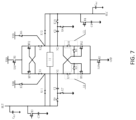
- FIG. 7 is a circuit diagram of a sensitivity amplifier in a write-back state according to an embodiment of the present disclosure.
- the present invention provides a sensitivity amplifier, including: a pre-charge module 11 , a first input and output terminal N 1 , a second input and output terminal N 2 , a first PMOS transistor MP 1 , the second PMOS transistor MP 2 , the first NMOS transistor MN 1 , the second NMOS transistor MN 2 , the first switching unit K 1 , the second switching unit K 2 , the third switching unit 12 , the fourth switching unit 13 , the fifth switching unit K 5 , and the sixth switch unit K 6 , the seventh switch unit K 7 , the eighth switch unit K 8 , the first energy storage unit C 1 and the second energy storage unit C 2 ; wherein, one end of the pre-charge module 11 is connected to the first bit line BLT, and the other end of the pre-charge module 11 is connected to the second bit line BLC.
- the pre-charge module 11 pre-charges the first bit line BLT and the second bit line BLC to a preset voltage; the first input and output terminal N 1 is connected to the first bit line BLT; the second input and output terminal N 2 is connected to the second bit line BLC; the gate of the first PMOS transistor MP 1 is connected to the second input and output terminal N 2 via the second switch unit K 2 , and the drain of the first PMOS transistor MP 1 is connected via the first switch unit K 1 to the first input and output terminal N 1 ; the gate of the second PMOS transistor MP 2 is connected to the first input and output terminal N 1 through the first switch unit K 1 , and the drain of the second PMOS transistor MP 2 is connected to the first input and output terminal N 2 through the second switch unit K 2 .
- the gate of the first NMOS transistor MN 1 is connected to the second input and output terminal N 2 , and is connected to the first input and output terminal N 1 through the third switch unit 12 , and the drain of the first NMOS transistor MN 1 is connected to the first input and output terminal N 1 through the third switch unit 12 ; the gate of the second NMOS transistor MN 2 is connected to the first input and output terminal N 1 , and is connected to the second input and output terminal N 2 through the fourth switch unit 13 .
- the drain of the second NMOS transistor MN 2 is connected to the second input/output terminal N 2 via the fourth switch unit 13 ; one end of the fifth switch unit K 5 is connected to the power supply voltage VDD, and the other end is connected to the first input/output terminal N 1 .
- One end of the sixth switch unit K 6 is connected to the power supply voltage VDD, and the other end is connected to the second input and output terminal N 2 .
- One end of the first energy storage unit C 1 is connected to the first input and output terminal N 1 , and the other end is grounded through the seventh switch unit K 7 .
- One end of the second energy storage unit C 2 is connected to the second input and output terminal N 2 , and the other end is grounded through the eighth switch unit K 8 .
- the first switch unit K 1 , the second switch unit K 2 , the third switch unit 12 , and the fourth switch unit 13 are configured to set the first PMOS transistor MP 1 , the second PMOS transistor MP 2 , the first NMOS transistor MN 1 , and the second NMOS transistor MN 2 into the amplification mode or the diode mode.
- the above-mentioned sensitivity amplifier can compensate for the offset voltage, so that the offset voltage of the sensitivity amplifier is significantly reduced, thereby improving the sensitivity and resolution of the sensitivity amplifier.
- the sensitivity amplifier further includes: a ninth switch unit K 9 and a tenth switch unit K 10 ; one end of the ninth switch unit K 9 is connected to the first bit line BLT, and the other end of the ninth switch unit K 9 is connected to one end of the first energy storage capacitor C 1 ; one end of the tenth switch unit K 10 is connected to the second bit line BLC, and the other end of the tenth switch unit K 10 is connected to one end of the second energy storage capacitor C 2 .
- the sensitivity amplifier further includes: an eleventh switch unit K 11 and a twelfth switch unit K 12 ; one end of the eleventh switch unit K 11 is connected to the first bit line BLT, and the other end of the eleventh switch unit K 11 is connected to the first input/output terminal N 1 ; one end of the twelfth switch unit K 12 is connected to the second bit line BLC, and the other end of the twelfth switch unit K 12 is connected to the second input and output terminal N 2 .
- the first switch unit K 1 , the second switch unit K 2 , the fifth switch unit K 5 , the sixth switch unit K 6 , the seventh switch unit K 7 , the eighth switch unit K 8 , the ninth switch unit K 9 , and the tenth switch unit K 10 , the eleventh switch unit K 11 , and the twelfth switch unit K 12 may all be NMOS transistors or transmission gates composed of NMOS and PMOS transistors.
- the transmission gate refers a bilateral switch consisting of NMOS and PMOS transistors controlled by externally applied logic levels.
- the sensitivity amplifier further includes: a first driving transistor M 1 and a second driving transistor M 2 ; one end of the first driving transistor M 1 is connected to the power supply voltage VDD, and the other end is connected to the source of the first PMOS transistor MP 1 and the source of the second PMOS transistor MP 2 ; one end of the second driving transistor M 2 is grounded, and the other end is connected to the source of the first NMOS transistor MN 1 and the source of the second NMOS transistor MN 2 .
- the first driving transistor M 1 includes a PMOS transistor, the source of the first driving transistor M 1 is connected to the power supply voltage VDD, the drain of the first driving transistor M 1 is connected to the source of the first PMOS transistor MP 1 and the second PMOS transistor MP 2 .
- the source of the second driving transistor M 2 comprises an NMOS transistor, the source of the second driving transistor M 2 is grounded, the drain of the second driving transistor M 2 is connected to the source of the first NMOS transistor MN 1 and the source of the second NMOS transistor MN 2 .
- the sensitivity amplifier further includes a first switch transistor M 3 , a second switch transistor M 4 , a third energy storage unit capacitor C 3 , and a fourth energy storage unit capacitor C 4 ; one end of the first switch transistor M 3 is connected to the first bit line BLT, the other end of the first switch transistor M 3 is connected to one end of the third energy storage unit C 3 , and the other end of the third energy storage unit C 3 is grounded; one end of the second switch transistor M 4 is connected to the second bit line BLC, and the other end of the second switch transistor M 4 is connected to one end of the fourth energy storage unit C 4 , and the other end of the fourth energy storage unit C 4 is grounded.
- the first switching transistor M 3 may be an NMOS transistor, the drain of the first switching transistor M 3 is connected to the first bit line BLT, and the source of the first switching transistor M 3 is connected to the third energy storage unit C 3 ;
- the second switching transistor M 4 may be an NMOS transistor, the drain of the second switching transistor M 4 is connected to the second bit line BLC, and the source of the second switching transistor M 4 is connected to the fourth energy storage unit C 4 .
- the third switch unit 12 includes a third switch transistor K 31 and a fifth switch transistor K 32
- the fourth switch unit 13 includes a fourth switch transistor K 41 and a sixth switch transistor K 42 ; one end of the third switch transistor K 31 is connected to the input and output terminal N 1 , the other end of the third switch transistor K 31 is connected to the drain of the first NMOS transistor MN 1 , one end of the fifth switch transistor K 32 is connected to the drain of the first NMOS transistor MN 1 , and the other end of the fifth switch transistor K 32 is connected to the gate of the first NMOS transistor MN 1 ; one end of the fourth switch transistor K 41 is connected to the second input and output terminal N 2 , the other end of the fourth switch transistor K 41 is connected to the drain of the second NMOS transistor MN 2 , and one end of the sixth switch transistor K 42 is connected to the drain of the second NMOS transistor MN 2 , and the other end of the sixth switch transistor K 42 is connected to the gate of the second NMOS transistor MN 2
- the third switch transistor K 31 , the fourth switch transistor K 41 , the fifth switch transistor K 32 , and the sixth switch transistor K 42 are all NMOS transistors or transmission gates composed NMOS and PMOS transistors.
- the present invention also provides a control method of the above-mentioned sensitivity amplifier, including:
- Pre-charge stage pre-charge the first bit line BLT and the second bit line BLC to preset voltage
- Offset-voltage compensation stage adjust the connection modes of the first PMOS transistor MP 1 , the second PMOS transistor MP 2 , the first NMOS transistor MN 1 and the second NMOS transistor MN 2 , so as to compensate the offset voltage difference of the first input and output terminal N 1 and the second input and output terminal N 2 .
- a pre-charge (EQ) module 11 is used to pre-charge the first bit line BLT and the second bit line BLC to a preset voltage.
- the pre-charge module 11 is disconnected.
- the preset voltage may be half of the power supply voltage or other values.
- the offset-voltage compensation stage includes the following steps: first, the first switch unit K 1 , the second switch unit K 2 , the eleventh switch unit K 11 , the twelfth switch unit K 12 , the third switch unit 12 , and the fourth switch unit 13 are all placed in the open (off) state, and the fifth switch unit K 5 , the sixth switch unit K 6 , the seventh switch unit K 7 , and the eighth switch unit K 8 are placed in the closed (on) state, as shown in FIG. 2 .
- the input and output terminals N 1 and the second input and output terminals N 2 are charged to the power supply voltage VDD; then, the fifth switch unit K 5 and the sixth switch unit K 6 are placed in the of state, and the fifth switch transistor K 32 is closed to turn on the first NMOS transistor MN 1 , where the gate of MN 1 is directly connected with the drain of the first NMOS transistor MN 1 , and the sixth switch transistor K 42 is closed to short connect the gate and the drain of the second NMOS transistor MN 2 , as shown in FIG. 3 .
- the voltage of the first input and output terminal N 1 is discharged to the threshold voltage of the second NMOS transistor MN 2
- the voltage of the second input and output terminal N 2 is discharged to the threshold voltage of the first NMOS transistor MN 1 .
- the charge on the threshold voltage of the first NMOS transistor MN 1 is stored on the second energy storage unit C 2
- the charge on the threshold voltage of the second NMOS transistor MN 2 is stored on the first energy storage unit C 1 .
- the offset-voltage compensation stage is followed with:
- Small signal amplification stage connect the first NMOS transistor MN 1 and the second NMOS transistor MN 2 into an amplification mode, and amplify the voltage difference between the first input and output terminal N 1 and the second input and output terminal N 2 ; connect the first PMOS transistor MP 1 and the second PMOS transistor MP 2 to an amplification mode, and pulled up the voltage of the first input/output terminal N 1 or the voltage of the second input/output terminal N 2 to the power supply voltage VDD.
- the small signal amplification stage includes: first, jump up the voltage of the control terminal of the first switch transistor M 3 from a low to a high level, so that the first switch transistor M 3 is turned on, and the third energy storage unit C 3 is connected to the first bit line BLT. As shown in FIG. 4 , when the voltage of the third energy storage unit C 3 is lower than the voltage of the first bit line BLT, the first bit line BLT charges the third energy storage unit C 3 .
- the third energy storage unit C 3 charges the first bit line BLT; secondly, close the ninth switch unit K 9 and the tenth switch unit K 10 , and disconnect the seventh switch unit K 7 and the eighth switch unit K 8 , the fifth switch transistor K 32 and the sixth switch transistor K 42 , and close the third switch transistor K 31 and the fourth switch transistor K 41 , as shown in FIG. 5 .
- the voltage at the first input and output terminal N 1 is the sum of the threshold voltage of the second NMOS transistor MN 2 and the voltage of the first bit line BLT
- the voltage at the second input and output terminal N 2 is the sum of the threshold voltage of the first NMOS transistor NM 1 and the voltage of the second bit line BLC.
- the first NMOS transistor MN 1 and the second NMOS transistor MN 2 are connected in amplification mode to facilitate the amplification of the differential input signal.
- the first PMOS transistor MP 1 and the second PMOS transistor MP 2 are not involved in the amplification process.
- the third energy storage unit C 3 charges the first bit line BLT in the process of FIG. 4 , the voltage of the first input and output terminal N 1 in the process in FIG. 5 is greater than the voltage of the second input and output terminal N 2 . If the first bit line BLT charges the third energy storage unit C 3 in the process of FIG. 4 , the voltage of the first input and output terminal N 1 in the process of FIG. 5 is less than the voltage of the second input and output terminal N 2 . Finally, the first switch unit K 1 and the second switch unit K 2 are closed to connect the first PMOS transistor MP 1 and the second PMOS transistor MP 2 , as shown in FIG. 6 .
- the voltage SAP of the control terminal of the first drive transistor M 1 is pulled down to turn on the first driving transistor M 1 , the first PMOS transistor MP 1 and the second PMOS transistor MP 2 are connected into the amplification mode.
- the first PMOS transistor MP 1 and the second PMOS transistor MP 2 are used to pull up the first input and output terminal N 1 or the second input and output terminal N 2 to the power supply voltage VDD. Specifically, before the process shown in FIG.
- the first PMOS transistor MP 1 enhances its pull-up
- the first NMOS transistor MN 1 reduces its pull-down
- the voltage of the first input and output terminal N 1 is pulled up to the power supply voltage VDD
- the second PMOS transistor MP 2 reduces its pull-up
- the second NMOS transistor MN 2 enhances its pull-down, so the voltage of the second input and output terminal N 2 is pulled down to the ground voltage (GND).
- GND ground voltage
- the second PMOS transistor MP 2 enhances its pull-up
- the second NMOS transistor MN 2 reduces its pull-down, so the voltage of the second input and output terminal N 2 is pulled up to the power supply voltage VDD.
- the first PMOS transistor MP 1 reduces its pull-up
- the first NMOS transistor MN 1 enhances its pull-down, so the voltage of the first input and output terminal N 1 is pulled down to the ground voltage.
- the voltage of the first input and output terminal N 1 and the voltage of the second input and output terminal N 2 have been differentiated by a larger value, that is, the voltage of the first input and output terminal N 1 and the voltage of the second input and output terminal N 2 are quite different now, thus the mismatch between the first PMOS transistor MP 1 and the second PMOS transistor MP 2 is not enough to induce a reading error.
- the write-back stage includes specifically: place the eleventh switch unit K 11 in a closed state to write back to the first bit line BLT; more specifically: disconnect the ninth switch unit K 9 , and close the eleventh switch unit K 11 , thus the first input and output terminal N 1 charges the third energy storage unit C 3 to facilitate writing back to the first bit line BLT.
Landscapes
- Engineering & Computer Science (AREA)
- Microelectronics & Electronic Packaging (AREA)
- Computer Hardware Design (AREA)
- Dram (AREA)
- Amplifiers (AREA)
Applications Claiming Priority (3)
| Application Number | Priority Date | Filing Date | Title |
|---|---|---|---|
| CN201911188084.5A CN112863561B (zh) | 2019-11-28 | 2019-11-28 | 灵敏放大器及其控制方法 |
| CN201911188084.5 | 2019-11-28 | ||
| PCT/CN2020/097046 WO2021103501A1 (fr) | 2019-11-28 | 2020-06-19 | Amplificateur sensible et son procédé de commande |
Publications (2)
| Publication Number | Publication Date |
|---|---|
| US20220148628A1 US20220148628A1 (en) | 2022-05-12 |
| US11790959B2 true US11790959B2 (en) | 2023-10-17 |
Family
ID=75985246
Family Applications (1)
| Application Number | Title | Priority Date | Filing Date |
|---|---|---|---|
| US17/430,709 Active 2041-03-24 US11790959B2 (en) | 2019-11-28 | 2020-06-19 | Sensitivity amplifier |
Country Status (4)
| Country | Link |
|---|---|
| US (1) | US11790959B2 (fr) |
| EP (1) | EP3920185B1 (fr) |
| CN (1) | CN112863561B (fr) |
| WO (1) | WO2021103501A1 (fr) |
Cited By (1)
| Publication number | Priority date | Publication date | Assignee | Title |
|---|---|---|---|---|
| US20230019429A1 (en) * | 2021-07-16 | 2023-01-19 | Changxin Memory Technologies, Inc. | Receiver, memory and testing method |
Families Citing this family (6)
| Publication number | Priority date | Publication date | Assignee | Title |
|---|---|---|---|---|
| CN112863561B (zh) | 2019-11-28 | 2024-05-03 | 长鑫存储技术有限公司 | 灵敏放大器及其控制方法 |
| CN116168737B (zh) * | 2021-11-24 | 2024-05-14 | 长鑫存储技术有限公司 | 感测放大电路以及数据读出方法 |
| US12112824B2 (en) | 2021-11-24 | 2024-10-08 | Changxin Memory Technologies, Inc. | Sense amplifier circuit and data read method |
| US12100441B2 (en) * | 2022-01-14 | 2024-09-24 | Changxin Memory Technologies, Inc. | Readout circuit layout and sense amplification circuit |
| KR20230167612A (ko) * | 2022-06-02 | 2023-12-11 | 삼성전자주식회사 | 반도체 메모리 장치의 비트라인 센스앰프 및 비트라인 센싱방법 |
| CN117497023B (zh) * | 2023-11-03 | 2024-05-03 | 北京超弦存储器研究院 | 感应放大器及其控制方法、存储阵列结构及存储器 |
Citations (13)
| Publication number | Priority date | Publication date | Assignee | Title |
|---|---|---|---|---|
| US20110292709A1 (en) * | 2010-05-28 | 2011-12-01 | Elpida Memory, Inc. | Semiconductor device |
| US20140204683A1 (en) * | 2013-01-23 | 2014-07-24 | Lsi Corporation | Margin free pvt tolerant fast self-timed sense amplifier reset circuit |
| CN104036821A (zh) * | 2014-06-12 | 2014-09-10 | 江南大学 | 一种改进型交叉耦合灵敏放大器 |
| CN104269189A (zh) | 2014-10-27 | 2015-01-07 | 北海市蕴芯电子科技有限公司 | 一种微功耗eeprom灵敏放大器电路 |
| US20150380079A1 (en) * | 2014-06-27 | 2015-12-31 | International Business Machines Corporation | Low power sense amplifier for static random access memory |
| CN105895139A (zh) | 2016-03-30 | 2016-08-24 | 上海华虹宏力半导体制造有限公司 | 灵敏放大器 |
| US9437282B1 (en) * | 2015-08-06 | 2016-09-06 | Globalfoundries Inc. | High performance sense amplifier |
| CN106205664A (zh) | 2016-06-28 | 2016-12-07 | 醴陵恒茂电子科技有限公司 | 存储器读写传输门管控电路 |
| CN109166598A (zh) | 2018-08-17 | 2019-01-08 | 长鑫存储技术有限公司 | 灵敏放大器电路、存储器及信号放大方法 |
| CN109841240A (zh) * | 2018-12-21 | 2019-06-04 | 北京时代民芯科技有限公司 | 一种sram型存储器高速灵敏放大器电路 |
| US20200194059A1 (en) * | 2018-12-13 | 2020-06-18 | International Business Machines Corporation | Memory array with reduced circuitry |
| US20210043266A1 (en) * | 2016-03-22 | 2021-02-11 | Micron Technology, Inc. | Apparatus and methods for debugging on a host and memory device |
| WO2021103501A1 (fr) | 2019-11-28 | 2021-06-03 | 长鑫存储技术有限公司 | Amplificateur sensible et son procédé de commande |
Family Cites Families (12)
| Publication number | Priority date | Publication date | Assignee | Title |
|---|---|---|---|---|
| US5499218A (en) * | 1995-01-31 | 1996-03-12 | Goldstar Electron Co., Ltd. | Method for driving bit line selecting signals |
| KR20000065800A (ko) * | 1999-04-09 | 2000-11-15 | 윤종용 | 차동 센스증폭기의 오프셋 전압 보상 회로 |
| DE10022263A1 (de) * | 2000-05-08 | 2001-11-22 | Infineon Technologies Ag | Speicher-Leseverstärker |
| US20070024325A1 (en) * | 2005-08-01 | 2007-02-01 | Chung-Kuang Chen | Sense amplifier with input offset compensation |
| US7916556B2 (en) * | 2007-01-09 | 2011-03-29 | Sony Corporation | Semiconductor memory device, sense amplifier circuit and memory cell reading method using a threshold correction circuitry |
| CN101916583B (zh) * | 2010-07-30 | 2015-12-09 | 上海华虹宏力半导体制造有限公司 | 灵敏放大器以及存储器 |
| KR101858579B1 (ko) * | 2011-04-29 | 2018-05-17 | 에스케이하이닉스 주식회사 | 센스 앰프 회로 |
| JP2014102870A (ja) * | 2012-11-21 | 2014-06-05 | Toshiba Corp | センスアンプ回路 |
| KR102319827B1 (ko) * | 2017-06-28 | 2021-11-01 | 에스케이하이닉스 주식회사 | 증폭기 회로 |
| CN108231100B (zh) * | 2018-03-26 | 2023-09-19 | 安徽大学 | 失调电压自适应数字校准型灵敏放大器 |
| CN108648775B (zh) * | 2018-05-07 | 2023-10-20 | 长鑫存储技术有限公司 | 灵敏放大器、半导体存储装置及电压差的放大方法 |
| CN210575115U (zh) * | 2019-11-28 | 2020-05-19 | 长鑫存储技术有限公司 | 灵敏放大器 |
-
2019
- 2019-11-28 CN CN201911188084.5A patent/CN112863561B/zh active Active
-
2020
- 2020-06-19 US US17/430,709 patent/US11790959B2/en active Active
- 2020-06-19 WO PCT/CN2020/097046 patent/WO2021103501A1/fr not_active Ceased
- 2020-06-19 EP EP20893181.6A patent/EP3920185B1/fr active Active
Patent Citations (13)
| Publication number | Priority date | Publication date | Assignee | Title |
|---|---|---|---|---|
| US20110292709A1 (en) * | 2010-05-28 | 2011-12-01 | Elpida Memory, Inc. | Semiconductor device |
| US20140204683A1 (en) * | 2013-01-23 | 2014-07-24 | Lsi Corporation | Margin free pvt tolerant fast self-timed sense amplifier reset circuit |
| CN104036821A (zh) * | 2014-06-12 | 2014-09-10 | 江南大学 | 一种改进型交叉耦合灵敏放大器 |
| US20150380079A1 (en) * | 2014-06-27 | 2015-12-31 | International Business Machines Corporation | Low power sense amplifier for static random access memory |
| CN104269189A (zh) | 2014-10-27 | 2015-01-07 | 北海市蕴芯电子科技有限公司 | 一种微功耗eeprom灵敏放大器电路 |
| US9437282B1 (en) * | 2015-08-06 | 2016-09-06 | Globalfoundries Inc. | High performance sense amplifier |
| US20210043266A1 (en) * | 2016-03-22 | 2021-02-11 | Micron Technology, Inc. | Apparatus and methods for debugging on a host and memory device |
| CN105895139A (zh) | 2016-03-30 | 2016-08-24 | 上海华虹宏力半导体制造有限公司 | 灵敏放大器 |
| CN106205664A (zh) | 2016-06-28 | 2016-12-07 | 醴陵恒茂电子科技有限公司 | 存储器读写传输门管控电路 |
| CN109166598A (zh) | 2018-08-17 | 2019-01-08 | 长鑫存储技术有限公司 | 灵敏放大器电路、存储器及信号放大方法 |
| US20200194059A1 (en) * | 2018-12-13 | 2020-06-18 | International Business Machines Corporation | Memory array with reduced circuitry |
| CN109841240A (zh) * | 2018-12-21 | 2019-06-04 | 北京时代民芯科技有限公司 | 一种sram型存储器高速灵敏放大器电路 |
| WO2021103501A1 (fr) | 2019-11-28 | 2021-06-03 | 长鑫存储技术有限公司 | Amplificateur sensible et son procédé de commande |
Non-Patent Citations (1)
| Title |
|---|
| PCT/CN2020/097046 International Search Report dated Sep. 29, 2020, English translation. |
Cited By (2)
| Publication number | Priority date | Publication date | Assignee | Title |
|---|---|---|---|---|
| US20230019429A1 (en) * | 2021-07-16 | 2023-01-19 | Changxin Memory Technologies, Inc. | Receiver, memory and testing method |
| US12021525B2 (en) * | 2021-07-16 | 2024-06-25 | Changxin Memory Technologies, Inc. | Receiver, memory and testing method |
Also Published As
| Publication number | Publication date |
|---|---|
| CN112863561B (zh) | 2024-05-03 |
| CN112863561A (zh) | 2021-05-28 |
| US20220148628A1 (en) | 2022-05-12 |
| EP3920185A1 (fr) | 2021-12-08 |
| WO2021103501A1 (fr) | 2021-06-03 |
| EP3920185B1 (fr) | 2023-05-31 |
| EP3920185A4 (fr) | 2022-05-25 |
Similar Documents
| Publication | Publication Date | Title |
|---|---|---|
| US11790959B2 (en) | Sensitivity amplifier | |
| CN210575115U (zh) | 灵敏放大器 | |
| US8953400B2 (en) | Data control circuit | |
| KR20100097891A (ko) | 비휘발성 메모리 장치 및 이를 위한 바이어스 생성 회로 | |
| US8125840B2 (en) | Reference level generation with offset compensation for sense amplifier | |
| US20090146697A1 (en) | Circuit for buffering having a coupler | |
| US7795905B2 (en) | On die termination (ODT) circuit having improved high frequency performance | |
| US7088628B2 (en) | Memory device and method of amplifying voltage levels of bit line and complementary bit line | |
| KR100925368B1 (ko) | 센스앰프 전압 공급 회로 및 그의 구동 방법 | |
| CN106205664B (zh) | 存储器读写传输门管控电路 | |
| US6456120B1 (en) | Capacitor-coupling differential logic circuit | |
| US8238137B2 (en) | Ferroelectric random access memory device | |
| US8861291B2 (en) | Memory apparatus and signal delay circuit for generating delayed column select signal | |
| US10726900B2 (en) | Semiconductor memory device and method for reading semiconductor memory device | |
| US8995219B2 (en) | Word line driver | |
| CN108806744B (zh) | 一种延时产生电路及非易失性存储器读时序产生电路 | |
| US11705898B2 (en) | Off chip driver circuit, off chip driver system, and method for manufacturing an off chip driver circuit | |
| US8842489B2 (en) | Fast-switching word line driver | |
| KR100463816B1 (ko) | 충전회로 및 이를 이용한 반도체기억장치 | |
| US20040196716A1 (en) | Semiconductor memory device | |
| US7027340B2 (en) | Output device for static random access memory | |
| US9093130B2 (en) | Sense amplifier with shielding circuit | |
| CN111596866B (zh) | 长线驱动电路以及方法、电子设备 | |
| US7126379B2 (en) | Output device for static random access memory | |
| US20100302892A1 (en) | Semiconductor memory device and method of driving the same |
Legal Events
| Date | Code | Title | Description |
|---|---|---|---|
| FEPP | Fee payment procedure |
Free format text: ENTITY STATUS SET TO UNDISCOUNTED (ORIGINAL EVENT CODE: BIG.); ENTITY STATUS OF PATENT OWNER: LARGE ENTITY |
|
| STPP | Information on status: patent application and granting procedure in general |
Free format text: DOCKETED NEW CASE - READY FOR EXAMINATION |
|
| AS | Assignment |
Owner name: CHANGXIN MEMORY TECHNOLOGIES, INC., CHINA Free format text: ASSIGNMENT OF ASSIGNORS INTEREST;ASSIGNOR:JI, RUMIN;REEL/FRAME:059842/0033 Effective date: 20210727 |
|
| STPP | Information on status: patent application and granting procedure in general |
Free format text: NOTICE OF ALLOWANCE MAILED -- APPLICATION RECEIVED IN OFFICE OF PUBLICATIONS |
|
| STPP | Information on status: patent application and granting procedure in general |
Free format text: PUBLICATIONS -- ISSUE FEE PAYMENT RECEIVED |
|
| STPP | Information on status: patent application and granting procedure in general |
Free format text: PUBLICATIONS -- ISSUE FEE PAYMENT VERIFIED |
|
| STCF | Information on status: patent grant |
Free format text: PATENTED CASE |