US12164852B2 - Layout method and layout apparatus for integrated circuit - Google Patents
Layout method and layout apparatus for integrated circuit Download PDFInfo
- Publication number
- US12164852B2 US12164852B2 US17/504,734 US202117504734A US12164852B2 US 12164852 B2 US12164852 B2 US 12164852B2 US 202117504734 A US202117504734 A US 202117504734A US 12164852 B2 US12164852 B2 US 12164852B2
- Authority
- US
- United States
- Prior art keywords
- pattern
- region
- width
- element region
- filling
- Prior art date
- Legal status (The legal status is an assumption and is not a legal conclusion. Google has not performed a legal analysis and makes no representation as to the accuracy of the status listed.)
- Active, expires
Links
Images


Classifications
-
- G—PHYSICS
- G06—COMPUTING OR CALCULATING; COUNTING
- G06F—ELECTRIC DIGITAL DATA PROCESSING
- G06F30/00—Computer-aided design [CAD]
- G06F30/30—Circuit design
- G06F30/39—Circuit design at the physical level
- G06F30/392—Floor-planning or layout, e.g. partitioning or placement
-
- G—PHYSICS
- G06—COMPUTING OR CALCULATING; COUNTING
- G06F—ELECTRIC DIGITAL DATA PROCESSING
- G06F30/00—Computer-aided design [CAD]
- G06F30/30—Circuit design
- G06F30/39—Circuit design at the physical level
- G06F30/398—Design verification or optimisation, e.g. using design rule check [DRC], layout versus schematics [LVS] or finite element methods [FEM]
-
- H—ELECTRICITY
- H10—SEMICONDUCTOR DEVICES; ELECTRIC SOLID-STATE DEVICES NOT OTHERWISE PROVIDED FOR
- H10B—ELECTRONIC MEMORY DEVICES
- H10B12/00—Dynamic random access memory [DRAM] devices
-
- H—ELECTRICITY
- H10—SEMICONDUCTOR DEVICES; ELECTRIC SOLID-STATE DEVICES NOT OTHERWISE PROVIDED FOR
- H10B—ELECTRONIC MEMORY DEVICES
- H10B12/00—Dynamic random access memory [DRAM] devices
- H10B12/01—Manufacture or treatment
- H10B12/02—Manufacture or treatment for one transistor one-capacitor [1T-1C] memory cells
-
- H—ELECTRICITY
- H10—SEMICONDUCTOR DEVICES; ELECTRIC SOLID-STATE DEVICES NOT OTHERWISE PROVIDED FOR
- H10D—INORGANIC ELECTRIC SEMICONDUCTOR DEVICES
- H10D89/00—Aspects of integrated devices not covered by groups H10D84/00 - H10D88/00
-
- H—ELECTRICITY
- H10—SEMICONDUCTOR DEVICES; ELECTRIC SOLID-STATE DEVICES NOT OTHERWISE PROVIDED FOR
- H10D—INORGANIC ELECTRIC SEMICONDUCTOR DEVICES
- H10D89/00—Aspects of integrated devices not covered by groups H10D84/00 - H10D88/00
- H10D89/10—Integrated device layouts
-
- G—PHYSICS
- G06—COMPUTING OR CALCULATING; COUNTING
- G06F—ELECTRIC DIGITAL DATA PROCESSING
- G06F2117/00—Details relating to the type or aim of the circuit design
- G06F2117/12—Sizing, e.g. of transistors or gates
-
- G—PHYSICS
- G06—COMPUTING OR CALCULATING; COUNTING
- G06F—ELECTRIC DIGITAL DATA PROCESSING
- G06F2119/00—Details relating to the type or aim of the analysis or the optimisation
- G06F2119/18—Manufacturability analysis or optimisation for manufacturability
Definitions
- the present application relates to the field of integrated circuit manufacturing, and in particular, to a layout method and a layout apparatus for an integrated circuit.
- a Dynamic Random Access Memory is a semiconductor device commonly used in electronic devices such as computers, and consists of a plurality of repeating memory cells. Each memory cell generally includes a transistor and a capacitor.
- the transistor has a gate electrically connected to a wordline, a source electrically connected to a bitline and a drain electrically connected to the capacitor.
- a wordline voltage on the wordline can control ON and OFF of the transistor so that through the bitline, data information stored in the capacitor can be read or data information is written to the capacitor.
- a process library has three small trench lengths (5X m, 6X nm, and 7X nm).
- the smaller size makes a single-node process of the DRAM more complex, and an etch error is very easy to occur in a manufacturing process.
- pseudo-gates with a corresponding length and spaced by a specific distance may generally be added to two sides of the transistor to facilitate the formation of diffraction during photolithography, so as to improve the etch accuracy of the trench length of the transistor in an edge region.
- Embodiments of the present application provide a layout method and a layout apparatus for an integrated circuit, which solves the problem of low efficiency of an existing integrated circuit layout to some extent, so as to improve the layout precision, improve the photolithography quality, shorten the development cycle of the integrated circuit, and improve the yield of semiconductor products.
- a layout method for an integrated circuit including the following steps:
- a layout apparatus for an integrated circuit including:
- a width of a spacing region between two adjacent element regions in a layout is automatically detected, and an element region and/or a spacing region not meeting a filling requirement of a dummy pattern are/is marked, so as to quickly and accurately position a poorly-placed element region in the layout, so that the layout can be adjusted in time, which saves human resources, improves the layout efficiency and layout precision of the integrated circuit, and lays a foundation for improving the photolithography quality, shortening the development cycle of the integrated circuit, and improving the yield of semiconductor products and the like.
- FIG. 1 is a flowchart of a layout method for an integrated circuit according to a specific implementation of the present application
- FIG. 2 A to FIG. 2 D are schematic diagrams of detection of a layout according to a specific implementation of the present application
- FIG. 3 A to FIG. 3 J are schematic diagrams of filling of layouts under different scenarios with dummy patterns according to a specific implementation of the present application.
- FIG. 4 is a structural block diagram of a layout apparatus for an integrated circuit according to a specific implementation of the present application.
- FIG. 1 is a flowchart of a layout method for an integrated circuit according to a specific implementation of the present application
- FIG. 2 A to FIG. 2 D are schematic diagrams of detection of a layout according to a specific implementation of the present application.
- the layout method for an integrated circuit according to the specific implementation includes the following steps.
- step S 11 a layout is provided, the layout including a first element region 21 and a second element region 22 , a spacing region 23 being provided between the first element region 21 and the second element region 22 , as shown in FIG. 2 A .
- the layout includes a plurality of element regions that may be arranged according to a layout requirement of the integrated circuit.
- Each element region includes a plurality of elements. Structures and arrangement manners of the elements in each element region may be the same or different, and a spacing region is provided between the adjacent element regions. The spacing region is configured to be filled with a dummy pattern to meet diffraction requirements during subsequent photolithography of the element region.
- the element may be, but is not limited to, a transistor.
- step S 12 it is detected whether a width D of the spacing region 23 is less than a preset width, and if yes, at least one of the first element region 21 , the second element region 22 and the spacing region 23 is marked, and the preset width is a minimum width meeting a requirement, wherein the requirement is to fill the spacing region 23 with at least one dummy pattern 24 , as shown in FIG. 2 D .
- the dummy pattern refers to a pattern during photolithography that can not only compensate for the etch accuracy of the element within the element region, but also conform to DRC (Design Rule Verification).
- the preset width refers to a minimum width meeting the requirement of filling the spacing region with at least one dummy pattern, so that the etch accuracy of the element within the element region is improved.
- a space between the first element region 21 and the second element region 22 adjacent to each other is filled with the dummy pattern 24 , which can help the elements within the first element region 21 and/or the second element region 22 better form diffraction in the photolithography, thereby improving the etch accuracy.
- the width D of the spacing region 23 between the first element region 21 and the second element region 22 adjacent to each other in the layout can be automatically detected and marks are made in the layout according to a detection result, so that a layout engineer can quickly and accurately position an unreasonably designed region in the layout, so as to adjust the layout in time and improve a development cycle of the layout.
- Those skilled in the art can set a specific marking manner according to an actual requirement.
- the first element region 21 and the second element region 22 that are unreasonably designed are simultaneously marked with a dashed box as shown in FIG. 2 B .
- Those skilled in the art can also make marks with other patterns, colors or text.
- the first element region 21 includes a first active area 211 , a first gate pattern 212 located in the first active area 211 and a first auxiliary pattern 213 located on one side of the first element region 21 toward the second element region 22
- the second element region 22 includes a second active area 221 , a second gate pattern 222 located in the second active area 221 and a second auxiliary pattern 223 located on one side of the second element region 22 toward the first element region 21
- the step of detecting whether a width D of the spacing region 23 is less than a preset width specifically includes:
- the first element region 21 includes the first active area 211 , and two outer sides of the first active area 211 along an X-axis direction are provided with one first auxiliary pattern 213 respectively.
- the first gate pattern 212 and the first auxiliary pattern 213 extend along a Y-axis direction perpendicular to the X-axis direction, and the first gate pattern 212 and the first auxiliary pattern 213 are arranged along the X-axis direction.
- the first gate pattern 212 may be in a shape (including a line width and a length along the Y-axis direction) the same as the first auxiliary pattern 213 .
- the first auxiliary pattern 213 is configured to help better diffraction formation during the photolithography of the first gate pattern, so as to effectively control a line width of the first gate pattern to be formed (i.e., a width of the first gate pattern along the X-axis direction).
- the second element region 22 includes a second active area 221 , and two outer sides of the second active area 221 along the X-axis direction are provided with one second auxiliary pattern 223 respectively.
- the second gate pattern 222 and the second auxiliary pattern 223 extend along the Y-axis direction perpendicular to the X-axis direction, and the second gate pattern 222 and the second auxiliary pattern 223 are arranged along the X-axis direction.
- the preset width includes a first subpreset width and a second subpreset width
- the first subpreset width is a minimum width simultaneously meeting etch accuracy requirements of the first auxiliary pattern 213 and the dummy pattern 24
- the second subpreset width is a minimum width simultaneously meeting etch accuracy requirements of the second auxiliary pattern 223 and the dummy pattern.
- Specific values of the first subpreset width and the second subpreset width may be determined according to the etch accuracy that can be achieved by an etchtool actually used. Ranges of the first subpreset width and the second subpreset width are limited, so as to ensure that the dummy pattern 24 for filling can simultaneously meet etch requirements of the first element region 21 and the second element region 22 .
- the method further includes the following step:
- the width of the spacing region 23 may be adjusted in any one of the following three manners: translating the first element region 21 in a direction along the X-axis and away from the second element region 22 ; or translating the second element region 22 in a direction along the X-axis and away from the first element region 21 ; or simultaneously moving the first element region 21 and the second element region 22 in a direction along the X-axis and facing away from each other (as shown in FIG. 2 C ), so that the spacing region 23 can be filled with at least one dummy pattern 24 .
- the layout method for an integrated circuit further includes the following step:
- the spacing region 23 is filled with at least one dummy pattern 24 .
- An example in which the spacing region 23 can be filled with two dummy patterns 24 after the width D of the spacing region 23 is increased to the preset width is described in FIG. 2 D .
- a specific number and shape of the dummy pattern 24 for filling, a distance between the dummy pattern 24 for filling and the first element region 21 as well as a distance between the dummy pattern 24 for filling and the second element region 22 , and distances between adjacent dummy patterns 24 during filling of a plurality of dummy patterns 24 may be set by those skilled in the art according to an actual requirement, for example, according to a line width of the first gate pattern 212 , a line width of the second gate pattern 222 , and the like.
- the step of filling the spacing region 23 with at least one dummy pattern 24 specifically includes:
- the line width W 1 of the first gate pattern 212 and the line width W 2 of the second gate pattern 222 are equal (i.e., the first auxiliary pattern 213 and the second auxiliary pattern 223 are in a same shape) and are both less than a preset size.
- the width D of the spacing region 23 is greater than or equal to the preset width, the spacing region 23 may be filled with one or more dummy patterns 24 .
- An example of filling of one dummy pattern 24 is described in FIG. 3 B . In this case, the shape and size of the dummy pattern 24 for filling are the same as those of the first gate pattern 212 or the second gate pattern 222 .
- a distance between the dummy pattern 24 for filling and the first auxiliary pattern 213 and a distance between the dummy pattern 24 for filling and the second auxiliary pattern 223 are equal.
- the preset size is 10 nm.
- the line width W 1 of the first gate pattern 212 and the line width W 2 of the second gate pattern 222 may be 5 nm, 6 nm or 7 nm.
- the step of filling the spacing region 23 with the at least one dummy pattern 24 specifically includes:
- Whether the width of the spacing region 23 meets a requirement of simultaneous filling of a first dummy pattern 241 and a second dummy pattern 242 specifically includes: a distance between the first dummy pattern 241 filling the spacing region 23 and the first auxiliary pattern 213 being greater than or equal to the first subpreset width, and a distance between the second dummy pattern 242 filling the spacing region 23 and the second auxiliary pattern 223 being greater than or equal to the second subpreset width.
- the line width W 1 of the first gate pattern 212 and the line width W 2 of the second gate pattern 222 are less than the preset size
- the line width W 1 of the first gate pattern 212 is less than the line width W 2 of the second gate pattern 222 (i.e., the line width of the first auxiliary pattern 213 is less than that of the second auxiliary pattern 223 )
- the width of the spacing region 23 meets the requirement of simultaneous filling of the first dummy pattern 241 and the second dummy pattern 242 ; then, the spacing region 23 may be simultaneously filled with two first dummy patterns 241 and two second dummy patterns 242 , as shown in FIG. 3 D .
- the first dummy pattern 241 is located on one side of the spacing region 23 close to the first auxiliary pattern 213 , and a line width of the first dummy pattern 241 is equal to that of the first gate pattern 212 ; the second dummy pattern 242 is located on one side of the spacing region 23 close to the second auxiliary pattern 223 , and a line width of the second dummy pattern 242 is equal to that of the second gate pattern 222 .
- the reason why the spacing region 23 is filled with the two first dummy patterns 241 is that at least three patterns in a same shape (the first auxiliary pattern 213 and the first dummy pattern 241 ) are arranged on one side of the first gate pattern 212 to better improve a diffraction effect of the first gate pattern 212 during photolithography.
- the reason why the spacing region 23 is filled with the two second dummy patterns 242 is that at least three patterns in a same shape (the second auxiliary pattern 223 and the second dummy pattern 242 ) are arranged on one side of the second gate pattern 222 to better improve a diffraction effect of the second gate pattern 222 during photolithography.
- a length of the first dummy pattern 241 for filling (a length along the Y-axis direction in FIG. 3 C ) is equal to a length of the first auxiliary pattern 213 (a length along the Y-axis direction in FIG. 3 C ); and a length of the second dummy pattern 242 for filling (a length along the Y-axis direction in FIG. 3 C ) is equal to a length of the second auxiliary pattern 223 (a length along the Y-axis direction in FIG. 3 C ).
- a distance between the first dummy pattern 241 and the second dummy pattern 242 adjacent to each other and filling the spacing region 23 is greater than or equal to a first threshold.
- a specific value of the first threshold may be set according to process capability and an actual manufacturing condition, such as a photolithography accuracy requirement.
- the method further includes the following step:
- the step of filling the spacing region 23 with at least one dummy pattern 24 specifically includes:
- a length of the first dummy pattern 241 is equal to that of the first auxiliary pattern 213
- a length of the second dummy pattern 242 is equal to that of the second auxiliary pattern 223 .
- the layout method for an integrated circuit further includes the following step:
- the line width W 1 of the first gate pattern 212 is less than the preset size, and the line width W 2 of the second gate pattern 222 is greater than the preset size; that is, the line width W 1 of the first gate pattern 212 is not equal to the line width W 2 of the second gate pattern 222 .
- the spacing region may be filled with only one first dummy pattern 241 having a line width the same as the first gate pattern 212 or the first auxiliary pattern 213 , as shown in FIG. 3 F .
- the spacing region 23 may be filled with only the second dummy pattern 242 .
- a specific value of the first threshold may be set according to process capability and an actual manufacturing condition, such as a photolithography accuracy requirement.
- the first dummy pattern 241 for filling is enabled to be directly connected to the second auxiliary pattern 223 .
- the first dummy pattern 241 for filling is enabled to be isolated from the second auxiliary pattern 223 .
- the layout method for an integrated circuit further includes the following step:
- the space between the first element region 21 and the conductive plug 25 may also be filled with at least two plug dummy patterns 244 , as shown in FIG. 3 H , so that one side of the first gate pattern toward the conductive plug 25 meets the requirement of having at least three patterns in a same shape (including the first auxiliary pattern and the dummy pattern for filling), so as to improve a photolithography effect.
- the line width of the plug dummy pattern 244 is equal to that of the first gate pattern 212
- the length of the dummy pattern 24 is equal to that of the first auxiliary pattern 213 .
- the layout further includes a conductive plug 25 and a third element region 26 adjacent to the first element region 21 ; the third element region 26 includes a third active area, a third gate pattern 261 located in the third active area and a third auxiliary pattern 262 located on an outer side of the third active area; and the layout method for an integrated circuit further includes the following step:
- the blank region 28 in this specific implementation is the region provided with no gate pattern.
- the third dummy pattern 243 matching both the first element region 21 and the third element region 26 means that a shape of the third dummy pattern 243 matches one or more of extension directions, extension lengths and line widths of elements in the first element region 21 and the third element region 26 and a spacing distance between adjacent elements, so as to improve the photolithography quality of the patterns in the first element region 21 and the third element region 26 .
- the first gate pattern 212 and the third gate pattern 261 extend along a first direction, the first gate pattern 212 and the third gate pattern 261 are spaced along a second direction, the first direction is perpendicular to the second direction, and a length or position of the first gate pattern 212 in the first direction is beyond that of the third gate pattern 261 ; and the step of filling the blank region 28 with the third dummy pattern 243 matching both the first element region 21 and the third element region 26 specifically includes:
- the first direction is a Y-axis direction
- the second direction is an X-axis direction.
- the blank region 28 is filled with a plurality of third dummy patterns 243 extending along the Y-axis direction and arranged along the X-axis direction. A boundary of each of the dummy patterns close to one side of the conductive plug 25 is flush with the first gate pattern 212 .
- the plurality of third dummy patterns 243 are aligned with a plurality of third gate patterns 261 in the third element region 26 and the third auxiliary pattern 262 located outside the third active area.
- the blank region 28 is filled with the plurality of third dummy patterns 243 ;
- the blank region 28 may be filled with a plurality of third dummy patterns 243 completely.
- a number of the third dummy pattern 243 filling the blank region 28 is equal to a sum of numbers of the third gate pattern 261 and the third auxiliary pattern 262 in the third element region 26
- the distance between adjacent third dummy patterns 243 is equal to that between the third gate pattern 261 and the third auxiliary pattern 262 .
- the layout method for an integrated circuit further includes the following step:
- the third dummy pattern 243 is set to avoid the metal connection structure 263 , as shown in FIG. 3 J .
- the layout further includes a fourth element region 27 and the first element region 21 , the third element region 26 , the fourth element region 27 and the conductive plug 25 jointly define a blank region, the third dummy pattern for filling should be further aligned with a fourth gate pattern and a fourth auxiliary pattern in the fourth element region.
- a specific value of the second threshold may be set according to process capability and an actual manufacturing condition, such as a photolithography accuracy requirement.
- the first threshold may be equal or not equal to the second threshold, which may be set by those skilled in the art according to an actual manufacturing requirement.
- the method further includes the following step:
- the method further includes the following step:
- the method may further include the following step: determining whether the width of the spacing region 23 is less than the first subpreset width, and if no, filling the spacing region 23 with the first dummy pattern 241 , the first dummy pattern 241 being a pattern with a line width the same as that of the first gate pattern 212 .
- the method may further include the following step: determining whether the width of the spacing region 23 is less than the second subpreset width, and if no, filling the spacing region 23 with the second dummy pattern 242 , the second dummy pattern 242 being a pattern with a line width the same as that of the second gate pattern 222 . That is, a corresponding determination manner can be selected according to relative sizes of the first subpreset width and the second subpreset width.
- the width of the spacing region 23 is determined to be less than the preset width and greater than the first subpreset width, it is determined whether a distance between the first dummy pattern 241 filling the spacing region 23 and the second auxiliary pattern 213 is less than the first threshold, and if yes, the first dummy pattern 241 for filling is enabled to be connected to the second auxiliary pattern 223 .
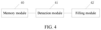
- FIG. 4 is a structural block diagram of a layout apparatus for an integrated circuit according to a specific implementation of the present application.
- the layout apparatus for an integrated circuit according to this specific implementation may lay out a layout by using the layout method for an integrated circuit shown in FIG. 1 , FIG. 2 A to FIG. 2 D and FIG. 3 A to FIG. 3 J .
- the layout apparatus for an integrated circuit according to the specific implementation includes:
- the first element region 21 includes a first active area 211 , a first gate pattern 212 located in the first active area 211 and a first auxiliary pattern 213 located on one side of the first element region 211 toward the second element region 22
- the second element region 22 includes a second active area 221 , a second gate pattern 222 located in the second active area 221 and a second auxiliary pattern 223 located on one side of the second active area 221 toward the first element region 21 ;
- the layout apparatus for an integrated circuit further includes:
- the filling module 42 is further configured to determine whether a line width W 1 of the first gate pattern 212 is equal to a line width W 2 of the second gate pattern 222 , and if yes, fill the spacing region 23 with the at least one dummy pattern 24 , a line width of the dummy pattern 24 being equal to the line width of the first gate pattern 212 or the line width of the second gate pattern 222 .
- the filling module 42 is further configured to determine whether a line width of the first gate pattern 212 is equal to that of the second gate pattern 222 , if no, determine whether the width of the spacing region 23 meets a requirement of simultaneous filling of a first dummy pattern 241 and a second dummy pattern 242 , and if yes, simultaneously fill the spacing region 23 with the first dummy pattern 241 and the second dummy pattern 242 , the first dummy pattern 241 being a pattern with a line width the same as the first gate pattern 212 , and the second dummy pattern 242 being a pattern with a line width the same as the second gate pattern 222 .
- the filling module 42 is further configured to determine whether a line width of the first gate pattern 212 is equal to that of the second gate pattern 222 , if no, determine whether the width of the spacing region 23 meets a requirement of simultaneous filling of a first dummy pattern 241 and a second dummy pattern 242 , if no, re-determine whether the line width of the first gate pattern 212 is less than that of the second gate pattern 222 , if yes, fill the spacing region 23 with only the first dummy pattern 241 , and if no, fill the spacing region 23 with only the second dummy pattern 242 , the first dummy pattern 241 being a pattern with a line width the same as the first gate pattern 212 , and the second dummy pattern 242 being a pattern with a line width the same as the second gate pattern 222 .
- the filling module 42 is further configured to determine whether a conductive plug 25 adjacent to the first element region exists on a periphery of the first element region 21 , and if yes, fill a space between the first element region 21 and the conductive plug 25 with a plug dummy pattern 244 , a line width of the plug dummy pattern 244 being equal to that of the first gate pattern 212 .
- the layout further includes a conductive plug 25 and a third element region 26 adjacent to the first element region 21 ;
- the third element region includes a third active area, a third gate pattern 261 located in the third active area and a third auxiliary pattern 262 located on an outer side of the third active area;
- the detection module 41 is further configured to, after at least one of the first element region 21 , the second element region 22 and the spacing region 23 is marked, adjust positions of the first element region 21 and/or the second element region 22 to increase the width of the spacing region 23 to the preset width.
- a width of a spacing region between two adjacent element regions in a layout is automatically detected, and an element region and/or a spacing region not meeting a filling requirement of a dummy pattern are/is marked, so as to quickly and accurately position a poorly-placed element region in the layout, so that the layout can be adjusted in time, which saves human resources, improves the layout efficiency and layout precision of the integrated circuit, and lays a foundation for improving photolithography quality, shortening a development cycle of the integrated circuit, improving a yield of semiconductor products and the like.
Landscapes
- Engineering & Computer Science (AREA)
- Computer Hardware Design (AREA)
- Physics & Mathematics (AREA)
- Theoretical Computer Science (AREA)
- General Engineering & Computer Science (AREA)
- Evolutionary Computation (AREA)
- Geometry (AREA)
- General Physics & Mathematics (AREA)
- Architecture (AREA)
- Manufacturing & Machinery (AREA)
- Design And Manufacture Of Integrated Circuits (AREA)
Applications Claiming Priority (3)
| Application Number | Priority Date | Filing Date | Title |
|---|---|---|---|
| CN202011237506.6A CN114464613B (zh) | 2020-11-09 | 2020-11-09 | 集成电路的布图方法及布图装置 |
| CN202011237506.6 | 2020-11-09 | ||
| PCT/CN2021/104007 WO2022095485A1 (zh) | 2020-11-09 | 2021-07-01 | 集成电路的布图方法及布图装置 |
Related Parent Applications (1)
| Application Number | Title | Priority Date | Filing Date |
|---|---|---|---|
| PCT/CN2021/104007 Continuation WO2022095485A1 (zh) | 2020-11-09 | 2021-07-01 | 集成电路的布图方法及布图装置 |
Publications (2)
| Publication Number | Publication Date |
|---|---|
| US20220147686A1 US20220147686A1 (en) | 2022-05-12 |
| US12164852B2 true US12164852B2 (en) | 2024-12-10 |
Family
ID=81455338
Family Applications (1)
| Application Number | Title | Priority Date | Filing Date |
|---|---|---|---|
| US17/504,734 Active 2042-11-28 US12164852B2 (en) | 2020-11-09 | 2021-10-19 | Layout method and layout apparatus for integrated circuit |
Country Status (4)
| Country | Link |
|---|---|
| US (1) | US12164852B2 (de) |
| EP (1) | EP4184377A4 (de) |
| JP (1) | JP7450109B2 (de) |
| KR (1) | KR102934464B1 (de) |
Families Citing this family (2)
| Publication number | Priority date | Publication date | Assignee | Title |
|---|---|---|---|---|
| US12547812B2 (en) | 2022-05-25 | 2026-02-10 | Changxin Memory Technologies, Inc. | Method and apparatus for checking signal line |
| CN119556521B (zh) * | 2025-02-05 | 2025-04-25 | 合肥晶合集成电路股份有限公司 | 一种光学临近校正方法 |
Citations (14)
| Publication number | Priority date | Publication date | Assignee | Title |
|---|---|---|---|---|
| US20020087942A1 (en) | 2000-12-28 | 2002-07-04 | Mitsubishi Denki Kabushiki Kaisha | Apparatus for layout designing of semiconductor device, method of layout designing, and semiconductor device |
| US20050193364A1 (en) * | 2001-06-29 | 2005-09-01 | Kabushiki Kaisha Toshiba | Pattern forming method and semiconductor device manufactured by using said pattern forming method |
| US20070168898A1 (en) * | 2006-01-14 | 2007-07-19 | Blaze Dfm, Inc. | Method and system for detailed placement of layout objects in a standard-cell layout design |
| CN101123203A (zh) | 2006-08-11 | 2008-02-13 | 东部高科股份有限公司 | 形成虚拟图形的方法 |
| JP2008122948A (ja) | 2006-10-20 | 2008-05-29 | Toshiba Corp | 設計レイアウト作成方法、半導体装置の製造方法、及びコンピュータ読み取り可能な媒体 |
| CN101364595A (zh) | 2007-08-10 | 2009-02-11 | 东部高科股份有限公司 | 半导体器件布局及在其中放置虚置图案的方法 |
| CN101752368A (zh) | 2008-12-18 | 2010-06-23 | 台湾积体电路制造股份有限公司 | 具有可变设计规则的标准单元架构和方法 |
| CN101819947A (zh) | 2009-02-27 | 2010-09-01 | 台湾积体电路制造股份有限公司 | 形成集成电路结构的方法 |
| US20110029936A1 (en) | 2009-07-30 | 2011-02-03 | Samsung Electronics Co., Ltd. | Method of generating layout of semiconductor device |
| US20130244144A1 (en) * | 2010-10-29 | 2013-09-19 | Texas Instruments Incorporated | Gate cd control using local design on both sides of neighboring dummy gate level features |
| CN103778273A (zh) | 2012-10-23 | 2014-05-07 | Arm有限公司 | 产生包含标准单元及存储器实例的集成电路布图的方法 |
| CN106449628A (zh) | 2015-08-05 | 2017-02-22 | 联华电子股份有限公司 | 半导体布局结构及其设计方法 |
| US20170062582A1 (en) | 2013-12-29 | 2017-03-02 | Texas Instruments Incorporated | Dummy gate placement methodology to enhance integrated circuit performance |
| CN110852032A (zh) | 2018-07-31 | 2020-02-28 | 台湾积体电路制造股份有限公司 | 产生集成电路元件的布局图的方法 |
Family Cites Families (3)
| Publication number | Priority date | Publication date | Assignee | Title |
|---|---|---|---|---|
| JP4488727B2 (ja) * | 2003-12-17 | 2010-06-23 | 株式会社東芝 | 設計レイアウト作成方法、設計レイアウト作成システム、マスクの製造方法、半導体装置の製造方法、及び設計レイアウト作成プログラム |
| JP5262065B2 (ja) * | 2007-10-31 | 2013-08-14 | 富士通株式会社 | レイアウト設計プログラム、該プログラムを記録した記録媒体、レイアウト設計装置、およびレイアウト設計方法 |
| CN103049588B (zh) * | 2011-10-14 | 2016-04-13 | 上海华虹宏力半导体制造有限公司 | 冗余图形的填充方法 |
-
2021
- 2021-07-01 EP EP21888187.8A patent/EP4184377A4/de active Pending
- 2021-07-01 JP JP2023501319A patent/JP7450109B2/ja active Active
- 2021-07-01 KR KR1020237003859A patent/KR102934464B1/ko active Active
- 2021-10-19 US US17/504,734 patent/US12164852B2/en active Active
Patent Citations (14)
| Publication number | Priority date | Publication date | Assignee | Title |
|---|---|---|---|---|
| US20020087942A1 (en) | 2000-12-28 | 2002-07-04 | Mitsubishi Denki Kabushiki Kaisha | Apparatus for layout designing of semiconductor device, method of layout designing, and semiconductor device |
| US20050193364A1 (en) * | 2001-06-29 | 2005-09-01 | Kabushiki Kaisha Toshiba | Pattern forming method and semiconductor device manufactured by using said pattern forming method |
| US20070168898A1 (en) * | 2006-01-14 | 2007-07-19 | Blaze Dfm, Inc. | Method and system for detailed placement of layout objects in a standard-cell layout design |
| CN101123203A (zh) | 2006-08-11 | 2008-02-13 | 东部高科股份有限公司 | 形成虚拟图形的方法 |
| JP2008122948A (ja) | 2006-10-20 | 2008-05-29 | Toshiba Corp | 設計レイアウト作成方法、半導体装置の製造方法、及びコンピュータ読み取り可能な媒体 |
| CN101364595A (zh) | 2007-08-10 | 2009-02-11 | 东部高科股份有限公司 | 半导体器件布局及在其中放置虚置图案的方法 |
| CN101752368A (zh) | 2008-12-18 | 2010-06-23 | 台湾积体电路制造股份有限公司 | 具有可变设计规则的标准单元架构和方法 |
| CN101819947A (zh) | 2009-02-27 | 2010-09-01 | 台湾积体电路制造股份有限公司 | 形成集成电路结构的方法 |
| US20110029936A1 (en) | 2009-07-30 | 2011-02-03 | Samsung Electronics Co., Ltd. | Method of generating layout of semiconductor device |
| US20130244144A1 (en) * | 2010-10-29 | 2013-09-19 | Texas Instruments Incorporated | Gate cd control using local design on both sides of neighboring dummy gate level features |
| CN103778273A (zh) | 2012-10-23 | 2014-05-07 | Arm有限公司 | 产生包含标准单元及存储器实例的集成电路布图的方法 |
| US20170062582A1 (en) | 2013-12-29 | 2017-03-02 | Texas Instruments Incorporated | Dummy gate placement methodology to enhance integrated circuit performance |
| CN106449628A (zh) | 2015-08-05 | 2017-02-22 | 联华电子股份有限公司 | 半导体布局结构及其设计方法 |
| CN110852032A (zh) | 2018-07-31 | 2020-02-28 | 台湾积体电路制造股份有限公司 | 产生集成电路元件的布局图的方法 |
Non-Patent Citations (4)
| Title |
|---|
| Extended European Search Report for EP application No. 21888187.8, dated Dec. 19, 2023. |
| First Office action of JP application No. 2023-501319, dated Dec. 26, 2023. |
| International Search Report for International Application PCT/CN2021/104007 mailed Sep. 18, 2021. |
| Written Opinion for International Application PCT/CN2021/104007 mailed Sep. 18, 2021. |
Also Published As
| Publication number | Publication date |
|---|---|
| KR20230034364A (ko) | 2023-03-09 |
| KR102934464B1 (ko) | 2026-03-06 |
| EP4184377A1 (de) | 2023-05-24 |
| EP4184377A4 (de) | 2024-01-17 |
| JP2023533740A (ja) | 2023-08-04 |
| JP7450109B2 (ja) | 2024-03-14 |
| US20220147686A1 (en) | 2022-05-12 |
Similar Documents
| Publication | Publication Date | Title |
|---|---|---|
| CN114464613B (zh) | 集成电路的布图方法及布图装置 | |
| US8952716B2 (en) | Method of detecting defects in a semiconductor device and semiconductor device using the same | |
| JP5841009B2 (ja) | 半導体装置の製造方法 | |
| US12164852B2 (en) | Layout method and layout apparatus for integrated circuit | |
| US20080309374A1 (en) | Semiconductor integrated circuit, layout design method of semiconductor integrated circuit, and layout program product for same | |
| CN105807556B (zh) | 版图的修正方法 | |
| JPH1032253A (ja) | 半導体装置及びその製造方法、基本セルライブラリ及びその形成方法、マスク | |
| KR20110094467A (ko) | 리타겟 프로세스 모델링 방법, 및 그 프로세스 모델링 방법을 이용한 마스크 제조방법 | |
| WO2023284065A1 (zh) | 一种半导体集成电路设计方法及装置 | |
| CN115993753B (zh) | 光学邻近修正方法及系统、掩膜版、设备及存储介质 | |
| US20080296700A1 (en) | Method of forming gate patterns for peripheral circuitry and semiconductor device manufactured through the same method | |
| KR102029645B1 (ko) | 맞춤형 마스크의 제조 방법 및 맞춤형 마스크를 이용한 반도체 장치의 제조 방법 | |
| KR101185992B1 (ko) | 오버레이 모니터링 패턴 및 이를 이용한 반도체 소자의 정렬도 측정방법 | |
| US20240378365A1 (en) | Routing structure of semiconductor device and forming method thereof | |
| US20040191648A1 (en) | Method of testing mask pattern and program for doing the same | |
| CN105895586A (zh) | 增加共享接触孔工艺窗口的方法 | |
| US12242791B2 (en) | Semiconductor integrated circuit design method and apparatus | |
| KR20240092469A (ko) | 반도체 장치의 설계 레이아웃 보정 방법, 이를 수행하는 컴퓨팅 장치 및 이를 사용하는 제조 방법 | |
| US20090199153A1 (en) | Exposure condition setting method and program for setting exposure conditions | |
| US20080261375A1 (en) | Method of Forming a Semiconductor Device Having a Dummy Feature | |
| CN101123218A (zh) | 集成电路的可制造性设计方法 | |
| CN113724178A (zh) | 单侧刻蚀偏差测量方法及设备 |
Legal Events
| Date | Code | Title | Description |
|---|---|---|---|
| AS | Assignment |
Owner name: CHANGXIN MEMORY TECHNOLOGIES, INC., CHINA Free format text: ASSIGNMENT OF ASSIGNORS INTEREST;ASSIGNORS:CHEN, CHUANJIANG;ZHAO, KANG;BAI, LI;AND OTHERS;SIGNING DATES FROM 20210809 TO 20210811;REEL/FRAME:058538/0926 |
|
| FEPP | Fee payment procedure |
Free format text: ENTITY STATUS SET TO UNDISCOUNTED (ORIGINAL EVENT CODE: BIG.); ENTITY STATUS OF PATENT OWNER: LARGE ENTITY |
|
| STPP | Information on status: patent application and granting procedure in general |
Free format text: DOCKETED NEW CASE - READY FOR EXAMINATION |
|
| STPP | Information on status: patent application and granting procedure in general |
Free format text: NON FINAL ACTION MAILED |
|
| STPP | Information on status: patent application and granting procedure in general |
Free format text: RESPONSE TO NON-FINAL OFFICE ACTION ENTERED AND FORWARDED TO EXAMINER |
|
| STPP | Information on status: patent application and granting procedure in general |
Free format text: NOTICE OF ALLOWANCE MAILED -- APPLICATION RECEIVED IN OFFICE OF PUBLICATIONS |
|
| ZAAB | Notice of allowance mailed |
Free format text: ORIGINAL CODE: MN/=. |
|
| STPP | Information on status: patent application and granting procedure in general |
Free format text: AWAITING TC RESP., ISSUE FEE NOT PAID |
|
| STPP | Information on status: patent application and granting procedure in general |
Free format text: NOTICE OF ALLOWANCE MAILED -- APPLICATION RECEIVED IN OFFICE OF PUBLICATIONS |
|
| STCF | Information on status: patent grant |
Free format text: PATENTED CASE |