US12328107B2 - Packaged power amplifier device with air cavity over die - Google Patents
Packaged power amplifier device with air cavity over die Download PDFInfo
- Publication number
- US12328107B2 US12328107B2 US17/823,122 US202217823122A US12328107B2 US 12328107 B2 US12328107 B2 US 12328107B2 US 202217823122 A US202217823122 A US 202217823122A US 12328107 B2 US12328107 B2 US 12328107B2
- Authority
- US
- United States
- Prior art keywords
- substrate
- die
- power amplifier
- contacts
- power
- Prior art date
- Legal status (The legal status is an assumption and is not a legal conclusion. Google has not performed a legal analysis and makes no representation as to the accuracy of the status listed.)
- Active, expires
Links
Images


Classifications
-
- H—ELECTRICITY
- H10—SEMICONDUCTOR DEVICES; ELECTRIC SOLID-STATE DEVICES NOT OTHERWISE PROVIDED FOR
- H10W—GENERIC PACKAGES, INTERCONNECTIONS, CONNECTORS OR OTHER CONSTRUCTIONAL DETAILS OF DEVICES COVERED BY CLASS H10
- H10W70/00—Package substrates; Interposers; Redistribution layers [RDL]
- H10W70/60—Insulating or insulated package substrates; Interposers; Redistribution layers
- H10W70/67—Insulating or insulated package substrates; Interposers; Redistribution layers characterised by their insulating layers or insulating parts
- H10W70/68—Shapes or dispositions thereof
-
- H—ELECTRICITY
- H03—ELECTRONIC CIRCUITRY
- H03F—AMPLIFIERS
- H03F3/00—Amplifiers with only discharge tubes or only semiconductor devices as amplifying elements
- H03F3/20—Power amplifiers, e.g. Class B amplifiers, Class C amplifiers
- H03F3/24—Power amplifiers, e.g. Class B amplifiers, Class C amplifiers of transmitter output stages
- H03F3/245—Power amplifiers, e.g. Class B amplifiers, Class C amplifiers of transmitter output stages with semiconductor devices only
-
- H01L23/66—
-
- H—ELECTRICITY
- H03—ELECTRONIC CIRCUITRY
- H03F—AMPLIFIERS
- H03F1/00—Details of amplifiers with only discharge tubes, only semiconductor devices or only unspecified devices as amplifying elements
- H03F1/02—Modifications of amplifiers to raise the efficiency, e.g. gliding Class A stages, use of an auxiliary oscillation
- H03F1/0205—Modifications of amplifiers to raise the efficiency, e.g. gliding Class A stages, use of an auxiliary oscillation in transistor amplifiers
- H03F1/0288—Modifications of amplifiers to raise the efficiency, e.g. gliding Class A stages, use of an auxiliary oscillation in transistor amplifiers using a main and one or several auxiliary peaking amplifiers whereby the load is connected to the main amplifier using an impedance inverter, e.g. Doherty amplifiers
-
- H—ELECTRICITY
- H03—ELECTRONIC CIRCUITRY
- H03F—AMPLIFIERS
- H03F3/00—Amplifiers with only discharge tubes or only semiconductor devices as amplifying elements
- H03F3/189—High-frequency amplifiers, e.g. radio frequency amplifiers
- H03F3/19—High-frequency amplifiers, e.g. radio frequency amplifiers with semiconductor devices only
- H03F3/195—High-frequency amplifiers, e.g. radio frequency amplifiers with semiconductor devices only in integrated circuits
-
- H—ELECTRICITY
- H10—SEMICONDUCTOR DEVICES; ELECTRIC SOLID-STATE DEVICES NOT OTHERWISE PROVIDED FOR
- H10W—GENERIC PACKAGES, INTERCONNECTIONS, CONNECTORS OR OTHER CONSTRUCTIONAL DETAILS OF DEVICES COVERED BY CLASS H10
- H10W20/00—Interconnections in chips, wafers or substrates
- H10W20/20—Interconnections within wafers or substrates, e.g. through-silicon vias [TSV]
-
- H—ELECTRICITY
- H10—SEMICONDUCTOR DEVICES; ELECTRIC SOLID-STATE DEVICES NOT OTHERWISE PROVIDED FOR
- H10W—GENERIC PACKAGES, INTERCONNECTIONS, CONNECTORS OR OTHER CONSTRUCTIONAL DETAILS OF DEVICES COVERED BY CLASS H10
- H10W44/00—Electrical arrangements for controlling or matching impedance
- H10W44/20—Electrical arrangements for controlling or matching impedance at high-frequency [HF] or radio frequency [RF]
-
- H—ELECTRICITY
- H10—SEMICONDUCTOR DEVICES; ELECTRIC SOLID-STATE DEVICES NOT OTHERWISE PROVIDED FOR
- H10W—GENERIC PACKAGES, INTERCONNECTIONS, CONNECTORS OR OTHER CONSTRUCTIONAL DETAILS OF DEVICES COVERED BY CLASS H10
- H10W70/00—Package substrates; Interposers; Redistribution layers [RDL]
- H10W70/60—Insulating or insulated package substrates; Interposers; Redistribution layers
- H10W70/611—Insulating or insulated package substrates; Interposers; Redistribution layers for connecting multiple chips together
-
- H—ELECTRICITY
- H10—SEMICONDUCTOR DEVICES; ELECTRIC SOLID-STATE DEVICES NOT OTHERWISE PROVIDED FOR
- H10W—GENERIC PACKAGES, INTERCONNECTIONS, CONNECTORS OR OTHER CONSTRUCTIONAL DETAILS OF DEVICES COVERED BY CLASS H10
- H10W70/00—Package substrates; Interposers; Redistribution layers [RDL]
- H10W70/60—Insulating or insulated package substrates; Interposers; Redistribution layers
- H10W70/67—Insulating or insulated package substrates; Interposers; Redistribution layers characterised by their insulating layers or insulating parts
- H10W70/68—Shapes or dispositions thereof
- H10W70/685—Shapes or dispositions thereof comprising multiple insulating layers
-
- H—ELECTRICITY
- H10—SEMICONDUCTOR DEVICES; ELECTRIC SOLID-STATE DEVICES NOT OTHERWISE PROVIDED FOR
- H10W—GENERIC PACKAGES, INTERCONNECTIONS, CONNECTORS OR OTHER CONSTRUCTIONAL DETAILS OF DEVICES COVERED BY CLASS H10
- H10W74/00—Encapsulations, e.g. protective coatings
- H10W74/01—Manufacture or treatment
-
- H—ELECTRICITY
- H10—SEMICONDUCTOR DEVICES; ELECTRIC SOLID-STATE DEVICES NOT OTHERWISE PROVIDED FOR
- H10W—GENERIC PACKAGES, INTERCONNECTIONS, CONNECTORS OR OTHER CONSTRUCTIONAL DETAILS OF DEVICES COVERED BY CLASS H10
- H10W74/00—Encapsulations, e.g. protective coatings
- H10W74/10—Encapsulations, e.g. protective coatings characterised by their shape or disposition
- H10W74/111—Encapsulations, e.g. protective coatings characterised by their shape or disposition the semiconductor body being completely enclosed
- H10W74/124—Encapsulations, e.g. protective coatings characterised by their shape or disposition the semiconductor body being completely enclosed the encapsulations having cavities other than that occupied by chips
-
- H—ELECTRICITY
- H10—SEMICONDUCTOR DEVICES; ELECTRIC SOLID-STATE DEVICES NOT OTHERWISE PROVIDED FOR
- H10W—GENERIC PACKAGES, INTERCONNECTIONS, CONNECTORS OR OTHER CONSTRUCTIONAL DETAILS OF DEVICES COVERED BY CLASS H10
- H10W90/00—Package configurations
-
- H01L2223/6611—
-
- H01L2223/6655—
-
- H—ELECTRICITY
- H03—ELECTRONIC CIRCUITRY
- H03F—AMPLIFIERS
- H03F2200/00—Indexing scheme relating to amplifiers
- H03F2200/451—Indexing scheme relating to amplifiers the amplifier being a radio frequency amplifier
-
- H—ELECTRICITY
- H10—SEMICONDUCTOR DEVICES; ELECTRIC SOLID-STATE DEVICES NOT OTHERWISE PROVIDED FOR
- H10W—GENERIC PACKAGES, INTERCONNECTIONS, CONNECTORS OR OTHER CONSTRUCTIONAL DETAILS OF DEVICES COVERED BY CLASS H10
- H10W40/00—Arrangements for thermal protection or thermal control
- H10W40/10—Arrangements for heating
-
- H—ELECTRICITY
- H10—SEMICONDUCTOR DEVICES; ELECTRIC SOLID-STATE DEVICES NOT OTHERWISE PROVIDED FOR
- H10W—GENERIC PACKAGES, INTERCONNECTIONS, CONNECTORS OR OTHER CONSTRUCTIONAL DETAILS OF DEVICES COVERED BY CLASS H10
- H10W44/00—Electrical arrangements for controlling or matching impedance
- H10W44/20—Electrical arrangements for controlling or matching impedance at high-frequency [HF] or radio frequency [RF]
- H10W44/203—Electrical connections
- H10W44/206—Wires
-
- H—ELECTRICITY
- H10—SEMICONDUCTOR DEVICES; ELECTRIC SOLID-STATE DEVICES NOT OTHERWISE PROVIDED FOR
- H10W—GENERIC PACKAGES, INTERCONNECTIONS, CONNECTORS OR OTHER CONSTRUCTIONAL DETAILS OF DEVICES COVERED BY CLASS H10
- H10W44/00—Electrical arrangements for controlling or matching impedance
- H10W44/20—Electrical arrangements for controlling or matching impedance at high-frequency [HF] or radio frequency [RF]
- H10W44/226—Electrical arrangements for controlling or matching impedance at high-frequency [HF] or radio frequency [RF] for HF amplifiers
- H10W44/234—Arrangements for impedance matching
-
- H—ELECTRICITY
- H10—SEMICONDUCTOR DEVICES; ELECTRIC SOLID-STATE DEVICES NOT OTHERWISE PROVIDED FOR
- H10W—GENERIC PACKAGES, INTERCONNECTIONS, CONNECTORS OR OTHER CONSTRUCTIONAL DETAILS OF DEVICES COVERED BY CLASS H10
- H10W70/00—Package substrates; Interposers; Redistribution layers [RDL]
- H10W70/60—Insulating or insulated package substrates; Interposers; Redistribution layers
- H10W70/62—Insulating or insulated package substrates; Interposers; Redistribution layers characterised by their interconnections
- H10W70/65—Shapes or dispositions of interconnections
-
- H—ELECTRICITY
- H10—SEMICONDUCTOR DEVICES; ELECTRIC SOLID-STATE DEVICES NOT OTHERWISE PROVIDED FOR
- H10W—GENERIC PACKAGES, INTERCONNECTIONS, CONNECTORS OR OTHER CONSTRUCTIONAL DETAILS OF DEVICES COVERED BY CLASS H10
- H10W72/00—Interconnections or connectors in packages
- H10W72/071—Connecting or disconnecting
- H10W72/072—Connecting or disconnecting of bump connectors
-
- H—ELECTRICITY
- H10—SEMICONDUCTOR DEVICES; ELECTRIC SOLID-STATE DEVICES NOT OTHERWISE PROVIDED FOR
- H10W—GENERIC PACKAGES, INTERCONNECTIONS, CONNECTORS OR OTHER CONSTRUCTIONAL DETAILS OF DEVICES COVERED BY CLASS H10
- H10W74/00—Encapsulations, e.g. protective coatings
- H10W74/10—Encapsulations, e.g. protective coatings characterised by their shape or disposition
- H10W74/111—Encapsulations, e.g. protective coatings characterised by their shape or disposition the semiconductor body being completely enclosed
- H10W74/114—Encapsulations, e.g. protective coatings characterised by their shape or disposition the semiconductor body being completely enclosed by a substrate and the encapsulations
Definitions
- the present invention relates generally to power amplifiers that are packaged in semiconductor device packages.
- Wireless communication systems employ power amplifiers for increasing the power of radio frequency (RF) signals.
- Power amplifiers may be implemented in various ways, with a majority of power amplifiers being implemented on a printed circuit board (PCB).
- Circuit board implementations of power amplifiers may include, for example, input/output (I/O) connectors (e.g., coax connectors), surface mount components (e.g., active and passive devices) coupled to the surface of the PCB, and printed traces on the PCB that interconnect the connectors and the surface mount components.
- I/O input/output
- surface mount components e.g., active and passive devices
- the primary amplification portion of the power amplifier includes a bare transistor die that is connected to a PCB.
- the die and PCB may be overmolded with plastic encapsulant to protect the die and other components from the environment.
- plastic encapsulant to protect the die and other components from the environment.
- the PCB material and/or the plastic encapsulation may result in significant degradation in the performance of the die, and thus may result in performance degradation for the amplifier as a whole. Accordingly, power amplifier designs are needed that overcome these issues.
- FIG. 1 is a simplified circuit diagram of a multi-path power amplifier, according to an embodiment
- FIGS. 2 A and 2 B are perspective views showing the top and bottom surfaces, respectfully, of a power amplifier device, according to an example embodiment
- FIG. 3 is a side, cross-sectional view of the power amplifier device of FIGS. 2 A and 2 B along bisection line 3 , according to an example embodiment
- FIG. 4 is a flowchart of a method of manufacturing the power amplifier device of FIGS. 2 and 3 , according to an example embodiment
- FIGS. 5 - 12 are various views of the power amplifier device of FIGS. 2 and 3 at various stages of manufacture, according to an embodiment
- FIG. 13 is a side, cross-sectional view of the power amplifier device of FIG. 3 coupled to a system substrate with bottom-side heat extraction, according to an example embodiment
- FIG. 14 is a side, cross-sectional view of another embodiment of a power amplifier device coupled to a system substrate with top-side heat extraction, according to an example embodiment
- FIG. 15 is a side, cross-sectional view of another power amplifier device, according to another example embodiment.
- FIG. 16 is a side, cross-sectional view of yet another embodiment of a power amplifier device, according to another example embodiment
- FIG. 17 is a flowchart of a method of manufacturing the power amplifier device of FIG. 16 , according to an example embodiment
- FIGS. 18 - 19 are side, cross-sectional views of the power amplifier device of FIG. 16 at various stages of manufacture, according to an embodiment
- FIG. 20 is a side, cross-sectional view of the power amplifier device of FIG. 16 coupled to a system substrate with bottom-side heat extraction, according to an example embodiment
- FIG. 21 is a side, cross-sectional view of another embodiment of a power amplifier device coupled to a system substrate with top-side heat extraction, according to an example embodiment
- FIG. 22 is a side, cross-sectional view of yet another embodiment of a power amplifier device, according to another example embodiment
- FIG. 23 is a side, cross-sectional view of yet another embodiment of a power amplifier device with side terminals, according to an example embodiment.
- FIG. 24 is a side, cross-sectional view of yet another embodiment of a power amplifier device with side terminals, according to another example embodiment.
- Embodiments of power amplifiers described herein reduce or eliminate wirebond arrays from the amplifier circuits. This may provide for increased amplifier power and efficiency, and minimized inductances that may enable compliance with higher band specifications.
- embodiments of power amplifier devices described herein include at least one power transistor die that is coupled to a substrate over an air cavity that extends into the substrate. The air cavity may produce the beneficial result of reducing parasitic impacts (e.g., performance degradation of active and passive circuits), which otherwise may result from the proximity of the die to the substrate material.
- embodiments of power amplifiers described herein may facilitate miniaturization of RF amplifiers, which increasingly is becoming a critical aspect of power amplifier designs. Further still, in embodiments in which wirebond arrays are eliminated completely, the expensive wirebond assembly steps and wirebonder equipment may be eliminated.
- An embodiment of a power amplifier device includes a substrate formed from a stack of alternating dielectric and patterned conductive layers.
- the substrate has a set of substrate die contacts exposed at a first substrate surface, and an air cavity extending into the substrate through a portion of the first substrate surface that is located between the set of substrate die contacts.
- a power transistor die has first and second die contacts at a first die surface, which are connected to the substrate die contacts.
- the power transistor die also includes an integrated transistor in an active area of the die.
- the integrated transistor includes a control terminal coupled to the first die contact, and a first current conducting terminal coupled to the second die contact. The active area is aligned with the first air cavity.
- Embodiments may be well suited for amplifiers that include a single power transistor die or multiple power transistor dies, each associated with an amplification stage (e.g., amplifiers with a series-coupled pre-amplifier and final stage amplifier).
- the embodiments also may be particularly well suited for multiple-path amplifiers (e.g., a multi-path amplifier with a main amplifier (or primary or carrier amplifier) and one or more auxiliary amplifiers (e.g., a peaking amplifier) implemented in series or parallel) and/or for amplifiers with transistor dies that generate high heat.
- a Doherty power amplifier which is one non-limiting example of a multi-path amplifier in which the invention may be practiced.
- use of the below-described embodiments to provide a Doherty power amplifier may result in significant improvements in Doherty power amplifier performance and/or significantly reduced size.
- a schematic of a Doherty power amplifier will be described next in order to provide adequate context for the description of the various embodiments.
- FIG. 1 is a simplified schematic diagram of a multiple-path power amplifier, and more specifically, a Doherty power amplifier 100 , which may be embodied in an embodiment of an amplifier device, discussed later.
- Amplifier 100 includes an input terminal 102 , an output terminal 104 , a power divider 106 (or splitter), a carrier amplifier path 120 , a peaking amplifier path 121 , and a combining node 180 .
- a load 190 may be coupled to the combining node 180 (e.g., through the output terminal 104 and an impedance transformer, not shown) to receive an amplified RF signal from amplifier 100 .
- Power divider 106 includes an input terminal 107 and two output terminals 108 , 109 .
- An input RF signal received at the amplifier input terminal 102 is conveyed to the input terminal 107 of the power divider 106 , which divides the power of the input RF signal into carrier and peaking portions of the input signal.
- the carrier input signal is provided to the carrier amplifier path 120 at power divider output 108
- the peaking input signal is provided to the peaking amplifier path 121 at power divider output 109 .
- the power divider 106 divides the input signal power between the amplifier paths 120 , 121 .
- the power divider 106 may divide the power equally, such that roughly one half of the input signal power is provided to each path 120 , 121 (e.g., for a symmetric Doherty amplifier configuration).
- the power divider 106 may divide the power unequally (e.g., for an asymmetric Doherty amplifier configuration).
- the power divider 106 divides an input RF signal supplied at the input terminal 102 into carrier and peaking signals, and the carrier and peaking signals are separately amplified along the carrier and peaking amplifier paths 120 , 121 , respectively.
- the amplified carrier and peaking signals are then combined in phase at the combining node 180 . It is important that phase coherency between the carrier and peaking amplifier paths 120 , 121 is maintained across a frequency band of interest to ensure that the amplified carrier and peaking signals arrive in phase at the combining node 180 , and thus to ensure proper Doherty amplifier operation.
- Each of the carrier amplifier and peaking amplifier paths 120 , 121 includes one or more single-stage or multiple-stage power transistor integrated circuits (ICs) (or power transistor dies) for amplifying the RF signals conducted through the amplifier path.
- the carrier amplifier path 120 includes a two-stage amplifier, which includes a pre-amplifier stage 130 and a final amplifier stage 140 (referred to collectively as the carrier amplifier 130 , 140 ).
- the peaking amplifier path 121 includes a two-stage amplifier, which includes a pre-amplifier stage 131 and a final amplifier stage 141 (referred to collectively as the peaking amplifier 131 , 141 ).
- the pre-amplifier and final amplifier stages may be integrated into a single power transistor IC, or the pre-amplifier and final amplifier stages may be integrated into two separate power transistor ICs.
- all amplifier stages or a final amplifier stage of either or both the carrier amplifier 130 , 140 and/or the peaking amplifier 131 , 141 may be implemented, for example, using a III-V field effect transistor (e.g., a HEMT), such as a gallium nitride (GaN) field effect transistor (FET) (or another type of III-V transistor, including a GaAs FET, a GaP FET, an InP FET, or an InSb FET).
- a III-V field effect transistor e.g., a HEMT
- GaN gallium nitride
- FET field effect transistor
- another type of III-V transistor including a GaAs FET, a GaP FET, an InP FET, or an InSb FET.
- the other amplifier stage may be implemented as a silicon-based FET (e.g., an LDMOS FET) or a silicon germanium (SiGe) FET, in some embodiments.
- some or all of the amplifier stages may be implemented using silicon-based LDMOS (laterally diffused metal oxide semiconductor) transistors, SiGe transistors, or other types of transistors.
- the carrier and peaking power transistor ICs may be of equal size (e.g., in a symmetric Doherty configuration), the carrier and peaking power transistor ICs may have unequal sizes, as well (e.g., in various asymmetric Doherty configurations).
- the peaking power transistor IC(s) typically are larger than the carrier power transistor IC(s) by some multiplier.
- the peaking power transistor IC(s) may be twice the size of the carrier power transistor IC(s) so that the peaking power transistor IC(s) have twice the current carrying capability of the carrier power transistor IC(s). Peaking-to-main amplifier IC size ratios other than a 2:1 ratio may be implemented, as well.
- the carrier amplifier 130 , 140 is biased to operate in class AB mode, and the peaking amplifier 131 , 141 is biased to operate in class C mode.
- the amplifier 100 operates in a low-power (or back-off) mode in which the carrier amplifier 130 , 140 is the only amplifier supplying current to the load 190 .
- the amplifier 100 When the power of the input signal exceeds a threshold level of the peaking amplifier 131 , 141 , the amplifier 100 operates in a high-power mode in which the carrier amplifier 130 , 140 and the peaking amplifier 131 , 141 both supply current to the load 190 . At this point, the peaking amplifier 131 , 141 provides active load modulation at combining node 180 , allowing the current of the carrier amplifier 130 , 140 to continue to increase linearly.
- input and output impedance matching networks 113 , 150 may be implemented at the input and/or output of the carrier amplifier 130 , 140 .
- input and output impedance matching networks 114 , 151 optionally may be implemented at the input and/or output of the peaking amplifier 131 , 141 .
- the matching networks 113 , 114 , 150 , 151 may be used to transform the gate and drain impedances of carrier amplifier 130 , 140 and peaking amplifier 131 , 141 to a more desirable system level impedance, as well as manipulate the signal phases to ensure proper Doherty amplifier operation.
- all or portions of the input and output impedance matching networks 113 , 114 , 150 , 151 , if included, may be implemented inside a power amplifier package that includes the carrier and/or peaking amplifiers 140 , 141 .
- embodiments of packaged amplifiers may include harmonic frequency termination circuits 116 , 118 coupled between the inputs of amplifiers 140 , 141 and a ground reference.
- packaged amplifiers may include harmonic frequency termination circuits coupled between the outputs of amplifiers 140 , 141 and a ground reference. Either way, the harmonic frequency termination circuits 116 , 118 are configured to control the harmonic impedance across a relatively wide fractional bandwidth.
- the harmonic frequency termination circuits 116 , 118 may provide a low impedance path to ground for signal energy at the second harmonic of the center frequency of operation, fo, of the amplifier 100 (also referred to herein as the “fundamental frequency” of operation).
- Doherty amplifier 100 has a “non-inverted” load network configuration.
- the input circuit is configured so that an input signal supplied to the peaking amplifier 131 , 141 is delayed by 90 degrees with respect to the input signal supplied to the carrier amplifier 130 , 140 at the center frequency of operation, fo, of the amplifier 100 .
- phase delay element 182 applies about 90 degrees of phase delay to the peaking input signal.
- phase delay element 182 may include a quarter wave transmission line, or another suitable type of delay element with an electrical length of about 90 degrees.
- the 90 degree phase delay difference between the carrier and peaking amplifier paths 120 , 121 at the inputs of amplifiers 140 , 141 compensates for a 90 degree phase delay applied to the signal between the output of carrier amplifier 130 , 140 and the combining node 180 (i.e., to ensure that the amplified signals arrive in phase at the combining node 180 ).
- This is achieved through an additional delay element 184 , which also is configured to perform an impedance inversion (i.e., element 184 may be referred to as a phase delay/impedance inversion element).
- Alternate embodiments of Doherty amplifiers may have an “inverted” load network configuration.
- the input circuit is configured so that an input signal supplied to the carrier amplifier 130 , 140 is delayed by about 90 degrees with respect to the input signal supplied to the peaking amplifier 131 , 141 at the center frequency of operation, fo, of the amplifier 100 .
- the output circuit is configured so that an output signal supplied to the combining node 180 by the peaking amplifier 131 , 141 is delayed by about 90 degrees with respect to the main amplifier 130 , 140 at the center frequency of operation, fo, of the amplifier 100 .
- Amplifiers 140 and 141 , splitter 106 , harmonic frequency termination circuits 116 , 118 , matching networks 113 , 114 , 150 , 151 , and delay elements 182 , 184 all may be implemented in a discrete, packaged power amplifier device, in accordance with various embodiments.
- the input and output terminals 102 , 104 are coupled to corresponding pads on a system substrate (e.g., a PCB).
- the harmonic frequency termination circuits 116 , 118 and the input and output matching networks 113 , 114 , 150 , 151 also may be implemented as additional components within the packaged amplifier.
- Baseband decoupling circuits, bias circuits, and other circuits also may be implemented as additional components within the packaged amplifier device.
- FIGS. 2 A and 2 B are perspective views showing the upper and lower surfaces 201 , 202 , respectfully, of a power amplifier device 200 , according to an example embodiment.
- the power amplifier device 200 has a device body shaped as a rectangular prism.
- the device body, and thus the device 200 is defined by a first device surface 201 (referred to herein as the upper device surface) and an opposed second device surface 202 (referred to herein as the lower device surface).
- Four device sidewalls e.g., sidewall 203 ) extend between the upper and lower device surfaces 201 , 202 .
- the device body includes an encapsulation material layer 260 connected to a substrate 210 .
- the substrate 210 which partially defines the lower device surface 202 in some embodiments, is formed from a stack of multiple dielectric layers and multiple patterned conductive layers in an alternating arrangement.
- one or more power transistor dies e.g., dies 340 , 341 , FIG. 3
- substrate die contacts e.g., contacts 330 - 333 , FIG. 3
- the first substrate surface is recessed below the lower device surface 202 , and a thermal structure 230 contacts the embedded die(s) and extends outward to define a portion of the lower device surface 202 .
- a plurality of conductive interconnects 240 (e.g., interconnects 240 - 1 , 240 - 2 , FIG. 3 ) have distal ends exposed at the lower device surface 202 .
- the conductive interconnects 240 extend into the die body, and their proximal ends are connected to additional substrate contacts and/or to the patterned conductive layers of the substrate 210 .
- the conductive interconnects 240 function as terminals configured to receive and convey RF signals, bias voltages, and ground connections to the amplifier circuitry (e.g., dies and surface mount components) embedded within the die body.
- one or more surface mount components are connected to additional substrate contacts (e.g., contact 320 , FIG. 3 ) that are exposed at a second surface of the substrate 210 (e.g., substrate surface 312 , FIG. 3 ).
- the encapsulation material layer 260 covers the surface mount component(s) and the second substrate surface, and substantially defines the upper device surface 201 .
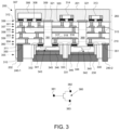
- FIG. 3 is a side, cross-sectional view of the power amplifier device 200 of FIGS. 2 A and 2 B along bisection line 3 , according to an example embodiment.
- the device body includes an encapsulation material layer 260 connected to a substrate 210 .
- the substrate 210 is formed from a stack of multiple dielectric layers 301 , 302 , 303 , 304 , 305 and multiple patterned conductive layers 356 , 357 , 358 , 359 , 360 in an alternating arrangement.
- a lower surface 310 of the substrate partially defines the lower device surface 202 .
- a plurality of conductive vias electrically connect the patterned conductive layers 356 - 360 .
- First and second sets of substrate die contacts 330 , 331 , 332 , 333 are exposed at a first surface 311 of the substrate 210
- additional substrate contacts 320 are exposed at a second surface 312 of the substrate 210 .
- the first set of substrate die contacts includes contacts 330 , 331 that function as I/O contacts for the first power transistor die 340 , and additional contacts that may provide for bias, ground, and control signal connections.
- the first set of substrate die contacts (including contacts 330 , 331 ) are spaced apart from each other, and a “first region” is defined as a portion of the first substrate surface 311 that is located between the first set of substrate die contacts 330 , 331 (e.g., region 890 , FIG. 8 ).
- the second set of substrate die contacts includes contacts 332 , 333 that function as I/O contacts for the second power transistor die 341 , and additional contacts that may provide for bias, ground, and control signal connections.
- the second set of substrate die contacts (including contacts 332 , 333 ) also are spaced apart from each other, and a “second region” is defined as a portion of the first substrate surface 311 that is located between the second set of substrate die contacts 332 , 333 (e.g., region 891 , FIG. 8 ).
- one or more openings in one or more outer layers 305 of the substrate 210 expose one or more portions of the first substrate surface 311 at which the first and second sets of substrate die contacts 330 - 333 are exposed.
- two power transistor dies 340 , 341 are connected to the substrate die contacts 330 - 333 , and thus are connected to the first substrate surface 311 . More particularly, power transistor die 340 is coupled to the first set of substrate die contacts (including contacts 330 , 331 ), and power transistor die 341 is coupled to the second set of substrate die contacts (including contacts 332 , 333 ).
- the first substrate surface 311 is recessed below the lower device surface 202 , and a thermal structure 230 that extends into the die openings thermally couples to the embedded dies 340 , 341 and extends outwardly to define a portion of the lower device surface 202 .
- a first embedded die 340 is a power transistor die that includes at least one integrated transistor 342 (e.g., Si, GaN, SiGe, HEMT, LDMOS, etc.) that functions as the carrier amplifier (e.g., carrier amplifier 130 , 140 , FIG. 1 ).
- a second embedded die 341 also includes at least one integrated power transistor 343 (e.g., Si, GaN, SiGe, HEMT, LDMOS, etc.) that functions as the peaking amplifier (e.g., peaking amplifier 131 , 141 , FIG. 1 ).
- Each die 340 , 341 has an active area, which is defined herein as a portion of the die 340 , 341 that includes the integrated power transistor 342 , 343 .
- the power transistor 380 includes a gate terminal 381 , a drain terminal 382 , and a source terminal 383 .
- the gate and drain terminals of each transistor 342 , 343 are coupled to gate and drain contacts (not numbered) that are exposed at first die surfaces of the dies 340 , 341 .
- the gate and drain contacts are coupled to (e.g., soldered to) the substrate die contacts 330 - 333 .
- each transistor 342 , 343 is coupled to a conductive bottom layer 344 , 345 of each die 340 , 341 , and the conductive bottom layer 344 , 345 defines a second die surface of each die 340 , 341 .
- the gate and/or drain contacts of the dies 340 , 341 may be elongated (e.g., they may have a length dimension that is significantly greater than a width dimension).
- the drain contact of a die 340 , 341 may have a length dimension that is at least five times greater than a width dimension of the drain contact.
- each of the substrate die contacts 330 - 333 are shaped and sized to correspond to the shape and size of the gate or drain contact to which the substrate die contact 330 - 333 is connected.
- the substrate die contacts 330 - 333 also may be elongated, and further may have shapes and sizes that ensure good connection along the entire lengths of the gate and/or drain contacts of the dies 340 , 341 .
- a first air cavity 390 extends into the substrate 210 through the first region of the substrate surface 311 (e.g., region 890 , FIG. 8 ).
- a second air cavity 391 extends into the substrate 210 through the second region of the substrate surface 311 (e.g., region 891 , FIG. 8 ).
- the air cavities 390 , 391 may produce the beneficial result of reducing parasitic impacts (e.g., performance degradation of active and passive circuits), which otherwise may result from the proximity of the dies 340 , 341 to the substrate material.
- Each of the first and second air cavities 390 , 391 has a proximal end at the first substrate surface 311 , a distal end that is recessed within the substrate 210 , and sidewalls extending between the proximal and distal ends.
- the proximal end of each air cavity 390 , 391 is defined by an opening in the first substrate surface 311 .
- each opening has an area that is smaller than the die footprint (e.g., die footprint 840 , 841 , FIG. 1 ), and that is equal to or smaller than the area of the first or second region (e.g., regions 890 , 891 , FIG. 8 ).
- each opening has an area that is at least one tenth of the size of the die footprint (e.g., from one tenth to one half of the die footprint size). In other embodiments, each opening may have an area that is at least one half of the size of the die footprint.
- each of the active areas of the dies 340 , 341 is aligned with one of the first or second air cavities 390 , 391 (i.e., the first and second air cavities 390 , 391 are positioned directly over the active areas of the power transistor devices 340 , 341 ).
- each of the first and second air cavities 390 , 391 may extend from the first substrate surface 311 through all of the multiple dielectric layers 301 - 304 to substrate surface 312 .
- the first and second air cavities may extend from the first substrate surface 311 through at least one but fewer than all of the multiple dielectric layers 301 - 304 .
- conductive (metal) caps 321 are located at and extend across the distal ends of the first and second air cavities 390 , 391 .
- the conductive caps 321 may be formed from portions of patterned conductive layer 356 (or another conductive layer).
- the conductive caps 321 may be metal coins that are attached to the upper surface 312 of substrate 210 over each air cavity 390 , 391 .
- the conductive caps 321 may be electrically floating, or may be coupled to a ground reference, in various embodiments.
- the conductive caps 321 may provide the advantage of mitigating electromagnetic interference from the power transistor dies 340 , 341 that may otherwise detrimentally affect the performance of the various active and passive circuits that also are included in device 200 (e.g., circuits that include surface mount devices 306 , 313 , 314 , among others).
- a thermal structure 230 extends into the opening (or openings) of the outermost substrate layer(s) 305 , and is coupled (e.g., using die attach 346 , solder, or other suitable conductive materials) to the conductive bottom layers 344 , 345 of the power transistor dies 340 , 341 .
- die attach 346 solder, or other suitable conductive materials
- the thickness of the die attach 346 may be different between each die 340 , 341 and the thermal structure 230 .
- the thermal structure 230 could be machined so that portions of the structure 230 that are coupled to the dies 340 , 341 (e.g., “pedestals”) have different heights to accommodate the different die heights.
- portions of the structure 230 that are coupled to the dies 340 , 341 e.g., “pedestals”
- the pedestal heights are configured so that each pedestal is the same distance from the corresponding die, the thickness of the die attach 346 can be the same for both dies 340 , 341 .
- the outer surface of the thermal structure 230 corresponds to a portion of the lower surface 202 of the device 200 .
- the thermal structure 230 is configured to convey heat generated by the dies 340 , 341 away from the dies 340 , 341 , and to an external system heat sink (e.g., heat extraction component 1330 or 1430 , FIGS. 13 , 14 ) associated with an amplifier system (e.g., a transmitter of a communication system).
- an external system heat sink e.g., heat extraction component 1330 or 1430 , FIGS. 13 , 14
- an amplifier system e.g., a transmitter of a communication system
- a plurality of conductive interconnects 240 - 1 , 240 - 2 (e.g., interconnects 240 , FIG. 2 ) have distal ends exposed at the lower device surface 202 .
- the conductive interconnects 240 - 1 , 240 - 2 extend through the outermost substrate layer(s) 305 , and their proximal ends are electrically connected to the patterned conductive layers 356 - 360 of the substrate 210 . These connections may be made through interconnect contacts 350 , 351 .
- the interconnect contacts 350 , 351 may be positioned at the first substrate surface 311 .
- the conductive interconnects 240 ( FIG.
- conductive interconnect 240 - 1 more specifically corresponds to an RF input terminal (e.g., terminal 102 , FIG. 1 ), and conductive interconnect 240 - 2 more specifically corresponds to an RF output terminal (e.g., terminal 104 , FIG. 1 ).
- the one or more surface mount components 306 , 313 , 314 are connected to additional substrate contacts 320 that are exposed at a second surface 312 of the substrate 210 .
- the encapsulation material layer 260 covers the surface mount components 306 , 313 , 314 and the second substrate surface 312 .
- the encapsulation material layer 260 essentially defines the upper device surface 201 . According to an embodiment, sidewalls of the substrate 210 and the encapsulation material layer 260 that are on the same side of the device 200 are co-planar.
- the surface mount components 306 , 313 , 314 can correspond to a number of components of an amplifier circuit (e.g., pre-amplifier transistors, power splitting circuitry, harmonic termination circuitry, inductors, capacitors, and impedance matching circuitry).
- at least one surface mount component 306 may correspond to a power divider circuit (e.g., power divider 106 , FIG. 1 ), which has an input terminal 307 (e.g., terminal 107 , FIG. 1 ) and multiple output terminals 308 , 309 (e.g., terminals 108 , 109 , FIG. 1 ).
- the power divider input terminal 307 is electrically coupled through a conductive path formed from portions of the patterned conductive substrate layers 356 - 360 and vias (e.g., via 315 ) to one of the conductive interconnects 240 - 1 , which corresponds to the input terminal (e.g., input terminal 102 , FIG. 1 ) of the amplifier.
- the power divider circuit 306 also may have at least two output terminals 308 , 309 , where each output terminal is coupled to one of the inputs (e.g., drain terminals) of the transistors 342 , 343 within the power transistor dies 340 , 341 .
- the output terminals 308 , 309 of the power divider circuit 306 may be coupled to the inputs of the power transistor dies 340 , 341 directly through conductive paths formed by the patterned conductive layers 356 - 360 and vias (e.g., via 315 ).
- the output terminals 308 , 309 of the power divider circuit 306 may be coupled through conductive paths in the substrate 210 to additional surface mount components 313 , 314 , which correspond to portions of input impedance matching circuits (e.g., circuits 113 , 114 , FIG. 1 ).
- Those additional surface mount components 313 , 314 may be coupled to the inputs of the power transistor dies 340 , 341 directly through conductive paths formed by the patterned conductive layers 356 - 360 and vias (e.g., via 315 ). Note that, in FIG. 3 and other figures described later, some conductive paths are indicated with dashed lines.
- the input RF signal may be conveyed through the substrate 210 to the input terminal 307 of the power divider circuit 306 , and the power divider circuit 306 may perform the function of splitting the input RF signal into multiple (e.g., two or more) separate signals (e.g., a carrier signal and a peaking signal).
- the separate signals provided at the power divider outputs 308 , 309 may then be conveyed through the substrate 210 to the impedance matching components 313 , 314 or directly to the inputs of the power transistor dies 340 , 341 .
- the power divider circuit 306 is shown as a single surface-mount component, in other embodiments, multiple surface mount components may be used to implement the power divider circuit 306 .
- At least one additional surface-mount component may be used to implement a harmonic termination circuit (e.g., harmonic termination circuits 116 , 118 , FIG. 1 ) coupled between each amplification path and ground.
- a harmonic termination circuit e.g., harmonic termination circuits 116 , 118 , FIG. 1
- a harmonic termination circuit includes a shunt LC circuit
- at least part of the inductance (L) can be implemented using a series of conductive traces and vias of the patterned conductive layers 356 - 360
- another part of the inductance (L) can be implemented with a surface mount component coupled to contacts at substrate surface 312
- the capacitance (C) can be a surface mount component coupled to additional contacts at substrate surface 312 .
- the inductance (L) and capacitance (C) can be coupled in series through the patterned conductive layers 356 - 360 .
- An input to each LC circuit can be coupled to a point along each of the amplification paths (e.g., a point before or after each power transistor), and an output to each LC circuit can be coupled through the patterned conductive layers 356 - 360 to another one of the conductive interconnects 240 .
- that conductive interconnect 240 can be coupled to ground.
- a phase delay element (e.g., phase delay element 182 , FIG. 1 ) is coupled between the power divider 106 and the input to the peaking amplifier 131 , 141 .
- the phase delay element (e.g., phase delay element 182 , FIG. 1 ) may be implemented using a conductive path through the substrate 210 , which electrically couples an output of the power divider circuit 306 to an input (e.g., gate terminal) of the peaking amplifier die (e.g., the terminal of die 341 coupled to substrate contact 332 ).
- the conductive path corresponding to the phase delay element may have an electrical length of about 90 degrees, according to an embodiment.
- the outputs of the carrier and peaking power amplifiers 140 , 141 each are coupled to a combining node 180 .
- the combining node is designed to be co-located with the output terminal (e.g., drain terminal) of the peaking amplifier die (e.g., the terminal of die 341 coupled to substrate contact 333 ).
- the impedance inverter/phase delay element e.g., impedance inversion/phase delay element 184 , FIG.
- the output terminal of the carrier amplifier die 340 is electrically connected to the output terminal of the peaking amplifier die 341 through vias 316 , 317 and conductive trace 318 (i.e., a portion of patterned conductive layer 359 ).
- interconnect 240 - 2 functions as the output terminal of the amplifier device, and the output terminal (e.g., drain terminal) of the peaking amplifier die 341 is electrically coupled to interconnect 240 - 2 through a conductive path (indicated with a dashed line) through the substrate 210 .
- some conductive interconnects 240 may be used to receive bias voltages, which may be conducted from the interconnects 240 to the power transistor dies 340 , 341 through the patterned conductive layers 356 - 360 and conductive vias of the substrate 210 .
- other conductive interconnects 240 may be used to provide a ground reference (e.g., they may be coupled to ground when device 200 is incorporated into a larger system).
- the ground connection between the ground interconnects 240 and other circuit components e.g., some of surface mount devices 306 , 313 , 314 ) may be made through the patterned conductive layers 356 - 360 and conductive vias of the substrate 210 .
- Still other conductive interconnects 240 may be used to convey control signals to components within device 200 .
- the power amplifier device 200 illustrated in FIGS. 2 and 3 may encompass a full Doherty amplifier circuit in a compact package. It may be noted that no wirebond arrays are used to interconnect the components of the Doherty amplifier. Therefore, in comparison with conventional Doherty amplifier circuits, the lack of wirebond arrays may result in increased amplifier power and efficiency. Further, minimized inductances inherent in the Doherty device embodiments described herein may enable compliance with higher band specifications.
- FIG. 4 is a flowchart of a method 400 of manufacturing the power amplifier device 200 of FIGS. 2 and 3 , according to an example embodiment.
- FIG. 4 should be viewed simultaneously with FIGS. 5 - 12 , which are side, cross-sectional views of the power amplifier device of FIGS. 2 and 3 at various stages of manufacture, according to an embodiment.
- the method begins, in step 402 , by fabricating a multi-layer substrate 210 .
- the substrate 210 is formed from a stack of multiple dielectric layers 301 - 305 and multiple patterned conductive layers 356 - 360 , which are built up in an alternating arrangement.
- the substrate 210 is defined by a lower surface 310 , an upper surface 312 , and sidewalls extending between the lower and upper surfaces 310 , 312 .
- the dielectric layers 301 - 305 may be formed from PCB dielectric materials (e.g., FR-4), ceramic, or other suitable dielectric materials.
- the patterned conductive layers 356 - 360 are formed from conductive metals, which are patterned during the build-up process. Also during the build-up process, conductive vias (e.g., vias 315 - 317 , FIG. 3 ) are formed through the dielectric layers in order to connect various portions of adjacent patterned conductive layers.
- conductive caps 321 may be attached to the upper surface 312 of the substrate 210 in locations that correspond to the distal ends of the (to be formed) air cavities (e.g., air cavities 390 , 391 , FIG. 3 ).
- the conductive caps 321 may be formed from portions of the patterned conductive layer (e.g., layer 356 ) where the distal ends of the air cavities will be located.
- the conductive caps 321 may be attached to the upper surface 312 of the substrate 210 after forming the air cavities 390 , 391 (e.g., after step 406 , discussed below).
- Various conductive paths within the substrate 210 will provide for interconnections between dies and components, which will later be mounted to the substrate 210 .
- some of the conductive paths within the substrate may be configured to provide desired inductances and impedance transformations.
- a conductive path comprising vias 316 , 317 and conductive layer portion 318 may form a phase delay and impedance inverter element (e.g., impedance inverter/phase delay element 184 , FIG. 1 ).
- substrate 210 is shown to include five dielectric layers 301 - 305 and five conductive layers 356 - 360 , other embodiments of a substrate may include more or fewer dielectric layers and/or conductive layers.
- the substrate 210 includes substrate contacts 320 , which are exposed at the upper surface 312 of the substrate 210 .
- the substrate includes embedded substrate die contacts 330 - 333 and embedded interconnect contacts 350 , 351 at an internal, surface 311 of the substrate 210 .
- step 404 by creating one or more first die openings 602 through the lower substrate surface 310 to expose substrate die contacts 330 - 333 at the interior surface 311 of the substrate 210 .
- second interconnect openings 604 are formed through the lower substrate surface 310 to expose interconnect contacts 350 , 351 , which also may be located at the interior surface 311 .
- the openings 602 , 604 may be formed using an etching process, which is timed to stop when the substrate and interconnect contacts 330 - 333 , 350 , 351 are reached.
- FIG. 6 illustrates that two die openings 602 are formed in substrate 210 , in alternate embodiments, a single opening may be formed, which will accommodate both power transistor dies 340 , 341 .
- interconnect openings 604 may form a separate opening for each interconnect 240
- other embodiments may include forming a larger opening that spans multiple interconnect contacts, and into which multiple interconnects 240 may be inserted.
- FIGS. 7 and 8 are cross-sectional and bottom views of device 200 , respectively, at a same fabrication stage, the method continues, in step 406 , by creating air cavities 390 , 391 in the substrate between each set of substrate contacts (e.g., within each of regions 890 , 891 , FIG. 8 ).
- the previously-discussed first and second regions 890 , 891 between sets of die contacts, and the approximate footprints 840 , 841 of the to-be-connected dies 340 , 341 are indicated with dashed-line boxes.
- the air cavities 390 , 391 may be formed in regions 890 , 891 using an etching process, which is timed to stop when the conductive caps 321 are reached.
- the air cavity openings 390 , 391 may be formed to extend all the way through the substrate 210 , and the conductive caps 321 can be attached over the openings 390 , 391 thereafter.
- each of the first and second air cavities 390 , 391 has a proximal end at the first substrate surface 311 , a distal end that is recessed within the substrate 210 (and co-located with caps 321 ), and sidewalls extending between the proximal and distal ends.
- the proximal end of each air cavity 390 , 391 is defined by an opening in the first substrate surface 311 .
- the conductive caps 321 can be seen at the bottom of each air cavity 390 , 391 .
- each opening (or the cross-section of each cavity 390 , 391 ) has an area that is smaller than the die footprint (e.g., die footprint 840 , 841 ), and that is equal to or smaller than the area of the first or second region 890 , 891 .
- each opening has an area that is at least one tenth of the size of the die footprint 840 , 841 (e.g., from one tenth to one half of the die footprint size). In other embodiments, each opening may have an area that is at least one half of the size of the die footprint.
- conductive interconnects 240 are physically and electrically coupled to the interconnect contacts 350 , 351 exposed through the interconnect openings 604 .
- the conductive interconnects 240 are conductive posts that are inserted into the interconnect openings 604 , and then soldered, brazed, or otherwise attached to the interconnect contacts 350 , 351 .
- the conductive interconnects 240 may be formed by filling the interconnect openings 604 with conductive material.
- the interconnects 240 may be portions of a leadframe (not shown).
- multiple interconnects 240 may be packaged side-by-side in one or more separate dielectric interposer structures (not shown), and the dielectric interposer structures may be inserted into larger interconnect openings that span multiple interconnect contacts 350 , 351 . As shown in FIG. 2 B , the interconnect openings and the interconnect contacts 240 may be located adjacent to multiple sides of the device 200 (e.g., to all four sides, as shown, or to less than all four sides).
- the power transistor dies 340 , 341 are “bumped,” by applying solder paste to the die bondpads (e.g., to the input and output, or gate and drain, bondpads).
- the dies are then inserted into the die openings 602 .
- the die bondpads and the solder paste on the die bondpads are brought into contact with corresponding substrate die contacts 330 - 333 .
- a solder reflow process may then be performed to solder-attach the die bondpads to the substrate die contacts 330 - 333 .
- the active areas of the dies 340 , 341 should be aligned with the air cavities 390 , 391 , respectively.
- gaps between the power transistor dies 340 , 341 and sidewalls of the die openings 602 are then filled in with fill material 902 (e.g., plastic encapsulant material).
- the fill material 902 is applied so that it fills the gaps between the sidewalls of the dies 340 , 341 and the sidewalls of openings 602 , but so that it does not flow into air cavities 390 , 391 .
- the fill material 902 may be deposited so that it only extends part-way up the sides of the dies 340 , 341 , leaving the outer surface of the die (e.g., conductive layer 344 , 345 ) exposed. In other embodiments, as indicated in FIG.
- a sufficient quantity of the fill material 902 may be deposited in the openings 602 so that the fill material 902 completely covers the power transistor dies 340 , 341 .
- portions of the fill material 902 subsequently may be removed, as indicated by dashed lines in the fill material 902 , to expose the conductive layers 344 , 345 on the outward facing surface of the power transistor dies 340 , 341 .
- the conductive layers 344 , 345 that define the exposed outer surfaces of the dies 340 , 341 may be electrically connected, within each die 340 , 341 , to a source terminal of a transistor embedded within the die 340 , 341 .
- electrically and thermally conductive die attach material 346 (e.g., solder paste, sinter paste, or other suitable materials) is applied to the outward facing surfaces of the dies 340 , 341 , and more particularly to the conductive layers 344 , 345 of the dies 340 , 341 .
- the thickness of the die attach material 346 over each die 340 , 341 may be different to account for differing heights of the dies 340 , 341 .
- the thickness of the die attach material 346 over each die 340 , 341 may be the same, and height differences may be accommodated by customizing the subsequently attached thermal structure 230 .
- the thermal structure 230 may be a simple conductive coin, or as illustrated in FIGS. 10 and 11 , may have a more complicated configuration.
- the thermal structure 230 may be a cast or machined piece of thermally conductive material (e.g., metal), which has a base 1002 and multiple pedestals 1004 , 1006 that establish equal or differing thicknesses across the thermal structure 230 .
- the pedestals 1004 , 1006 have equal heights (vertical dimension in FIGS. 10 , 11 ).
- the multiple pedestals 1004 , 1006 may have different heights. This may be desirable, for example, so that equal thickness of die attach material 346 may be deposited on each die 340 , 341 , and the die height variation may be accommodated by the different-height pedestals.
- the thermal structure 230 is then inserted into the die openings 602 and brought into contact with the die attach material 346 .
- the device 200 is then processed (e.g., by performing a reflow or sintering process) to securely connect the thermal structure 230 to the dies 340 , 341 .
- the terminals of one or more surface mount components 306 , 313 , 314 are coupled (e.g., solder-attached) to the additional substrate contacts 320 that are exposed at substrate surface 312 .
- the surface mount components 306 , 313 , 314 can correspond to a number of components of an amplifier circuit.
- surface mount component 306 may correspond to a power divider circuit (e.g., power divider 106 , FIG. 1 ), and surface mount components 313 , 314 may correspond to capacitors, inductors, or other circuit elements associated with impedance matching, harmonic termination, and so on.
- Portions of the patterned conductive layers 356 - 360 also may correspond to circuit elements associated with the impedance matching and harmonic termination circuits.
- various conductive traces and vias of layers 356 - 360 may provide inductances of the impedance matching and harmonic termination circuits.
- conductive stubs e.g., radial stubs
- conductive stubs can be configured to match a load impedance to the transmission line characteristic impedance.
- one or more stubs may be positioned along conductive paths at various locations. Each stub may be made capacitive or inductive according to whether the conductive path to which it is coupled presents an inductive or capacitive impedance, respectively.
- the device 200 is completed in step 418 by applying an encapsulation material layer 260 (e.g., molding compound) over substrate surface 312 and the surface-mount components 306 , 313 , 314 coupled to substrate surface 312 .
- the encapsulation material layer 260 defines the upper surface 201 of the device 200
- the lower substrate surface 310 and the thermal structure 230 define the lower surface 202 of the device 200 .
- FIG. 13 is side, cross-sectional view of the power amplifier device 200 of FIG. 3 coupled to a system substrate 1310 , according to an example embodiment.
- the system substrate 1310 may be, for example, a PCB with a plurality of contact pads 1320 , 1322 at a top surface 1312 .
- the contact pads 1320 , 1322 may be electrically coupled through additional traces on the substrate 1310 to other system components.
- a heat sink or heat extraction component 1330 (e.g., a conductive coin, thermal vias, or other thermally conductive component) is embedded within the system substrate 1310 , and has an exposed upper surface proximate the top surface 1312 of the system substrate 1310 .
- Device 200 is physically and electrically coupled to the system substrate 1310 . More particularly, and according to an embodiment, the thermal structure 230 of device 200 is physically, electrically, and thermally coupled to the heat extraction component 1330 of the system substrate 1310 .
- thermal structure 230 and heat extraction component 1330 may be coupled together using thermal grease, solder, sinter material, or brazing. Besides providing a pathway for extraction of heat, the heat extraction component 1330 also may be coupled to system ground, and thus the heat extraction component 1330 may serve as a system ground connection for device 200 .
- the conductive interconnects 240 - 1 , 240 - 2 are physically and electrically coupled (e.g., soldered) to the contact pads 1320 , 1322 at the top surface 1312 of the system substrate 1310 .
- the system substrate 1310 enables RF input signals to be provided to device 200 (e.g., through contact pad 1320 ), RF output signals to be received from device 200 (e.g., through contact pad 1322 ), and additional bias and ground connections to be established between the system substrate 1310 and the device 200 through other substrate contact pads and device interconnects (not shown).
- the embodiment of device 200 depicted in FIGS. 3 and 13 provides for bottom-side cooling of device 200 .
- a bottom-side cooled system such as that depicted in FIG. 13 , the heat extraction path for the dies 340 , 341 within device 200 extends through the system substrate 1310 .
- FIG. 14 is a side, cross-sectional view of another embodiment of a power amplifier device 200 ′ coupled to a system substrate 1410 in a system with top-side heat extraction, according to an example embodiment.
- Device 200 ′ shown in FIG. 14 is slightly different from device 200 in FIGS. 3 and 13 to facilitate incorporation into a top-side cooled system.
- device 200 includes conductive interconnects 240 - 1 , 240 - 2 that extend through though a layer 305 located at the lower surface 310 of the device substrate 210 .
- the conductive interconnects 240 - 1 , 240 - 2 and the thermal structure 230 both are exposed at the lower surface 310 of the device 200 .
- conductive interconnects 240 - 3 , 240 - 4 which function as I/O terminals for the device 200 ′, instead are coupled to surface 312 of device substrate 210 , and the interconnects 240 - 3 , 240 - 4 extend through the encapsulation material layer 260 at the opposite surface of the device 200 ′ from the dies 340 , 341 and the thermal structure 230 . Additional conductive interconnects (not shown) for bias and ground connection also would extend through the encapsulation material layer 260 .
- the conductive interconnects 240 - 3 , 240 - 4 are exposed at an opposite surface of device 200 ′ than the surface at which the thermal structure 230 is exposed.
- the conductive interconnects 240 - 3 , 240 - 4 are electrically coupled through the device substrate to the various dies 340 , 341 and surface mount components 306 , 313 , 314 as discussed above in conjunction with FIG. 3 .
- system substrate 1410 may be, for example, a PCB with a plurality of contact pads 1420 , 1422 at a top surface 1412 .
- the contact pads 1420 , 1422 may be electrically coupled through additional traces on the substrate 1410 to other system components.
- Device 200 ′ is physically and electrically coupled to the system substrate 1410 . More particularly, and according to an embodiment, the conductive interconnects 240 - 3 , 240 - 4 (and other interconnect, not shown) are physically and electrically coupled (e.g., soldered) to the contact pads 1420 , 1422 at the top surface 1412 of the system substrate 1410 . Accordingly, the system substrate 1410 enables RF input signals to be provided to device 200 ′ (e.g., through contact pad 1420 ), RF output signals to be received from device 200 ′ (e.g., through contact pad 1422 ), and additional bias and ground connections to be established between the system substrate 1410 and the device 200 ′ through other substrate contact pads and device interconnects (not shown).
- the conductive interconnects 240 - 3 , 240 - 4 are physically and electrically coupled (e.g., soldered) to the contact pads 1420 , 1422 at the top surface 1412 of the system substrate 1410 .
- the system substrate 1410
- a heat extraction component 1430 e.g., a heat sink or conductive plate
- thermal structure 230 and heat extraction component 1430 may be coupled together using thermal grease, solder, sinter material, or brazing.
- the heat extraction component 1430 also may be coupled to system ground, and thus the heat extraction component 1430 may serve as a system ground connection for device 200 ′.
- grounding structures may be implemented within device 200 ′ (e.g., by providing a conductive pathway through the substrate 210 between conductive layers 344 , 345 and a device terminal 240 coupled to system ground), or on the exterior surface of device 200 ′ (e.g., by providing a conductive pathway extending along the sides of substrate 210 and layer 260 that electrically couples layers 344 , 345 to a ground contact on the system substrate 1410 ).
- FIG. 15 is a side, cross-sectional view of another power amplifier device 200 ′′ with air cavities 1590 , 1591 that only partially extend through substrate 1510 , according to another example embodiment. Except for the modified air cavities 1590 , 1591 , substrate 1510 is identical to substrate 210 .
- each air cavity 1590 , 1591 extends from substrate surface 311 through only one dielectric layer 304 , with a cap 1521 located at the distal end of each air cavity 1590 , 1591 .
- the caps 1521 may be formed from portions of conductive layer 359 , for example.
- the air cavities may extend through more than one dielectric layer, with the distal end cap being formed from a portion of whichever patterned conductive layer corresponds to the distal end of the air cavity.
- power transistor devices 200 , 200 ′, 200 ′′ Other types of modifications also may be made to power transistor devices 200 , 200 ′, 200 ′′.
- the power transistor dies 340 , 341 instead could be coupled to a substrate surface and encapsulated.
- FIG. 16 is a side, cross-sectional view of another example embodiment of a power amplifier device 1600 .
- Power amplifier device 1600 is similar in many respects to power amplifier devices 200 , 200 ′, 200 ′′ ( FIGS. 3 , 14 , 15 ), discussed above. Where elements in power amplifier device 1600 are substantially identical to elements in power amplifier devices 200 , 200 ′, 200 ′′ the same reference numbers will be used, and all details discussed above with respect to such elements apply equally to the same-numbered elements in FIG. 16 . For purpose of brevity, all details will not be repeated here.
- the device body includes first and second encapsulation material layers 260 , 1660 connected to opposite surfaces 1612 , 1611 of a substrate 1610 .
- the substrate 1610 is formed from a stack of multiple dielectric layers 301 - 304 and multiple patterned conductive layers 356 - 360 in an alternating arrangement.
- a plurality of conductive vias (e.g., via 315 ) electrically connect the patterned conductive layers 356 - 360 .
- Substrate die contacts 330 - 333 and interconnect contacts 350 , 351 are exposed at a first surface 1611 of the substrate 1610 , and additional substrate contacts 320 are exposed at a second surface 1612 of the substrate 1610 .
- the substrate 1610 includes air cavities 390 , 391 that extend from substrate surface 1611 through dielectric layers 301 - 304 , along with a conductive cap 321 at the distal end of each air cavity 390 , 391 .
- one or more surface mount components 306 , 313 , 314 are connected to the additional substrate contacts 320 that are exposed at the second surface 1612 of the substrate 1610 .
- a first encapsulation material layer 260 covers the surface mount components 306 , 313 , 314 and the second substrate surface 1612 .
- the first encapsulation material layer 260 essentially defines the upper device surface 1601 .
- the surface mount components 306 , 313 , 314 can correspond to a number of components of an amplifier circuit.
- at least one surface mount component 306 may correspond to a power divider circuit (e.g., power divider 106 , FIG. 1 )
- additional surface mount components 313 , 314 may correspond to portions of input impedance matching circuits (e.g., circuits 113 , 114 , FIG. 1 ) and/or harmonic termination circuits (e.g., circuits 116 , 118 , FIG. 1 ).
- first and second power transistor dies 340 , 341 are connected to the substrate die contacts 330 - 333 , and thus are connected to the first substrate surface 1611 .
- the first power transistor die 340 includes at least one integrated transistor 342 in an active area of die 340
- the second power transistor die 341 includes at least one additional integrated transistor 343 in an active area of die 341 .
- Each power transistor includes a gate terminal, a drain terminal, and a source terminal. As can be seen in the cross-section of device 1600 , the gate and drain terminals of each transistor 342 , 343 are coupled to gate and drain contacts (not numbered) that are exposed at first die surfaces of the dies 340 , 341 .
- the gate and drain contacts are coupled to (e.g., soldered to) the substrate die contacts 330 - 333 .
- the source terminal of each transistor 342 , 343 is coupled to a conductive bottom layer 344 , 345 of each die 340 , 341 , and the conductive bottom layer 344 , 345 defines a second die surface of each die 340 , 341 .
- proximal ends of a plurality of conductive interconnects 1640 - 1 , 1640 - 2 are coupled to interconnect contacts 350 , 351 at the first surface 1611 of the substrate. Similar to the conductive interconnects 240 - 1 , 240 - 2 of FIG.
- the conductive interconnects 1640 - 1 , 1640 - 2 of the power transistor device 1600 are configured to convey RF signals, bias voltages, and ground connections to the amplifier circuitry (e.g., dies 340 , 341 and surface mount components 306 , 313 , 314 ) embedded within the device 1600 .
- conductive interconnect 1640 - 1 more specifically corresponds to an RF input terminal (e.g., terminal 102 , FIG. 1 )
- conductive interconnect 1640 - 2 more specifically corresponds to an RF output terminal (e.g., terminal 104 , FIG. 1 ).
- power transistor device 1600 includes a second encapsulation material layer 1660 that covers the first surface 1611 , sidewalls of the power transistor dies 340 , 341 and sidewalls of the conductive interconnects 1640 - 1 , 1640 - 2 .
- the second encapsulation material layer 1660 essentially defines the lower device surface 1602 .
- the conductive layers 344 , 345 of the power transistor dies 340 , 341 are exposed at the lower device surface 1602 , as are the distal ends of the conductive interconnects 1640 - 1 , 1640 - 2 .
- the input RF signal may be conveyed through the substrate 1610 to the input terminal of the power divider circuit 306 , and the power divider circuit 306 may perform the function of splitting the input RF signal into multiple (e.g., two or more) separate signals (e.g., a carrier signal and a peaking signal).
- the separate signals provided at the power divider outputs may then be conveyed through the substrate 1610 to the impedance matching components 313 , 314 or directly to the inputs of the power transistor dies 340 , 341 .
- conductive interconnects may be used to receive bias voltages, which may be conducted from the interconnects to the power transistor dies 340 , 341 through the patterned conductive layers 356 - 360 and conductive vias of the substrate 1610 .
- other conductive interconnects may be used to provide a ground reference (e.g., they may be coupled to ground when device 1600 is incorporated into a larger system).
- the ground connection between the ground interconnects and other circuit components may be made through the patterned conductive layers 356 - 360 and conductive vias of the substrate 1610 .
- FIG. 17 is a flowchart of a method 1700 of manufacturing the power amplifier device 1600 of FIG. 16 , according to an example embodiment.
- FIG. 17 should be viewed simultaneously with FIGS. 18 and 19 , which are side, cross-sectional views of the power amplifier device 1600 of FIG. 16 at various stages of manufacture, according to an embodiment.
- the method begins, in step 1702 , by fabricating a multi-layer substrate 1610 .
- the substrate 1610 is formed from a stack of multiple dielectric layers 301 - 304 and multiple patterned conductive layers 356 - 360 , which are built up in an alternating arrangement.
- the substrate 1610 is defined by a lower surface 1611 , an upper surface 1612 , and sidewalls extending between the lower and upper surfaces 1611 , 1612 .
- the dielectric layers 301 - 304 may be formed from PCB dielectric materials (e.g., FR-4), ceramic, or other suitable dielectric materials.
- the patterned conductive layers 356 - 360 are formed from conductive metals, which are patterned during the build-up process. Also during the build-up process, conductive vias (e.g., vias 315 - 317 ) are formed through the dielectric layers in order to connect various portions of adjacent patterned conductive layers.
- Various conductive paths within the substrate 1610 will provide for interconnections between dies and components, which will later be mounted to the substrate 1610 .
- some of the conductive paths within the substrate may be configured to provide desired inductances and impedance transformations.
- a conductive path comprising vias 316 , 317 and conductive layer portion 318 may form a phase delay and impedance inverter element (e.g., impedance inverter/phase delay element 184 , FIG. 1 ).
- substrate 1610 is shown to include four dielectric layers 301 - 304 and five conductive layers 356 - 360 , other embodiments of a substrate may include more or fewer dielectric layers and/or conductive layers.
- the substrate 1610 includes substrate contacts 320 , which are exposed at the upper surface 1612 of the substrate 1610 .
- the substrate includes substrate die contacts 330 - 333 and interconnect contacts 350 , 351 exposed at the lower surface 1611 of the substrate 1610 .
- air cavities 390 , 391 also are formed in the substrate in step 1704 .
- the air cavities 390 , 391 are formed in the substrate between each set of substrate contacts (e.g., within each of regions 890 , 891 , FIG. 8 ).
- the air cavities 390 , 391 may be formed in regions 890 , 891 using an etching process, which is timed to stop when the conductive caps 321 are reached.
- the air cavity openings 390 , 391 may be formed to extend all the way through the substrate 1610 , and the conductive caps 321 can be attached over the air cavities 390 , 391 thereafter.
- each of the first and second air cavities 390 , 391 has a proximal end at the first substrate surface 1611 , a distal end that is recessed within the substrate 1610 (and co-located with caps 321 ), and sidewalls extending between the proximal and distal ends.
- the proximal end of each air cavity 390 , 391 is defined by an opening in the first substrate surface 1611 .
- each air cavity opening (or the cross-section of each cavity 390 , 391 ) has an area that is smaller than the die footprint (e.g., die footprint 840 , 841 ), and that is equal to or smaller than the area of the first or second region 890 , 891 .
- each opening has an area that is at least one tenth of the size of the die footprint 840 , 841 (e.g., from one tenth to one half of the die footprint size). In other embodiments, each opening may have an area that is at least one half of the size of the die footprint.
- conductive interconnects 1640 - 1 , 1640 - 2 are physically and electrically coupled to the interconnect contacts 350 , 351 exposed at the lower surface 1611 of the substrate 1610 .
- the interconnect contacts 1640 - 1 , 1640 - 2 are conductive posts that are soldered, brazed, or otherwise attached to the interconnect contacts 350 , 351 .
- the interconnect contacts 1640 - 1 , 1640 - 2 may be portions of a leadframe (not shown).
- multiple interconnects may be packaged side-by-side in one or more separate dielectric interposer structures (not shown), and the dielectric interposer structures may be coupled to the interconnect contacts 350 , 351 .
- the power transistor dies 240 , 241 are “bumped,” by applying solder paste to the die bondpads (e.g., to the input and output, or gate and drain, bondpads).
- the die bondpads and the solder paste on the die bondpads are brought into contact with corresponding substrate die contacts 330 - 333 .
- a solder reflow process may then be performed to solder-attach the die bondpads to the substrate die contacts 330 - 333 .
- the terminals of one or more surface mount components 306 , 313 , 314 are coupled (e.g., solder-attached) to the additional substrate contacts 320 that are exposed at substrate surface 1612 .
- the surface mount components 306 , 313 , 314 can correspond to a number of components of an amplifier circuit.
- surface mount component 306 may correspond to a power divider circuit (e.g., power divider 106 , FIG. 1 ), and surface mount components 313 , 314 may correspond to capacitors, inductors, or other circuit elements associated with impedance matching, harmonic termination, and so on.
- an encapsulation material layer 260 (e.g., molding compound) is applied over substrate surface 1612 and the surface-mount components 306 , 313 , 314 coupled to substrate surface 1612 .
- the encapsulation material layer 260 defines the upper surface 1601 of the device 1600 .
- the device is completed, in step 1714 , by applying another encapsulation material layer 1660 (e.g., molding compound) over substrate surface 1611 , dies 340 , 341 , and interconnects 1640 - 1 , 1640 - 2 , according to an embodiment.
- the encapsulation material layer 1660 defines the lower surface 1602 of the device 1600 .
- the distal ends of interconnects 1640 - 1 , 1640 - 2 and the conductive bottom layers 344 , 345 of the dies 340 , 341 are exposed at the lower surface 1602 of the device 1600 .
- the conductive layers 344 , 345 that define the exposed outer surfaces of the dies 340 , 341 may be electrically connected, within each die 340 , 341 , to a source terminal of a transistor embedded within the die 340 , 341 .
- FIG. 20 is a side, cross-sectional view of the power amplifier device 1600 of FIG. 16 coupled to a system substrate 2010 , according to an example embodiment.
- the system substrate 2010 may be, for example, a PCB with a plurality of contact pads 2020 , 2022 at a top surface 2012 .
- the contact pads 2020 , 2022 may be electrically coupled through additional traces on the substrate 2010 to other system components.
- a heat sink or heat extraction component 2030 (e.g., a conductive coin, thermal vias, or other thermally conductive component) is embedded within the system substrate 2010 , and has an exposed upper surface proximate the top surface 2012 of the system substrate 2010 .
- Device 1600 is physically and electrically coupled to the system substrate 2010 . More particularly, and according to an embodiment, the conductive surfaces 344 , 345 of dies 340 , 341 are physically, electrically, and thermally coupled to the heat extraction component 2030 of the system substrate 2010 .
- dies 340 , 341 and heat extraction component 2030 may be coupled together using thermal grease, solder, sinter material, or brazing. Besides providing a pathway for extraction of heat, the heat extraction component 2030 also may be coupled to system ground, and thus the heat extraction component 2030 may serve as a system ground connection for device 1600 .
- the conductive interconnects 1640 - 1 , 1640 - 2 are physically and electrically coupled (e.g., soldered) to the contact pads 2020 , 2022 at the top surface 2012 of the system substrate 2010 .
- the system substrate 2010 enables RF input signals to be provided to device 1600 (e.g., through contact pad 2020 ), RF output signals to be received from device 1600 (e.g., through contact pad 2022 ), and additional bias and ground connections to be established between the system substrate 2010 and the device 1600 through other substrate contact pads and device interconnects (not shown).
- the embodiment of device 1600 depicted in FIGS. 16 and 20 provides for bottom-side cooling of device 1600 .
- a bottom-side cooled system such as that depicted in FIG. 20 , the heat extraction path for the dies 340 , 341 within device 1600 extends through the system substrate 2010 .
- FIG. 21 is a side, cross-sectional view of another embodiment of a power amplifier device 1600 ′ coupled to a system substrate 2110 in a system with top-side heat extraction, according to an example embodiment.
- Device 1600 ′ shown in FIG. 21 is slightly different from device 1600 in FIGS. 16 and 20 to facilitate incorporation into a top-side cooled system.
- device 1600 includes conductive interconnects 1640 - 1 , 1640 - 2 coupled to contacts 350 , 351 at surface 1611 of the device substrate 1610 .
- the conductive interconnects 1640 - 1 , 1640 - 2 and the conductive layers 344 , 345 of the dies 340 , 341 all are exposed at the lower surface 1602 of the device 1600 .
- conductive interconnects 1640 - 3 , 1640 - 4 which function as I/O terminals for the device 1600 ′, instead are coupled to surface 1612 of device substrate 1610 , and the interconnects 1640 - 3 , 1640 - 4 extend through the encapsulation material layer 260 at the opposite surface of the device 1600 ′ from the dies 340 , 341 . Additional conductive interconnects (not shown) for bias and ground connection also would extend through the encapsulation material layer 260 .
- the conductive interconnects 1640 - 3 , 1640 - 4 are exposed at an opposite surface of device 1600 ′ than the surface at which the dies 340 , 341 are exposed.
- the conductive interconnects 1640 - 3 , 1640 - 4 are electrically coupled through the device substrate to the various dies 340 , 341 and surface mount components 306 , 313 , 314 as discussed above in conjunction with FIG. 16 .
- the system substrate 2110 may be, for example, a PCB with a plurality of contact pads 2120 , 2122 at a top surface 2112 .
- the contact pads 2120 , 2122 may be electrically coupled through additional traces on the substrate 2110 to other system components.
- Device 1600 ′ is physically and electrically coupled to the system substrate 2110 . More particularly, and according to an embodiment, the conductive interconnects 1640 - 3 , 1640 - 4 (and other interconnect, not shown) are physically and electrically coupled (e.g., soldered) to the contact pads 2120 , 2122 at the top surface 2112 of the system substrate 2110 . Accordingly, the system substrate 2110 enables RF input signals to be provided to device 1600 ′ (e.g., through contact pad 2120 ), RF output signals to be received from device 1600 ′ (e.g., through contact pad 2122 ), and additional bias and ground connections to be established between the system substrate 2110 and the device 1600 ′ through other substrate contact pads and device interconnects (not shown).
- the conductive interconnects 1640 - 3 , 1640 - 4 are physically and electrically coupled (e.g., soldered) to the contact pads 2120 , 2122 at the top surface 2112 of the system substrate 2110 .
- the system substrate 2110
- a heat extraction component 2130 e.g., a heat sink or conductive plate
- conductive layers 344 , 345 and heat extraction component 2130 may be coupled together using thermal grease, solder, sinter material, or brazing.
- the heat extraction component 2130 also may be coupled to system ground, and thus the heat extraction component 2130 may serve as a system ground connection for device 1600 ′.
- grounding structures may be implemented within device 1600 ′ (e.g., by providing a conductive pathway through the substrate 1610 between conductive layers 344 , 345 and a device terminal coupled to system ground), or on the exterior surface of device 1600 ′ (e.g., by providing a conductive pathway extending along the sides of substrate 1610 and layer 260 that electrically couples layers 344 , 345 to a ground contact on the system substrate 2110 ).
- FIG. 22 is a side, cross-sectional view of another power amplifier device 1600 ′′ with air cavities 2290 , 2291 that only partially extend through substrate 2210 , according to another example embodiment. Except for the modified air cavities 2290 , 2291 , substrate 2210 is identical to substrate 1610 .
- each air cavity 2290 , 2291 extends from substrate surface 1611 through only one dielectric layer 304 , with a cap 2221 located at the distal end of each air cavity 2290 , 2291 .
- the caps 2221 may be formed from portions of conductive layer 359 , for example.
- the air cavities may extend through more than one dielectric layer, with the distal end cap being formed from a portion of whichever patterned conductive layer corresponds to the distal end of the air cavity.
- I/O and other terminals e.g., conductive interconnects 240 , 240 - 1 , 240 - 2 , 240 - 3 , 240 - 4 , 1640 - 1 , 1640 - 2 , 1640 - 3 , 1640 - 4
- I/O and other terminals may be desirable to have I/O and other terminals that extend from the side of a device, so that a lower portion of the device may be nested into an opening in a system substrate (e.g., a system PCB). Nesting a device in a system substrate in this manner enables bottom-side cooling easily to be implemented.
- FIG. 23 is side, cross-sectional view of yet another embodiment of a power amplifier device 2300 with side terminals 2340 - 1 , 2340 - 2 coupled to a system substrate 2310 , according to an example embodiment.
- Power amplifier device 2300 is similar in many respects to power amplifier device 200 ( FIG. 3 ), discussed above, except that various terminals of device 2300 extend from the sides of the device, rather than being exposed at the lower surface of the device.
- the same reference numbers will be used, and all details discussed above with respect to such elements apply equally to the same-numbered elements in FIG. 23 . For purpose of brevity, all details will not be repeated here.
- Portions of power amplifier device 2300 that are substantially the same as corresponding portions of power amplifier device 200 include device substrate 210 , power transistor dies 340 , 341 that are embedded in openings (e.g., openings 602 , FIG. 6 ) in the device substrate 210 , and surface mount components 306 , 313 , 314 that are embedded in encapsulant material layer 260 .
- Device 2300 also may include optional interconnects 2350 , which also are embedded in the same side of the device 2300 as the dies 340 , 341 .
- These interconnects 2350 are similar to interconnects 240 , 240 - 1 , 240 - 2 ( FIGS. 2 , 3 ), in that they are electrically connected through the patterned conductive layers and vias of the substrate 210 to various components and circuits embedded in device 2300 .
- interconnects 2350 unlike interconnects 240 , 240 - 1 , 240 - 2 , which function as I/O, ground, and bias terminals, interconnects 2350 only provide for ground connections for the various components and circuits embedded within the device 2300 .
- device 2300 includes a plurality of side leads (e.g., terminals 2340 - 1 , 2340 - 2 ), which extend perpendicularly from the sides of device 2300 , and more particularly from the sides of device substrate 210 .
- the leads 2340 - 1 , 2340 - 2 are electrically coupled through the patterned conductive layers and vias of the device substrate 210 to the various dies 340 , 341 and surface mount components 306 , 313 , 314 .
- each of the leads 2340 - 1 , 2340 - 2 electrically connects to at least one conductive portion of one of the embedded conductive layers (e.g., any of layers 357 - 359 , FIG. 3 ) of the device substrate 210 .
- At least one lead e.g., lead 2340 - 1
- the RF input for the amplifier device 2300 e.g., input 102 , FIG. 1
- at least one other lead e.g., lead 2340 - 2
- corresponds to the RF output for the amplifier device 2300 e.g., output 104 , FIG. 1 .
- lead 2340 - 1 is electrically coupled through the patterned conductive layers and vias to surface mount device 306 (e.g., to the input terminal of a splitter), and lead 2340 - 2 is electrically coupled through the patterned conductive layers and vias (as indicated with a dashed line) to the drain terminal of power transistor die 341 .
- the drain terminal of power transistor die 341 may correspond to the combining node of a Doherty amplifier, and thus lead 2340 - 2 is electrically coupled to the combining node.
- a lower half of the device 2300 is inserted into an opening 2372 in a system substrate 2310 .
- the system substrate 2310 may be, for example, a PCB with a plurality of contact pads 2320 , 2322 at a top surface of the substrate 2310 .
- the contact pads 2320 , 2322 may be electrically coupled through additional traces on the substrate 2310 to other system components.
- a thermal structure 2332 e.g., a conductive coin or other structure
- a heat sink 2330 may be coupled to the thermal structure 2332 .
- FIG. 24 is side, cross-sectional view of yet another embodiment of a power amplifier device 2400 with side terminals 2440 - 1 , 2440 - 2 coupled to a system substrate 2410 , according to another example embodiment.
- Power amplifier device 2400 is similar in many respects to power amplifier device 1600 ( FIG. 16 ), discussed above, except that various terminals of device 2400 extend from the sides of the device, rather than being exposed at the lower surface of the device.
- elements in power amplifier device 2400 are substantially identical to elements in power amplifier device 1600 , the same reference numbers will be used, and all details discussed above with respect to such elements apply equally to the same-numbered elements in FIG. 24 . For purpose of brevity, all details will not be repeated here.
- Portions of power amplifier device 2400 that are substantially the same as corresponding portions of power amplifier device 1600 include device substrate 1610 , power transistor dies 340 , 341 that are embedded in a first encapsulant material layer 1660 , and surface mount components 306 , 313 , 314 that are embedded in a second encapsulant material layer 260 .
- Device 2400 also may include optional interconnects 2450 , which also are embedded in the first encapsulant material layer 1660 .
- These interconnects 2450 are similar to interconnects 1640 - 1 , 1640 - 2 ( FIG. 16 ), in that they are electrically connected through the patterned conductive layers and vias of the substrate 1610 to various components and circuits embedded in device 2400 .
- interconnects 1640 - 1 , 1640 - 2 which function as I/O, ground, and bias terminals
- interconnects 2450 only provide for ground connections for the various components and circuits embedded within the device 2400 .
- device 2400 includes a plurality of side leads (e.g., leads 2440 - 1 , 2440 - 2 ), which extend perpendicularly from the sides of device 2400 , and more particularly from the sides of device substrate 1610 .
- the leads 2440 - 1 , 2440 - 2 are electrically coupled through the patterned conductive layers and vias of the device substrate 1610 to the various dies 340 , 341 and surface mount components 306 , 313 , 314 .
- each of the leads 2440 - 1 , 2440 - 2 electrically connects to at least one conductive portion of one of the embedded conductive layers (e.g., any of layers 357 - 359 , FIG. 16 ) of the device substrate 1610 .
- At least one lead e.g., lead 2440 - 1
- the RF input for the amplifier device 2400 e.g., input 102 , FIG. 1
- at least one other lead e.g., lead 2440 - 2
- corresponds to the RF output for the amplifier device 2400 e.g., output 104 , FIG. 1 .
- lead 2440 - 1 is electrically coupled through the patterned conductive layers and vias to surface mount device 306 (e.g., to the input terminal of a splitter), and lead 2440 - 2 is electrically coupled through the patterned conductive layers and vias (as indicated with a dashed line) to the drain terminal of power transistor die 341 .
- the drain terminal of power transistor die 341 may correspond to the combining node of a Doherty amplifier, and thus lead 2440 - 2 is electrically coupled to the combining node.
- a lower half of the device 2400 is inserted into an opening 2472 in a system substrate 2410 .
- the system substrate 2410 may be, for example, a PCB with a plurality of contact pads 2420 , 2422 at a top surface of the substrate 2410 .
- the contact pads 2420 , 2422 may be electrically coupled through additional traces on the substrate 2410 to other system components.
- a thermal structure 2432 e.g., a conductive coin or other structure
- a heat sink 2430 may be coupled to the thermal structure 2432 .
- An embodiment of a power amplifier device includes a substrate formed from a stack of alternating dielectric and patterned conductive layers and conductive vias electrically connecting the patterned conductive layers.
- the substrate has a set of substrate die contacts exposed at a first substrate surface, and an air cavity extending into the substrate through a portion of the first substrate surface that is located between the set of substrate die contacts.
- a power transistor die has first and second die contacts at a first die surface, which are connected to the substrate die contacts.
- the power transistor die also includes an integrated transistor in an active area of the die.
- the integrated transistor includes a control terminal coupled to the first die contact, and a first current conducting terminal coupled to the second die contact. The active area is aligned with the first air cavity.
- An embodiment of an amplifier system includes a system substrate and a power amplifier device coupled to the system substrate.
- the power amplifier device includes a substrate formed from a stack of alternating dielectric and patterned conductive layers and conductive vias electrically connecting the patterned conductive layers.
- the substrate has a set of substrate die contacts exposed at a first substrate surface, and an air cavity extending into the substrate through a portion of the first substrate surface that is located between the set of substrate die contacts.
- a power transistor die has first and second die contacts at a first die surface, which are connected to the substrate die contacts.
- the power transistor die also includes an integrated transistor in an active area of the die.
- the integrated transistor includes a control terminal coupled to the first die contact, and a first current conducting terminal coupled to the second die contact. The active area is aligned with the first air cavity.
- node means any internal or external reference point, connection point, junction, signal line, conductive element, or the like, at which a given signal, logic level, voltage, data pattern, current, or quantity is present.
- two or more nodes may be realized by one physical element (and two or more signals can be multiplexed, modulated, or otherwise distinguished even though received or output at a common node).
Landscapes
- Engineering & Computer Science (AREA)
- Power Engineering (AREA)
- Microelectronics & Electronic Packaging (AREA)
- Amplifiers (AREA)
- Bipolar Transistors (AREA)
Priority Applications (3)
| Application Number | Priority Date | Filing Date | Title |
|---|---|---|---|
| US17/823,122 US12328107B2 (en) | 2022-08-30 | 2022-08-30 | Packaged power amplifier device with air cavity over die |
| CN202310820459.5A CN117637630A (zh) | 2022-08-30 | 2023-07-05 | 在管芯上方具有气腔的封装式功率放大器装置 |
| EP23191068.8A EP4333045A3 (de) | 2022-08-30 | 2023-08-11 | Verpackte leistungsverstärkervorrichtung mit luft-hohlraum über dem halbleiterchip |
Applications Claiming Priority (1)
| Application Number | Priority Date | Filing Date | Title |
|---|---|---|---|
| US17/823,122 US12328107B2 (en) | 2022-08-30 | 2022-08-30 | Packaged power amplifier device with air cavity over die |
Publications (2)
| Publication Number | Publication Date |
|---|---|
| US20240072739A1 US20240072739A1 (en) | 2024-02-29 |
| US12328107B2 true US12328107B2 (en) | 2025-06-10 |
Family
ID=87571355
Family Applications (1)
| Application Number | Title | Priority Date | Filing Date |
|---|---|---|---|
| US17/823,122 Active 2044-01-27 US12328107B2 (en) | 2022-08-30 | 2022-08-30 | Packaged power amplifier device with air cavity over die |
Country Status (3)
| Country | Link |
|---|---|
| US (1) | US12328107B2 (de) |
| EP (1) | EP4333045A3 (de) |
| CN (1) | CN117637630A (de) |
Families Citing this family (4)
| Publication number | Priority date | Publication date | Assignee | Title |
|---|---|---|---|---|
| US20240105692A1 (en) * | 2022-09-23 | 2024-03-28 | Wolfspeed, Inc. | Packaged flip chip radio frequency transistor amplifier circuits |
| US12431367B2 (en) * | 2023-03-17 | 2025-09-30 | Infineon Technologies Ag | Embedded package with shielding pad |
| US12575023B2 (en) | 2023-03-17 | 2026-03-10 | Infineon Technologies Austria Ag | Voltage regulator module having a power stage |
| CN119967890B (zh) * | 2025-04-08 | 2025-08-26 | 石家庄银河微波技术股份有限公司 | 一种增益放大器及其封装方法 |
Citations (23)
| Publication number | Priority date | Publication date | Assignee | Title |
|---|---|---|---|---|
| US20020074146A1 (en) | 1998-09-29 | 2002-06-20 | Akihiko Okubora | Semiconductor device, methods of production of the same, and method of mounting a component |
| US20030165052A1 (en) | 2002-03-01 | 2003-09-04 | Mikio Negishi | Semiconductor device and manufacturing the same |
| US6724079B2 (en) | 2002-01-04 | 2004-04-20 | Motorola, Inc. | Wire bond-less electronic component for use with an external circuit and method of manufacture |
| US20080315398A1 (en) | 2007-06-22 | 2008-12-25 | Hsing-Lun Lo | Packaging substrate with embedded chip and buried heatsink |
| US20100155931A1 (en) | 2008-12-22 | 2010-06-24 | Qualcomm Incorporated | Embedded Through Silicon Stack 3-D Die In A Package Substrate |
| US9013246B2 (en) | 2013-08-01 | 2015-04-21 | Freescale Semiconductor, Inc. | Coupler with distributed feeding and compensation |
| US9202782B2 (en) | 2013-01-07 | 2015-12-01 | Intel Corporation | Embedded package in PCB build up |
| US9252085B2 (en) | 2012-11-12 | 2016-02-02 | Samba Holdco Netherlands B.V. | Package for an integrated circuit |
| US9986646B2 (en) | 2014-11-21 | 2018-05-29 | Nxp Usa, Inc. | Packaged electronic devices with top terminations, and methods of manufacture thereof |
| US20180159479A1 (en) | 2016-12-01 | 2018-06-07 | Nxp Usa, Inc. | Amplifier die with elongated side pads, and amplifier modules that incorporate such amplifier die |
| EP3376535A1 (de) | 2017-03-14 | 2018-09-19 | MediaTek Inc. | Halbleiterpaketstruktur |
| US20200203291A1 (en) | 2018-12-20 | 2020-06-25 | Murata Manufacturing Co., Ltd. | Radio frequency module and communication device |
| US10784149B2 (en) | 2016-05-20 | 2020-09-22 | Qorvo Us, Inc. | Air-cavity module with enhanced device isolation |
| US10903182B1 (en) | 2019-09-06 | 2021-01-26 | Nxp Usa, Inc. | Amplifier die bond pad design and amplifier die arrangement for compact Doherty amplifier modules |
| US20210111091A1 (en) | 2019-10-11 | 2021-04-15 | Intel Corporation | Embedded substrate heat sink for bottom side cooling |
| US20210175854A1 (en) | 2019-12-10 | 2021-06-10 | Nxp Usa, Inc. | Integrated multiple-path power amplifier |
| US20210313285A1 (en) | 2020-04-03 | 2021-10-07 | Cree, Inc. | Stacked rf circuit topology using transistor die with through silicon carbide vias on gate and/or drain |
| US20210313282A1 (en) | 2020-04-03 | 2021-10-07 | Cree, Inc. | Rf amplifier devices and methods of manufacturing |
| US20210313293A1 (en) | 2020-04-03 | 2021-10-07 | Cree, Inc. | Rf amplifier devices and methods of manufacturing |
| US20210313284A1 (en) | 2020-04-03 | 2021-10-07 | Cree, Inc. | Stacked rf circuit topology |
| US11190146B2 (en) | 2019-11-19 | 2021-11-30 | Nxp Usa, Inc. | Doherty power amplifier devices having intergrated output combining networks |
| EP3982406A2 (de) | 2020-10-12 | 2022-04-13 | NXP USA, Inc. | Leistungsverstärkermodule mit flip-chip und nicht-flip-chip-leistungstransistor-chips |
| US20220115301A1 (en) | 2020-10-13 | 2022-04-14 | Amkor Technology Singapore Holding Pte. Ltd. | Semiconductor devices and methods of manufacturing semiconductor devices |
-
2022
- 2022-08-30 US US17/823,122 patent/US12328107B2/en active Active
-
2023
- 2023-07-05 CN CN202310820459.5A patent/CN117637630A/zh active Pending
- 2023-08-11 EP EP23191068.8A patent/EP4333045A3/de active Pending
Patent Citations (24)
| Publication number | Priority date | Publication date | Assignee | Title |
|---|---|---|---|---|
| US20020074146A1 (en) | 1998-09-29 | 2002-06-20 | Akihiko Okubora | Semiconductor device, methods of production of the same, and method of mounting a component |
| US6724079B2 (en) | 2002-01-04 | 2004-04-20 | Motorola, Inc. | Wire bond-less electronic component for use with an external circuit and method of manufacture |
| US6844221B2 (en) | 2002-01-04 | 2005-01-18 | Motorola, Inc. | Method of manufacturing a wire bond-less electronic component for use with an external circuit |
| US20030165052A1 (en) | 2002-03-01 | 2003-09-04 | Mikio Negishi | Semiconductor device and manufacturing the same |
| US20080315398A1 (en) | 2007-06-22 | 2008-12-25 | Hsing-Lun Lo | Packaging substrate with embedded chip and buried heatsink |
| US20100155931A1 (en) | 2008-12-22 | 2010-06-24 | Qualcomm Incorporated | Embedded Through Silicon Stack 3-D Die In A Package Substrate |
| US9252085B2 (en) | 2012-11-12 | 2016-02-02 | Samba Holdco Netherlands B.V. | Package for an integrated circuit |
| US9202782B2 (en) | 2013-01-07 | 2015-12-01 | Intel Corporation | Embedded package in PCB build up |
| US9013246B2 (en) | 2013-08-01 | 2015-04-21 | Freescale Semiconductor, Inc. | Coupler with distributed feeding and compensation |
| US9986646B2 (en) | 2014-11-21 | 2018-05-29 | Nxp Usa, Inc. | Packaged electronic devices with top terminations, and methods of manufacture thereof |
| US10784149B2 (en) | 2016-05-20 | 2020-09-22 | Qorvo Us, Inc. | Air-cavity module with enhanced device isolation |
| US20180159479A1 (en) | 2016-12-01 | 2018-06-07 | Nxp Usa, Inc. | Amplifier die with elongated side pads, and amplifier modules that incorporate such amplifier die |
| EP3376535A1 (de) | 2017-03-14 | 2018-09-19 | MediaTek Inc. | Halbleiterpaketstruktur |
| US20200203291A1 (en) | 2018-12-20 | 2020-06-25 | Murata Manufacturing Co., Ltd. | Radio frequency module and communication device |
| US10903182B1 (en) | 2019-09-06 | 2021-01-26 | Nxp Usa, Inc. | Amplifier die bond pad design and amplifier die arrangement for compact Doherty amplifier modules |
| US20210111091A1 (en) | 2019-10-11 | 2021-04-15 | Intel Corporation | Embedded substrate heat sink for bottom side cooling |
| US11190146B2 (en) | 2019-11-19 | 2021-11-30 | Nxp Usa, Inc. | Doherty power amplifier devices having intergrated output combining networks |
| US20210175854A1 (en) | 2019-12-10 | 2021-06-10 | Nxp Usa, Inc. | Integrated multiple-path power amplifier |
| US20210313285A1 (en) | 2020-04-03 | 2021-10-07 | Cree, Inc. | Stacked rf circuit topology using transistor die with through silicon carbide vias on gate and/or drain |
| US20210313282A1 (en) | 2020-04-03 | 2021-10-07 | Cree, Inc. | Rf amplifier devices and methods of manufacturing |
| US20210313293A1 (en) | 2020-04-03 | 2021-10-07 | Cree, Inc. | Rf amplifier devices and methods of manufacturing |
| US20210313284A1 (en) | 2020-04-03 | 2021-10-07 | Cree, Inc. | Stacked rf circuit topology |
| EP3982406A2 (de) | 2020-10-12 | 2022-04-13 | NXP USA, Inc. | Leistungsverstärkermodule mit flip-chip und nicht-flip-chip-leistungstransistor-chips |
| US20220115301A1 (en) | 2020-10-13 | 2022-04-14 | Amkor Technology Singapore Holding Pte. Ltd. | Semiconductor devices and methods of manufacturing semiconductor devices |
Non-Patent Citations (7)
| Title |
|---|
| Dinulovic et al.: "Power Microtransformer on Silicon Embedded into PCB", 2021 Third International Symposium on 3D Power Electronics Integration and Manufacturing (3D-PEIM), Conference Paper—Publisher: IEEE, 2021, 4 pages. |
| Kuo et al: "High Efficiency Power Electronic Module with Embedded Die", 2016 IEEE CPMT Symposium Japan (ICSJ), Conference Paper, Publisher IEEE, 2016, 4 pages. |
| Mark Lapedus "Embedded Die Packaging Emerges", Semiconductor Engineering, Apr. 9, 2018, 15 pages. |
| U.S. Appl. No. 17/823,116 Notice of Allowance issued on Apr. 4, 2025, 7 pages. |
| U.S. Appl. No. 17/823,116, filed Aug. 30, 2022 , 53 pages. |
| U.S. Appl. No. 17/823,127, filed Aug. 30, 2022 , 62 pages. |
| U.S. Appl. No. 18/054,971, filed Nov. 14, 2022, 74 pages. |
Also Published As
| Publication number | Publication date |
|---|---|
| US20240072739A1 (en) | 2024-02-29 |
| EP4333045A2 (de) | 2024-03-06 |
| CN117637630A (zh) | 2024-03-01 |
| EP4333045A3 (de) | 2024-03-20 |
Similar Documents
| Publication | Publication Date | Title |
|---|---|---|
| US10630246B2 (en) | Methods of manufacturing encapsulated semiconductor device package with heatsink opening | |
| US11522499B2 (en) | Integrated multiple-path power amplifier | |
| US12328107B2 (en) | Packaged power amplifier device with air cavity over die | |
| US10742178B2 (en) | Broadband power transistor devices and amplifiers and methods of manufacture thereof | |
| US10381984B2 (en) | Amplifiers and amplifier modules with shunt inductance circuits that include high-Q capacitors | |
| US10861806B2 (en) | Amplifiers and amplifier modules with ground plane height variation structures | |
| CN110504923A (zh) | 晶体管装置和具有谐波终止电路的放大器和其制造方法 | |
| US11018629B2 (en) | Integrated multiple-path power amplifier | |
| CN112398444B (zh) | 具有交叉指型晶体管的集成多路径功率放大器 | |
| US12512793B2 (en) | Power amplifier device having vertical die interconnect structure | |
| CN112928995B (zh) | 具有表面安装封装的载波和峰化放大器的多赫蒂放大器 | |
| CN116075049A (zh) | 表面安装放大器装置 | |
| EP4333055A1 (de) | Gehäuste leistungsverstärkervorrichtung | |
| EP4343837B1 (de) | Leistungsverstärkervorrichtung mit chips mit länglichen bondpads, die durch ein vorrichtungssubstrat verbunden sind | |
| US20250211170A1 (en) | Multiple-stage multiple-path power amplifier with in-package amplifier dies and external inter-stage power splitter |
Legal Events
| Date | Code | Title | Description |
|---|---|---|---|
| FEPP | Fee payment procedure |
Free format text: ENTITY STATUS SET TO UNDISCOUNTED (ORIGINAL EVENT CODE: BIG.); ENTITY STATUS OF PATENT OWNER: LARGE ENTITY |
|
| STPP | Information on status: patent application and granting procedure in general |
Free format text: DOCKETED NEW CASE - READY FOR EXAMINATION |
|
| AS | Assignment |
Owner name: NXP USA, INC., TEXAS Free format text: ASSIGNMENT OF ASSIGNORS INTEREST;ASSIGNORS:KIM, KEVIN;SHILIMKAR, VIKAS;SCHULTZ, JOSEPH GERARD;SIGNING DATES FROM 20220829 TO 20221205;REEL/FRAME:061991/0593 |
|
| STCF | Information on status: patent grant |
Free format text: PATENTED CASE |