US20030000725A1 - Optoelectronic transceiver module - Google Patents
Optoelectronic transceiver module Download PDFInfo
- Publication number
- US20030000725A1 US20030000725A1 US09/939,159 US93915901A US2003000725A1 US 20030000725 A1 US20030000725 A1 US 20030000725A1 US 93915901 A US93915901 A US 93915901A US 2003000725 A1 US2003000725 A1 US 2003000725A1
- Authority
- US
- United States
- Prior art keywords
- housing
- optoelectronic
- chassis
- circuit board
- transceiver module
- Prior art date
- Legal status (The legal status is an assumption and is not a legal conclusion. Google has not performed a legal analysis and makes no representation as to the accuracy of the status listed.)
- Granted
Links
- 230000005693 optoelectronics Effects 0.000 title claims abstract description 57
- 230000003287 optical effect Effects 0.000 claims description 8
- 230000013011 mating Effects 0.000 claims description 6
- 239000002184 metal Substances 0.000 claims description 6
- 239000004020 conductor Substances 0.000 claims description 3
- XOMKZKJEJBZBJJ-UHFFFAOYSA-N 1,2-dichloro-3-phenylbenzene Chemical compound ClC1=CC=CC(C=2C=CC=CC=2)=C1Cl XOMKZKJEJBZBJJ-UHFFFAOYSA-N 0.000 description 20
- 210000002105 tongue Anatomy 0.000 description 4
- 239000000463 material Substances 0.000 description 3
- 238000012986 modification Methods 0.000 description 3
- 230000004048 modification Effects 0.000 description 3
- 238000002372 labelling Methods 0.000 description 2
- 238000004382 potting Methods 0.000 description 2
- 230000005540 biological transmission Effects 0.000 description 1
- 239000011248 coating agent Substances 0.000 description 1
- 238000000576 coating method Methods 0.000 description 1
- 230000003467 diminishing effect Effects 0.000 description 1
- 238000006073 displacement reaction Methods 0.000 description 1
- 230000003068 static effect Effects 0.000 description 1
Images


Classifications
-
- H—ELECTRICITY
- H01—ELECTRIC ELEMENTS
- H01R—ELECTRICALLY-CONDUCTIVE CONNECTIONS; STRUCTURAL ASSOCIATIONS OF A PLURALITY OF MUTUALLY-INSULATED ELECTRICAL CONNECTING ELEMENTS; COUPLING DEVICES; CURRENT COLLECTORS
- H01R12/00—Structural associations of a plurality of mutually-insulated electrical connecting elements, specially adapted for printed circuits, e.g. printed circuit boards [PCB], flat or ribbon cables, or like generally planar structures, e.g. terminal strips, terminal blocks; Coupling devices specially adapted for printed circuits, flat or ribbon cables, or like generally planar structures; Terminals specially adapted for contact with, or insertion into, printed circuits, flat or ribbon cables, or like generally planar structures
- H01R12/70—Coupling devices
- H01R12/7082—Coupling device supported only by cooperation with PCB
-
- H—ELECTRICITY
- H01—ELECTRIC ELEMENTS
- H01R—ELECTRICALLY-CONDUCTIVE CONNECTIONS; STRUCTURAL ASSOCIATIONS OF A PLURALITY OF MUTUALLY-INSULATED ELECTRICAL CONNECTING ELEMENTS; COUPLING DEVICES; CURRENT COLLECTORS
- H01R12/00—Structural associations of a plurality of mutually-insulated electrical connecting elements, specially adapted for printed circuits, e.g. printed circuit boards [PCB], flat or ribbon cables, or like generally planar structures, e.g. terminal strips, terminal blocks; Coupling devices specially adapted for printed circuits, flat or ribbon cables, or like generally planar structures; Terminals specially adapted for contact with, or insertion into, printed circuits, flat or ribbon cables, or like generally planar structures
- H01R12/70—Coupling devices
- H01R12/7076—Coupling devices for connection between PCB and component, e.g. display
Definitions
- the present invention generally relates to optoelectronic transceiver modules for fiber-optic communications, and in particular to optoelectronic transceiver modules which can be conveniently assembled and which are reliable.
- Optoelectronic transceiver modules provide for bi-directional transmission of data between an electrical interface and an optical data link.
- the module receives electrically encoded data signals which are converted into optical signals and transmitted over the optical data link.
- the module receives optically encoded data signals which are converted into electrical signals and transmitted onto the electrical interface.
- U.S. Pat. No. 6,178,096 B1 discloses a conventional optoelectronic transceiver module.
- the module comprises a top cover and a bottom cover.
- the top bottom covers are fixed together by mating a position post of the top cover in a hole of the bottom cover.
- the top and bottom covers thereby enclose a printed circuit board (PCB) and optoelectronic components.
- PCB printed circuit board
- the top and bottom covers of the module are easily displaced, thus reducing the efficacy of the module.
- U.S. Pat. No. Re. 36,820 discloses another conventional optoelectronic transceiver module.
- a PCB and other optoelectronic components are placed in a rectangular box.
- potting material By injecting potting material into the box, the PCB and the optoelectronic components can be enclosed.
- the enclosure of the transceiver module fixes and protects the PCB.
- potting material is expensive and unduly troublesome to use.
- one object of the present invention is to provide a transceiver module, all parts of which are fixed together reliably.
- Another object of the present invention is to provide a transceiver module which can be easily and quickly assembled.
- the transceiver module of the present invention comprises a housing, an optoelectronic subassembly, a receptacle, a chassis and a PCB.
- the optoelectronic subassembly is received in the receptacle.
- Conductive leads of the optoelectronic subassembly are soldered to the PCB.
- the chassis is attached to the PCB with screws, and accommodates and protects the PCB.
- the housing comprises a top housing and a bottom housing.
- the top housing is attached to the chassis and the receptacle.
- the top housing and the bottom housing are attached together, enclosing therein the receptacle, the chassis and the PCB.
- FIG. 1 is an exploded perspective view of an optoelectronic transceiver module in accordance with the present invention
- FIG. 2 is an exploded perspective view of the optoelectronic transceiver module of FIG. 1, but viewed from another aspect;
- FIG. 3 is an exploded perspective view of the optoelectronic transceiver module of FIG. 1, but viewed from still another aspect;
- FIG. 4 is an assembled view of the optoelectronic transceiver module of FIG. 1.
- an optoelectronic transceiver module 99 in accordance with the present invention has a top housing 1 , a bottom housing 2 , a chassis 3 , a receptacle 4 , a PCB 5 and an optoelectronic subassembly 6 .
- the receptacle 4 has the shape of an oblong box.
- the receptacle 4 comprises a front portion 43 and a rear portion 44 .
- the size of the front portion 43 is large than that of the rear portion 44 .
- a rear face 431 is defined on the front portion 43 around a periphery of a junction of the front and rear portions 43 , 44 , for abutting a front edge of the top housing 1 .
- the front portion 43 defines two openings 41 , 42 though the receptacle 4 .
- Rear portions of the openings 41 , 42 are for receiving the optoelectronic subassembly 6 , and front portions of the openings 41 , 42 are for connecting with an optical connector (not shown) to output optical signals.
- the optoelectronic subassembly 6 comprises a transceiver.
- the transceiver comprises a transmitter 61 and a receiver 62 .
- the transmitter 61 may typically be a laser diode (LD) or light emitting diode (LED), and the receiver 62 may typically be a photo diode.
- a plurality of conductive leads 605 extends from a rear of the transceiver, and is soldered to the PCB 5 .
- Two T-shaped grooves 441 are defined in a bottom surface of the rear portion 44 of the receptacle 4 , for engagement of the receptacle 4 with the top housing 1 .
- a pair of protuberances 442 is formed on a top surface of the receptacle 4 .
- the PCB 5 has a narrow rear section 52 and a wide front section 51 .
- Three position holes 511 are defined through the PCB 5 in the vicinity of three edges thereof respectively.
- the conductive leads 605 of the optoelectronic subassembly 6 are soldered to the front section 51 of the PCB 5 , to establish electrical contact between the optoelectronic subassembly 6 and the PCB 5 .
- the rear section 52 of the PCB 5 has a row of electrical contacts 520 at a rear end thereof, for electrical connection of the PCB 5 with an electrical connector (not shown).
- the chassis 3 may be made of metal, plastic or other suitable material.
- the chassis 3 generally has the shape of an oblong box, for accommodating and protecting the PCB 5 .
- Three poles 313 depend from a bottom face of the plate 31 of the chassis 3 .
- Three screw holes 312 are defined in a top face of the plate 31 of the chassis 3 and through the three poles 313 respectively, corresponding to the three position holes 511 of the PCB 5 .
- a rear of the chassis 3 forms a seat 33 .
- a support plate 330 extends forwardly from a bottom of the seat 33 .
- Two screw holes 311 are defined in the chassis 3 .
- the chassis 3 has a pair of opposite side walls 32 .
- Two spaced recesses 320 are defined at a top edge of each side wall 32 , for engagement of the chassis 3 with the bottom housing 2 .
- a pair of depressions 321 is defined in opposite sides of a rear end of the chassis 3 .
- Three fastening components, such as screws 8 (only one shown), are for fixing the PCB 5 on the chassis 3 .
- the bottom housing 2 is made of metal, and has a generally U-shaped configuration.
- the bottom housing 2 has a rectangular bottom wall 20 , and two side walls 21 extending perpendicularly upwardly from the bottom wall 20 .
- Two protrusions 212 are inwardly formed at front and rear ends of a top of each side wall 21 , for engaging in the recesses 320 of the chassis 3 .
- a slot 213 is defined below each protrusion 212 of each side wall 32 .
- a rectangular opening 211 is defined in each side wall 21 below each slot 213 .
- the slots 213 and the rectangular openings 211 are for mating with the top housing 1 .
- the top housing 1 is made of metal, and has a top wall 11 .
- a shallow trough 110 is formed at a middle of the top wall 11 .
- Two annular flanges (not labeled) extend downwardly from the trough 110 .
- Two position holes 111 are respectively defined in the annular flanges, corresponding to the screw holes 311 of the chassis 3 .
- a pair of parallel grounding tabs 113 is formed near a front end of the top wall 11 of the top housing 1 .
- a pair of parallel rectangular openings 112 is defined between the grounding tabs 113 and the trough 110 , corresponding to the protuberances 442 of the receptacle 4 .
- a pair of forward side walls 14 depends from opposite sides of the top wall 11 of the top housing 1 .
- a pair of rearward side walls 12 depends from opposite sides of the top wall 11 of the top housing 1 .
- Two pairs of locking tabs 13 respectively depend from opposite sides of the top wall 11 of the top housing 1 , between the forward and rearward side walls 14 , 12 .
- a T-shaped flap 142 is inwardly formed at a bottom of each forward side wall 14 , for engaging in the T-shape grooves 441 of the receptacle 4 .
- Each forward side wall 14 has a grounding tab 113 .
- a tab 121 (best seen in FIG.3) extends inwardly from a rear end of each rearward side wall 12 , for engaging in the depressions 321 of the chassis 3 .
- Each locking tab 13 is a rectangular plate, the size of which corresponds to each slot 213 of the bottom housing 2 .
- a spring tongue 131 is outwardly formed at a center of each locking tab 13 .
- a lower end of each spring tongue 131 is integrally joined with the locking tab 13 , and an upper end of each spring tongue 131 protrudes outwardly from the locking tab 13 .
- Two fastening components, such as screws 7 are for attaching the top housing 1 to the chassis 3 .
- a labeling tape 991 is for attachment to the optoelectronic transceiver module 99 after assembly.
- the PCB 5 and the chassis 3 are firstly attached together.
- the rear section 52 of the PCB 5 is inserted into the seat 33 of the chassis 3 .
- the poles 313 of the chassis 3 press down on the PCB 5 , and the support plate 330 of the chassis 3 supports the PCB 5 by abutting against a bottom face thereof.
- the screws 8 are extended through the position holes 511 of the PCB 5 to threadedly engage in the screw holes 312 of the poles 313 .
- the top housing 1 is then attached to the receptacle 4 and the chassis 3 .
- the screws 7 are extended through the position holes 111 of the top housing 1 to threadedly engage in the screw holes 311 of the chassis 3 .
- the protuberances 442 of the receptacle 4 are received in the openings 112 of the top housing 1 .
- the T-shaped flaps 142 of the top housing 1 are engaged in the T-shaped grooves 441 of the receptacle 4 .
- the bottom housing 2 is attached to the chassis 3 and the top housing 1 .
- the locking tabs 13 of the top housing 1 are extended through the slots 213 of the bottom housing 2 until the spring tongues 131 of the locking tabs 13 engage in the openings 211 of the bottom housing 2 .
- FIG. 4 shows the finally assembled optoelectronic transceiver module 99 .
- the labeling tape 991 is glued to the trough 110 of the top housing 1 , to show some information about the optoelectronic transceiver module 99 and to cover the screws 7 .
- the chassis 3 of the optoelectronic transceiver module 99 is preferably made of metal.
- the PCB 5 at the position holes 511 is coated with conductive material, and the conductive material is connected with a grounding circuit of the PCB 5 .
- the chassis 3 is thus electrically connected with the grounding circuit of the PCB 5 via the screws 8 which engage with the conductive coating at the position holes 511 .
- the top and bottom housings 1 , 2 electrically contact with the chassis 3 .
- the optoelectronic transceiver module 9 thus effectively forms a grounding path between the grounding circuit of the PCB 5 and the top and bottom housings 1 , 2 . Thus any static charge which develops on the top or bottom housing 1 , 2 is effectively dissipated.
Landscapes
- Optical Couplings Of Light Guides (AREA)
Abstract
Description
- 1. Field of the Invention
- The present invention generally relates to optoelectronic transceiver modules for fiber-optic communications, and in particular to optoelectronic transceiver modules which can be conveniently assembled and which are reliable.
- 2. Description of the Related Art
- Optoelectronic transceiver modules provide for bi-directional transmission of data between an electrical interface and an optical data link. The module receives electrically encoded data signals which are converted into optical signals and transmitted over the optical data link. Conversely, the module receives optically encoded data signals which are converted into electrical signals and transmitted onto the electrical interface.
- There is a need for a transceiver module which is highly reliable and durable. All parts of the module must be securely fixed together to avoid displacement of any part during use of the module. There is also a need for the module to be easily assembled.
- U.S. Pat. No. 6,178,096 B1 discloses a conventional optoelectronic transceiver module. The module comprises a top cover and a bottom cover. The top bottom covers are fixed together by mating a position post of the top cover in a hole of the bottom cover. The top and bottom covers thereby enclose a printed circuit board (PCB) and optoelectronic components. However, when the module is subjected to vibration, the top and bottom covers of the module are easily displaced, thus reducing the efficacy of the module.
- U.S. Pat. No. Re. 36,820 discloses another conventional optoelectronic transceiver module. A PCB and other optoelectronic components are placed in a rectangular box. By injecting potting material into the box, the PCB and the optoelectronic components can be enclosed. The enclosure of the transceiver module fixes and protects the PCB. However, potting material is expensive and unduly troublesome to use.
- In view of the above, there is a need for a transceiver module which can be easily and quickly installed, and all parts of which are fixed together reliably.
- Therefore, one object of the present invention is to provide a transceiver module, all parts of which are fixed together reliably.
- Another object of the present invention is to provide a transceiver module which can be easily and quickly assembled.
- The transceiver module of the present invention comprises a housing, an optoelectronic subassembly, a receptacle, a chassis and a PCB. The optoelectronic subassembly is received in the receptacle. Conductive leads of the optoelectronic subassembly are soldered to the PCB. The chassis is attached to the PCB with screws, and accommodates and protects the PCB. The housing comprises a top housing and a bottom housing. The top housing is attached to the chassis and the receptacle. The top housing and the bottom housing are attached together, enclosing therein the receptacle, the chassis and the PCB.
- FIG. 1 is an exploded perspective view of an optoelectronic transceiver module in accordance with the present invention;
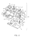
- FIG. 2 is an exploded perspective view of the optoelectronic transceiver module of FIG. 1, but viewed from another aspect;
- FIG. 3 is an exploded perspective view of the optoelectronic transceiver module of FIG. 1, but viewed from still another aspect; and
- FIG. 4 is an assembled view of the optoelectronic transceiver module of FIG. 1.
- Referring to FIG. 1, an
optoelectronic transceiver module 99 in accordance with the present invention has atop housing 1, abottom housing 2, achassis 3, areceptacle 4, aPCB 5 and anoptoelectronic subassembly 6. - The
receptacle 4 has the shape of an oblong box. Thereceptacle 4 comprises afront portion 43 and arear portion 44. The size of thefront portion 43 is large than that of therear portion 44. Thus arear face 431 is defined on thefront portion 43 around a periphery of a junction of the front andrear portions top housing 1. Referring also to FIG. 3, thefront portion 43 defines twoopenings receptacle 4. Rear portions of theopenings optoelectronic subassembly 6, and front portions of theopenings optoelectronic subassembly 6 comprises a transceiver. The transceiver comprises atransmitter 61 and areceiver 62. Thetransmitter 61 may typically be a laser diode (LD) or light emitting diode (LED), and thereceiver 62 may typically be a photo diode. A plurality ofconductive leads 605 extends from a rear of the transceiver, and is soldered to thePCB 5. Two T-shaped grooves 441 are defined in a bottom surface of therear portion 44 of thereceptacle 4, for engagement of thereceptacle 4 with thetop housing 1. A pair ofprotuberances 442 is formed on a top surface of thereceptacle 4. - Referring also to FIG. 2, the
PCB 5 has a narrowrear section 52 and awide front section 51. Threeposition holes 511 are defined through thePCB 5 in the vicinity of three edges thereof respectively. The conductive leads 605 of theoptoelectronic subassembly 6 are soldered to thefront section 51 of thePCB 5, to establish electrical contact between theoptoelectronic subassembly 6 and thePCB 5. Therear section 52 of thePCB 5 has a row ofelectrical contacts 520 at a rear end thereof, for electrical connection of thePCB 5 with an electrical connector (not shown). - The
chassis 3 may be made of metal, plastic or other suitable material. Thechassis 3 generally has the shape of an oblong box, for accommodating and protecting thePCB 5. Threepoles 313 depend from a bottom face of theplate 31 of thechassis 3. Threescrew holes 312 are defined in a top face of theplate 31 of thechassis 3 and through the threepoles 313 respectively, corresponding to the threeposition holes 511 of thePCB 5. A rear of thechassis 3 forms aseat 33. Asupport plate 330 extends forwardly from a bottom of theseat 33. Two screw holes 311 are defined in thechassis 3. Thechassis 3 has a pair of opposite side walls 32. Two spacedrecesses 320 are defined at a top edge of each side wall 32, for engagement of thechassis 3 with thebottom housing 2. A pair of depressions 321 (see FIG. 3) is defined in opposite sides of a rear end of thechassis 3. Three fastening components, such as screws 8 (only one shown), are for fixing thePCB 5 on thechassis 3. - The
bottom housing 2 is made of metal, and has a generally U-shaped configuration. Thebottom housing 2 has arectangular bottom wall 20, and twoside walls 21 extending perpendicularly upwardly from thebottom wall 20. Twoprotrusions 212 are inwardly formed at front and rear ends of a top of eachside wall 21, for engaging in therecesses 320 of thechassis 3. Aslot 213 is defined below eachprotrusion 212 of each side wall 32. Arectangular opening 211 is defined in eachside wall 21 below eachslot 213. Theslots 213 and therectangular openings 211 are for mating with thetop housing 1. - The
top housing 1 is made of metal, and has atop wall 11. Ashallow trough 110 is formed at a middle of thetop wall 11. Two annular flanges (not labeled) extend downwardly from thetrough 110. Two position holes 111 are respectively defined in the annular flanges, corresponding to the screw holes 311 of thechassis 3. A pair ofparallel grounding tabs 113 is formed near a front end of thetop wall 11 of thetop housing 1. A pair of parallelrectangular openings 112 is defined between the groundingtabs 113 and thetrough 110, corresponding to theprotuberances 442 of thereceptacle 4. A pair offorward side walls 14 depends from opposite sides of thetop wall 11 of thetop housing 1. A pair ofrearward side walls 12 depends from opposite sides of thetop wall 11 of thetop housing 1. Two pairs of lockingtabs 13 respectively depend from opposite sides of thetop wall 11 of thetop housing 1, between the forward andrearward side walls flap 142 is inwardly formed at a bottom of eachforward side wall 14, for engaging in the T-shape grooves 441 of thereceptacle 4. Eachforward side wall 14 has agrounding tab 113. A tab 121 (best seen in FIG.3) extends inwardly from a rear end of eachrearward side wall 12, for engaging in thedepressions 321 of thechassis 3. Each lockingtab 13 is a rectangular plate, the size of which corresponds to eachslot 213 of thebottom housing 2. Aspring tongue 131 is outwardly formed at a center of each lockingtab 13. A lower end of eachspring tongue 131 is integrally joined with thelocking tab 13, and an upper end of eachspring tongue 131 protrudes outwardly from the lockingtab 13. Two fastening components, such asscrews 7, are for attaching thetop housing 1 to thechassis 3. - Referring to FIG. 4, a
labeling tape 991 is for attachment to theoptoelectronic transceiver module 99 after assembly. - In assembly of the
optoelectronic transceiver module 99, thePCB 5 and thechassis 3 are firstly attached together. Therear section 52 of thePCB 5 is inserted into theseat 33 of thechassis 3. Thepoles 313 of thechassis 3 press down on thePCB 5, and thesupport plate 330 of thechassis 3 supports thePCB 5 by abutting against a bottom face thereof. Thescrews 8 are extended through the position holes 511 of thePCB 5 to threadedly engage in the screw holes 312 of thepoles 313. Thetop housing 1 is then attached to thereceptacle 4 and thechassis 3. Thescrews 7 are extended through the position holes 111 of thetop housing 1 to threadedly engage in the screw holes 311 of thechassis 3. Theprotuberances 442 of thereceptacle 4 are received in theopenings 112 of thetop housing 1. The T-shapedflaps 142 of thetop housing 1 are engaged in the T-shapedgrooves 441 of thereceptacle 4. Finally, thebottom housing 2 is attached to thechassis 3 and thetop housing 1. The lockingtabs 13 of thetop housing 1 are extended through theslots 213 of thebottom housing 2 until thespring tongues 131 of the lockingtabs 13 engage in theopenings 211 of thebottom housing 2. Theprotrusions 212 of thebottom housing 2 are engaged in therecesses 320 of thechassis 3. FIG. 4 shows the finally assembledoptoelectronic transceiver module 99. Thelabeling tape 991 is glued to thetrough 110 of thetop housing 1, to show some information about theoptoelectronic transceiver module 99 and to cover thescrews 7. - The
chassis 3 of theoptoelectronic transceiver module 99 is preferably made of metal. ThePCB 5 at the position holes 511 is coated with conductive material, and the conductive material is connected with a grounding circuit of thePCB 5. Thechassis 3 is thus electrically connected with the grounding circuit of thePCB 5 via thescrews 8 which engage with the conductive coating at the position holes 511. The top andbottom housings chassis 3. The optoelectronic transceiver module 9 thus effectively forms a grounding path between the grounding circuit of thePCB 5 and the top andbottom housings bottom housing - It should be understood that various changes and modifications to the presently preferred embodiment described herein will be apparent to those skilled in the art. Such changes and modifications may be made without departing from the spirit and scope of the present invention and without diminishing the present invention's advantages. Thus, it is intended that such changes and modifications be covered by the appended claims.
Claims (12)
Applications Claiming Priority (3)
| Application Number | Priority Date | Filing Date | Title |
|---|---|---|---|
| TW90209364 | 2001-06-06 | ||
| TW090209364U TW514344U (en) | 2001-06-06 | 2001-06-06 | Optoelectric transmitting and receiving module |
| TW90209364U | 2001-06-06 |
Publications (2)
| Publication Number | Publication Date |
|---|---|
| US20030000725A1 true US20030000725A1 (en) | 2003-01-02 |
| US6633420B2 US6633420B2 (en) | 2003-10-14 |
Family
ID=21684361
Family Applications (1)
| Application Number | Title | Priority Date | Filing Date |
|---|---|---|---|
| US09/939,159 Expired - Lifetime US6633420B2 (en) | 2001-06-06 | 2001-08-24 | Optoelectronic transceiver module |
Country Status (2)
| Country | Link |
|---|---|
| US (1) | US6633420B2 (en) |
| TW (1) | TW514344U (en) |
Cited By (2)
| Publication number | Priority date | Publication date | Assignee | Title |
|---|---|---|---|---|
| CN106443913A (en) * | 2016-12-20 | 2017-02-22 | 中航海信光电技术有限公司 | Optical module packaging structure and optical module |
| US9621216B1 (en) * | 2016-02-01 | 2017-04-11 | Nanning Fugui Precision Industrial Co., Ltd. | Cover and electronic device having same |
Families Citing this family (7)
| Publication number | Priority date | Publication date | Assignee | Title |
|---|---|---|---|---|
| US20030235375A1 (en) * | 2002-06-25 | 2003-12-25 | Kamath Kishore K. | Transceivers with improved cross talk |
| US20060110164A1 (en) * | 2004-11-19 | 2006-05-25 | Kirk Cook | Multiple PCBA transceiver |
| US7563035B2 (en) | 2005-04-29 | 2009-07-21 | Finisar Corporation | Connector for box optical subassembly |
| CN201741940U (en) | 2010-06-10 | 2011-02-09 | 富士康(昆山)电脑接插件有限公司 | Electric connector module |
| JP2014016395A (en) * | 2012-07-06 | 2014-01-30 | Sumitomo Electric Ind Ltd | Optical transceiver |
| CN104540076B (en) * | 2014-11-20 | 2018-09-07 | 歌尔股份有限公司 | Loud speaker module |
| US11177594B2 (en) * | 2020-04-09 | 2021-11-16 | Ii-Vi Delaware, Inc. | Housing for pluggable module |
Family Cites Families (5)
| Publication number | Priority date | Publication date | Assignee | Title |
|---|---|---|---|---|
| US4672685A (en) * | 1986-01-03 | 1987-06-09 | Motorola, Inc. | Dual band antenna having separate matched inputs for each band |
| US5312160A (en) * | 1991-11-12 | 1994-05-17 | Larry A. Davis | Vehicle seat mounted headrest and utility console |
| US5528408A (en) * | 1994-10-12 | 1996-06-18 | Methode Electronics, Inc. | Small footprint optoelectronic transceiver with laser |
| JPH08248277A (en) * | 1995-01-09 | 1996-09-27 | Fujitsu Ltd | Optical device |
| US6024500A (en) * | 1998-04-29 | 2000-02-15 | Lucent Technologies Inc. | Transceiver package |
-
2001
- 2001-06-06 TW TW090209364U patent/TW514344U/en not_active IP Right Cessation
- 2001-08-24 US US09/939,159 patent/US6633420B2/en not_active Expired - Lifetime
Cited By (2)
| Publication number | Priority date | Publication date | Assignee | Title |
|---|---|---|---|---|
| US9621216B1 (en) * | 2016-02-01 | 2017-04-11 | Nanning Fugui Precision Industrial Co., Ltd. | Cover and electronic device having same |
| CN106443913A (en) * | 2016-12-20 | 2017-02-22 | 中航海信光电技术有限公司 | Optical module packaging structure and optical module |
Also Published As
| Publication number | Publication date |
|---|---|
| US6633420B2 (en) | 2003-10-14 |
| TW514344U (en) | 2002-12-11 |
Similar Documents
| Publication | Publication Date | Title |
|---|---|---|
| US6830383B2 (en) | Small form factor pluggable optoelectronic transceiver module | |
| US6483711B1 (en) | Optoelectronic transceiver module with additional grounding | |
| US6530785B1 (en) | Packing means for small form-factor module | |
| US6556446B1 (en) | Optoelectronic transceiver module assembly | |
| US6434015B1 (en) | Small form-factor pluggable module having release device | |
| US6368153B1 (en) | Small form-factor pluggable transceiver cage | |
| EP0117022B1 (en) | Fiber optic connector assembly | |
| US6508670B1 (en) | Small form-factor pluggable transceiver cage | |
| EP1726978B1 (en) | Photoelectric combined connector | |
| US6341899B1 (en) | Hybrid connector | |
| EP0442608B1 (en) | Transceiver package | |
| US6319062B1 (en) | Board mounted electrical connector | |
| US4547039A (en) | Housing mountable on printed circuit board to interconnect fiber optic connectors | |
| US6174194B1 (en) | Add-on electrical assembly with light transmission means | |
| US6729905B1 (en) | Transceiver cage assembly | |
| USRE36820E (en) | Removable optoelectronic module | |
| US6580614B2 (en) | Optical transceiver module with metallic latches | |
| US6893168B2 (en) | Optical transceiver module with multiple grounding paths | |
| US6633420B2 (en) | Optoelectronic transceiver module | |
| GB2479049A (en) | Optical transceiver module | |
| US7090410B2 (en) | Optical receptacle with low transmission loss and photoelectric conversion module for the same | |
| US7207730B2 (en) | Small form factor transceiver | |
| US6863451B2 (en) | Optical module | |
| JP7099993B2 (en) | connector | |
| US20030081907A1 (en) | Device for blocking emitted light |
Legal Events
| Date | Code | Title | Description |
|---|---|---|---|
| AS | Assignment |
Owner name: HON HAI PRECISION IND. CO., LTD., TAIWAN Free format text: ASSIGNMENT OF ASSIGNORS INTEREST;ASSIGNOR:HUANG, NAN TSUNG;REEL/FRAME:012128/0900 Effective date: 20010725 |
|
| STCF | Information on status: patent grant |
Free format text: PATENTED CASE |
|
| FPAY | Fee payment |
Year of fee payment: 4 |
|
| FPAY | Fee payment |
Year of fee payment: 8 |
|
| AS | Assignment |
Owner name: GOOGLE INC., CALIFORNIA Free format text: ASSIGNMENT OF ASSIGNORS INTEREST;ASSIGNORS:HON HAI PRECISION INDUSTRY CO., LTD;GOLD CHARM LIMITED;HONG FUJIN PRECISION INDUSTRIAL (SHENZHEN) CO.;REEL/FRAME:032743/0832 Effective date: 20140228 |
|
| FPAY | Fee payment |
Year of fee payment: 12 |
|
| AS | Assignment |
Owner name: GOOGLE LLC, CALIFORNIA Free format text: CHANGE OF NAME;ASSIGNOR:GOOGLE INC.;REEL/FRAME:044127/0735 Effective date: 20170929 |