US20140028107A1 - Apparatus and method for wirelessly receiving power - Google Patents
Apparatus and method for wirelessly receiving power Download PDFInfo
- Publication number
- US20140028107A1 US20140028107A1 US13/940,695 US201313940695A US2014028107A1 US 20140028107 A1 US20140028107 A1 US 20140028107A1 US 201313940695 A US201313940695 A US 201313940695A US 2014028107 A1 US2014028107 A1 US 2014028107A1
- Authority
- US
- United States
- Prior art keywords
- target resonator
- capacitor
- switch unit
- wireless power
- resonator
- Prior art date
- Legal status (The legal status is an assumption and is not a legal conclusion. Google has not performed a legal analysis and makes no representation as to the accuracy of the status listed.)
- Granted
Links
Images




Classifications
-
- H—ELECTRICITY
- H02—GENERATION; CONVERSION OR DISTRIBUTION OF ELECTRIC POWER
- H02J—ELECTRIC POWER NETWORKS; CIRCUIT ARRANGEMENTS OR SYSTEMS FOR SUPPLYING OR DISTRIBUTING ELECTRIC POWER; SYSTEMS FOR STORING ELECTRIC ENERGY
- H02J50/00—Circuit arrangements or systems for wireless supply or distribution of electric power
- H02J50/10—Circuit arrangements or systems for wireless supply or distribution of electric power using inductive coupling
- H02J50/12—Circuit arrangements or systems for wireless supply or distribution of electric power using inductive coupling of the resonant type
-
- H—ELECTRICITY
- H01—ELECTRIC ELEMENTS
- H01F—MAGNETS; INDUCTANCES; TRANSFORMERS; SELECTION OF MATERIALS FOR THEIR MAGNETIC PROPERTIES
- H01F38/00—Adaptations of transformers or inductances for specific applications or functions
- H01F38/14—Inductive couplings
-
- H—ELECTRICITY
- H02—GENERATION; CONVERSION OR DISTRIBUTION OF ELECTRIC POWER
- H02J—ELECTRIC POWER NETWORKS; CIRCUIT ARRANGEMENTS OR SYSTEMS FOR SUPPLYING OR DISTRIBUTING ELECTRIC POWER; SYSTEMS FOR STORING ELECTRIC ENERGY
- H02J50/00—Circuit arrangements or systems for wireless supply or distribution of electric power
- H02J50/005—Mechanical details of housing or structure aiming to accommodate the power transfer means, e.g. mechanical integration of coils, antennas or transducers into emitting or receiving devices
-
- H—ELECTRICITY
- H02—GENERATION; CONVERSION OR DISTRIBUTION OF ELECTRIC POWER
- H02J—ELECTRIC POWER NETWORKS; CIRCUIT ARRANGEMENTS OR SYSTEMS FOR SUPPLYING OR DISTRIBUTING ELECTRIC POWER; SYSTEMS FOR STORING ELECTRIC ENERGY
- H02J50/00—Circuit arrangements or systems for wireless supply or distribution of electric power
- H02J50/40—Circuit arrangements or systems for wireless supply or distribution of electric power using two or more transmitting or receiving devices
-
- H—ELECTRICITY
- H02—GENERATION; CONVERSION OR DISTRIBUTION OF ELECTRIC POWER
- H02J—ELECTRIC POWER NETWORKS; CIRCUIT ARRANGEMENTS OR SYSTEMS FOR SUPPLYING OR DISTRIBUTING ELECTRIC POWER; SYSTEMS FOR STORING ELECTRIC ENERGY
- H02J50/00—Circuit arrangements or systems for wireless supply or distribution of electric power
- H02J50/80—Circuit arrangements or systems for wireless supply or distribution of electric power involving the exchange of data, concerning supply or distribution of electric power, between transmitting devices and receiving devices
-
- H—ELECTRICITY
- H04—ELECTRIC COMMUNICATION TECHNIQUE
- H04B—TRANSMISSION
- H04B5/00—Near-field transmission systems, e.g. inductive or capacitive transmission systems
- H04B5/70—Near-field transmission systems, e.g. inductive or capacitive transmission systems specially adapted for specific purposes
- H04B5/79—Near-field transmission systems, e.g. inductive or capacitive transmission systems specially adapted for specific purposes for data transfer in combination with power transfer
-
- H—ELECTRICITY
- H02—GENERATION; CONVERSION OR DISTRIBUTION OF ELECTRIC POWER
- H02J—ELECTRIC POWER NETWORKS; CIRCUIT ARRANGEMENTS OR SYSTEMS FOR SUPPLYING OR DISTRIBUTING ELECTRIC POWER; SYSTEMS FOR STORING ELECTRIC ENERGY
- H02J7/00—Circuit arrangements for charging or discharging batteries or for supplying loads from batteries
-
- H—ELECTRICITY
- H02—GENERATION; CONVERSION OR DISTRIBUTION OF ELECTRIC POWER
- H02J—ELECTRIC POWER NETWORKS; CIRCUIT ARRANGEMENTS OR SYSTEMS FOR SUPPLYING OR DISTRIBUTING ELECTRIC POWER; SYSTEMS FOR STORING ELECTRIC ENERGY
- H02J7/00—Circuit arrangements for charging or discharging batteries or for supplying loads from batteries
- H02J7/90—Regulation of charging or discharging current or voltage
- H02J7/933—Regulation of charging or discharging current or voltage the cycle being controlled or terminated in response to electric parameters
Definitions
- the following description relates to an apparatus and method for wirelessly receiving power.
- the near-field wireless power transmission refers to an example in which a distance between a transmission coil and a reception coil is sufficiently short, compared to a wavelength in an operation frequency.
- a wireless power transmission and reception system using a resonance characteristic may include a source device configured to supply power, and a target device configured to receive the supplied power.
- a wireless power receiver includes a receiving unit configured to wirelessly receive power through a resonance between a source resonator and a target resonator.
- the wireless power receiver further includes a control unit configured to connect the target resonator to at least one capacitor to control a range of a voltage output from the target resonator.
- a wireless power receiver in another general aspect, includes a receiving unit configured to wirelessly receive power through a resonance between a source resonator and a target resonator.
- the wireless power receiver further includes a control unit configured to connect the target resonator to a passive device to control a range of a voltage output from the target resonator.
- a wireless power reception method includes wirelessly receiving power through a resonance between a source resonator and a target resonator.
- the wireless power reception method further includes connecting the target resonator to at least one capacitor to control a range of a voltage output from the target resonator.
- FIG. 1 is a diagram illustrating an example of an equivalent circuit of a wireless power transmission system.
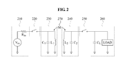
- FIG. 2 is a diagram illustrating another example of an equivalent circuit of a wireless power transmission system.
- FIGS. 3A through 3E are diagrams illustrating an example of a wireless power receiver, and examples of waveforms of voltages measured at a rear end of a target resonator when a passive device is not connected to the target resonator in the wireless power receiver.
- FIG. 4 is a block diagram illustrating an example of a wireless power receiver.
- FIGS. 5A through 10C are diagrams illustrating examples of configurations and operations of wireless power receivers.
- FIG. 11 is a flowchart illustrating an example of a wireless power reception method.
- a wireless power transmission system may be applied to various systems requiring wireless power.
- the wireless power transmission system may be used in a system enabling use of wireless power, for example, a mobile phone, a wireless television (TV), and/or other systems known to one of ordinary skill in the art. Additionally, the wireless power transmission system may be applicable in a bio-healthcare field, and may be used to remotely transmit power to a device inserted into a human body, or used to wirelessly transmit power to a bandage-shaped device for measurement of a heart rate.
- the wireless power transmission system may be used to remotely control an information storage device without a power source.
- the wireless power transmission system may be applied to a system configured to supply power to an information storage device to remotely operate the information storage device, and to wirelessly request information stored in the information storage device.
- the wireless power transmission system may receive energy supplied from a power supply unit, and may store the energy in a source resonator, to generate a signal.
- the wireless power transmission system may induce the source resonator to self-resonate by powering off a switch that electrically connects the power supply unit to the source resonator.
- a target resonator with the same resonant frequency as the self-resonating source resonator is disposed within a distance close enough to resonate with the source resonator, a mutual resonance phenomenon may occur between the source resonator and the target resonator.
- the source resonator may refer to a resonator that receives energy from a power supply unit
- the target resonator may refer to a resonator that receives energy from the source resonator due to the mutual resonance phenomenon
- FIG. 1 illustrates an example of an equivalent circuit of a wireless power transmission system.
- the wireless power transmission system includes a source-target structure including a source device and a target device.
- the wireless power transmission system includes a wireless power transmitter corresponding to the source device, and a wireless power receiver corresponding to the target device.
- the wireless power transmitter includes a power input unit 110 , a power transmitting unit 120 , a switch unit 130 , and a capacitor C 1 .
- the power input unit 110 is physically-separated from the power transmitting unit 120 by the switch unit 130 and the capacitor C 1 .
- the wireless power receiver includes a receiving unit 140 , a power output unit 150 , a switch unit 160 , and a capacitor C 2 .
- the receiving unit 140 is physically-separated from the power output unit 150 by the switch unit 160 and the capacitor C 2 .
- the power input unit 110 stores energy in the capacitor C 1 , using a power supply unit generating an input voltage V DC .
- the switch unit 130 connects the capacitor C 1 to the power input unit 110 , while the energy is transmitted from the power supply unit and stored in the capacitor C 1 . To discharge the stored energy, the switch unit 130 disconnects the capacitor C 1 from the power input unit 110 , and connects the capacitor C 1 to the power transmitting unit 120 . The switch unit 130 prevents the capacitor C 1 from being connected to the power input unit 110 and the power transmitting unit 120 at the same time.
- the power transmitting unit 120 transfers electromagnetic energy to the receiving unit 140 , through mutual resonance.
- the power transmitting unit 120 transfers the electromagnetic energy through the mutual resonance between a transmission coil L 1 of the power transmitting unit 120 and a reception coil L 2 of the receiving unit 140 .
- the level of the mutual resonance between the transmission coil L 1 and the reception coil L 2 is affected by mutual inductance M between the transmission coil L 1 and the reception coil L 2 .
- the power transmitting unit 120 may quantize the electromagnetic energy stored in the capacitor C 1 , and may transmit the quantized energy to the receiving unit 140 for a symbol unit.
- the power transmitting unit 120 may control different amounts of the electromagnetic energy to be transmitted to the receiving unit 140 for each symbol unit, and may also transmit information to the receiving unit 140 .
- the symbol unit may be used to transfer the information in a single bit between the source device and the target device.
- the symbol unit refers to a period or cycle during which the charged capacitor C 1 is discharged through the mutual resonance between a source resonator (e.g., the power transmitting unit 120 ) and a target resonator (e.g., the receiving unit 140 ), based on an operation of the switch unit 130 .
- the power input unit 110 includes the power supply unit generating the input voltage V DC , an internal resistor R in , and the capacitor C 1
- the power transmitting unit 120 includes a resistor R 1 , the transmission coil L 1 , and the capacitor C 1 that form the source resonator.
- the switch unit 130 includes at least one switch.
- the switch may include an active element enabling an on/off function.
- R 1 , L 1 , and C 1 represent a resistance, an inductance, and a capacitance, respectively, of the source resonator.
- a voltage applied to the capacitor C 1 among the input voltage V DC is represented by V in .
- the receiving unit 140 receives the electromagnetic energy from the power transmitting unit 120 , and stores the received electromagnetic energy in the capacitor C 2 .
- the switch unit 160 connects the capacitor C 2 to the receiving unit 140 , while the electromagnetic energy is transmitted from the power transmitting unit 120 and stored in the capacitor C 2 .
- the switch unit 160 disconnects the capacitor C 2 from the receiving unit 140 , and connects the capacitor C 2 to the power output unit 150 .
- the power output unit 150 transfers the energy stored in the capacitor C 2 to a load, for example, a battery.
- the switch unit 160 prevents the capacitor C 2 from being connected to the receiving unit 140 and the power output unit 150 at the same time.
- the receiving unit 140 receives the electromagnetic energy through the mutual resonance between the reception coil L 2 of the receiving unit 140 and the transmission coil L 1 of the power transmitting unit 120 .
- the receiving unit 140 charges the capacitor C 2 connected to the reception coil L 2 , with the received electromagnetic energy.
- the power output unit 150 transfers the energy used to charge the capacitor C 2 to the load, for example, the battery.
- the power output unit 150 may transfer the energy to a target device requiring power, instead of to the battery.
- the receiving unit 140 may receive the electromagnetic energy from the power transmitting unit 120 for a symbol unit.
- the receiving unit 140 may further receive the information from the power transmitting unit 120 , and may demodulate the information based on an amount of the received electromagnetic energy.
- the receiving unit 140 includes a resistor R 2 , the reception coil L 2 , and the capacitor C 2 that form a target resonator, and the power output unit 150 includes the capacitor C 2 and the battery.
- the switch unit 160 includes at least one switch.
- R 2 , L 2 , and C 2 represent a resistance, an inductance, and a capacitance, respectively, of the target resonator.
- a voltage applied to the capacitor C 2 among the electromagnetic energy received by the reception coil L 2 is represented by V out .
- the above-described wireless power transmission system enables power to be wirelessly transmitted when the power input unit 110 is physically separated from the power transmitting unit 120 , and the receiving unit 140 is physically separated from the power output unit 150 .
- This wireless power transmission system is referred to as a Resonator Isolation (RI) system.
- the RI system does not need a power amplifier because power may be supplied from a direct current (DC) source (e.g., the power supply unit generating the input voltage V DC ) directly to the source resonator. Further, the RI system does not require a rectifying operation of a rectifier because energy is captured from energy used to charge the capacitor C 2 of the wireless power receiver. Further, a transmission efficiency is not sensitive to a change in a distance between the wireless power transmitter and the wireless power receiver because there is no need to perform impedance matching. Additionally, the RI system may be easily extended from the wireless power transmission system including a single transmitter and a single receiver to a wireless power transmission system including a plurality of transmitters and a plurality of receivers.
- DC direct current
- FIG. 2 illustrates another example of an equivalent circuit of a wireless power transmission system.
- FIG. 2 illustrates another example of an RI system.
- the wireless power transmission system includes a source-target structure including a source device and a target device.
- the wireless power transmission system includes a wireless power transmitter corresponding to the source device, and a wireless power receiver corresponding to the target device.
- the wireless power transmitter includes a power charging unit 210 , a control unit 220 , and a transmitting unit 230 .
- the power charging unit 210 is physically separated from the transmitting unit 230 by the control unit 220 .
- the wireless power receiver includes a charging unit 240 , a control unit 250 , and a power output unit 260 .
- the charging unit 240 is physically separated from the power output unit 260 by the control unit 250 .
- the power charging unit 210 includes a power supply unit V in and an internal resistor R in .
- the transmitting unit 230 includes a capacitor C 1 and an inductor L 1 .
- the capacitor C 1 and the inductor L 1 are referred to as a source resonator.
- the source resonator functions as the transmitting unit 230 .
- the transmitting unit 230 transmits energy stored in the source resonator to a target resonator, through mutual resonance M 270 between the source resonator and the target resonator.
- the control unit 220 includes a switch, and turns on (e.g., closes) the switch to enable power to be supplied from the power charging unit 210 to the transmitting unit 230 .
- a voltage from the power supply unit V in is applied to the capacitor C 1
- a current is applied to the inductor L 1 .
- the voltage applied to the capacitor C 1 may include a value of ‘0’
- the current flowing in the inductor L 1 may include a value of ‘V in /R in ’.
- the source resonator may be charged with power, using the current applied to the inductor L 1 .
- the control unit 220 turns off (e.g., opens) the switch.
- the control unit 220 may set information on the predetermined value.
- the control unit 220 separates the power charging unit 210 from the transmitting unit 230 .
- the source resonator starts self-resonating between the capacitor C 1 and the inductor L 1 .
- Energy stored in the source resonator is transferred to the target resonator, through the mutual resonance M 270 between the source resonator and the target resonator.
- a resonant frequency f 1 of the source resonator may be the same as a resonant frequency f 2 of the target resonator. Additionally, a value of the resonant frequency f 1 , and a value of resonant frequency f 2 , may be determined based on the following equations.
- L 1 denotes an inductance of the inductor L 1
- C 1 denotes a capacitance of the capacitor C 1
- L 2 denotes an inductance of an inductor L 2 of the target resonator
- C 2 denotes a capacitance of a capacitor C 2 of the target resonator.
- the transmitting unit 230 may quantize the energy stored in the source resonator, and may transmit the quantized energy to the target resonator for a symbol unit. For example, the transmitting unit 230 may control different amounts of the energy to be transmitted to the target resonator for each symbol unit, and may also transmit information to the target resonator.
- the symbol unit may be used to transfer the information in a single bit between the source device and the target device.
- the symbol unit refers to a period or cycle during which the charged capacitor C 1 and the inductor L 1 are discharged through the mutual resonance M 270 between the source resonator and target resonator, based on an operation of the control unit 220 .
- the charging unit 240 includes the capacitor C 2 and the inductor L 2 .
- the capacitor C 2 and the inductor L 2 are referred to as the target resonator.
- the target resonator functions as the charging unit 240 .
- the charging unit 240 receives the energy stored in the source resonator via the target resonator, through the mutual resonance M 270 between the source resonator and the target resonator.
- the power output unit 260 includes a load and a capacitor C L .
- the control unit 250 includes a switch, and turns off (e.g., opens) the switch. By turning off the switch, the control unit 250 separates the charging unit 240 from the power output unit 260 .
- the source resonator is separated from the power supply unit V in by the control unit 220 including the switch being open, and the target resonator is separated from the load and the capacitor C L by the control unit 250 including the switch being open.
- the energy stored in the source resonator is transferred to the target resonator, through the mutual resonance M 270 .
- the energy stored in the source resonator charges the capacitor C 2 and the inductor L 2 of the charging unit 240 , through the mutual resonance M 270 .
- the resonant frequency f 1 of the source resonator may be the same as the resonant frequency f 2 of the target resonator.
- the control unit 250 When the energy used to charge the target resonator reaches a predetermined value or a maximum value, the control unit 250 turns on (e.g., closes) the switch. The control unit 250 may set information on the predetermined value. By turning on the switch, the control unit 250 connects the capacitor C L to the charging unit 240 , and the resonant frequency of the target resonator is changed. A value of the changed resonant frequency f′ 2 of the target resonator may be determined based on the following equation.
- Equation (2) C L denotes a capacitance of the capacitor C L .
- the mutual resonance M 270 between the source resonator and the target resonator is terminated.
- the mutual resonance M 270 is removed.
- the charging unit 240 transfers power used to charge the capacitor C 2 and the inductor L 2 to the power output unit 260 , which transfers the power to a load.
- the control unit 250 turns off the switch.
- the charging unit 240 may recharge the target resonator with energy using the mutual resonance M 270 between the source resonator and the target resonator.
- the charging unit 240 may receive the energy from the transmitting unit 230 for a symbol unit.
- the charging unit 240 may also receive the information from the transmitting unit 230 , and may demodulate the information based on an amount of the received energy.
- the switch of the control unit 250 is not connected between the charging unit 240 and the power output unit 260 . Accordingly, it is possible to prevent transmission efficiency from being reduced due to a connection to the switch.
- a scheme of controlling a point in time of capturing energy stored in a target resonator of FIG. 2 may be performed more easily than a scheme of transferring energy stored in a capacitor of FIG. 1 .
- the scheme of transferring the energy stored in a capacitor only the energy in the capacitor is captured.
- the energy stored in an inductor and a capacitor of the target resonator is captured. Accordingly, a degree of freedom for the point in time of capturing the energy may be improved.
- a transmitter in an RI system may repeatedly charge a source resonator with energy and discharge energy through a connection to a switch.
- a single charge and discharge of energy may be referred as a single symbol.
- a receiver in the RI system may operate a switch of the receiver based on an operation period of a switch of the transmitter that repeatedly performs charging and discharging.
- the receiver may need to know when the switch of the transmitter is powered off, when the switch of the transmitter is powered on, when a mutual resonance is started, and when energy stored in the target resonator includes a peak value.
- An method of acquiring information regarding an on/off time of the switch of the transmitter, and matching an on/off time of the switch of the receiver to the acquired information, may be referred as a time synchronization.
- FIGS. 3A through 3E illustrate an example of a wireless power receiver, and examples of waveforms of voltages measured at a rear end of a target resonator when a passive device is not connected to the target resonator in the wireless power receiver.
- the wireless power receiver includes the target resonator, including an inductor L 2 and a capacitor C 2 , a switch connected to the rear end of the target resonator, a capacitor C L , a rectifier, a regulator, a battery, a Low-Drop Output (LDO) regulator, and a digital chip.
- LDO Low-Drop Output
- the capacitor C L When the switch is powered on, the capacitor C L is connected to the target resonator, and a resonant frequency of the target resonator is changed. Accordingly, a resonant frequency of a source resonator of a wireless power transmitter is no longer matched to the resonant frequency of the target resonator, and a mutual resonance between the source resonator and the target resonator is terminated.
- power stored in the target resonator is transferred to the battery through the rectifier and the regulator; that is, the battery is charged.
- the rectifier rectifies an AC signal of the power to a DC signal
- the regulator steps up or steps down the rectified voltage to a voltage needed by the battery.
- Power stored in the battery is transferred to the digital chip through the LDO regulator.
- the LDO regulator steps down an output voltage of the battery to a voltage needed by the digital chip.
- a waveform (e.g., an AC signal) of a voltage measured at an input end 310 of the rectifier is shown.
- the waveform of the voltage may include, for example, a dynamic range 360 or 370 . That is, based on a channel characteristic between the source resonator and the target resonator, an amplitude of a signal received by the target resonator may be changed by a large width. When a distance between the source resonator and the target resonator is decreased, an amount of power transferred from the source resonator to the target resonator may be increased, and the amplitude of the signal received by the target resonator may be increased.
- the amount of the power transferred from the source resonator to the target resonator may be decreased, and the amplitude of the signal received by the target resonator may be decreased.
- FIGS. 3A and 3C a waveform of a voltage measured at an output end 320 of the rectifier is shown.
- the waveform of the voltage indicates a signal that is full bridge rectified by the rectifier.
- the regulator generates a voltage suitable for a rated voltage of the battery. For example, if the rated voltage of the battery is set to 3.3 V, the regulator generates a DC signal of 3.3 V from the rectified signal to be input to the battery.
- the regulator may include a booster converter configured to step up an input voltage, and/or a buck converter configured to step down the input voltage. Additionally, the battery outputs a voltage of 3.3 V at the output end 340 .
- FIGS. 3A and 3E a waveform of a voltage measured at an output end 350 of the LDO regulator is shown.
- the LDO regulator steps down the voltage output from the battery to the voltage needed by the digital chip. For example, if the digital chip needs a voltage of 1.8 V, the LDO regulator steps down the voltage of 3.3 V output from the battery to 1.8 V to be input to the digital chip.
- the dynamic range 360 may be changed to the dynamic range 370 , or vice versa.
- a variation in a dynamic range for example, a variation from the dynamic range 360 to the dynamic range 370 , or a variation from the dynamic range 370 to the dynamic range 360 , increases, an operation efficiency of the regulator and a charging efficiency of the battery may decrease.
- the operation efficiency of the regulator and the charging efficiency of the battery may increase.
- FIG. 4 illustrates an example of a wireless power receiver.
- the wireless power receiver includes a receiving unit 410 and a control unit 420 .
- the control unit 420 includes a timing controller 421 .
- the receiving unit 410 wirelessly receives power through a mutual resonance between a source resonator of a wireless power transmitter and a target resonator of the wireless power receiver.
- the receiving unit 410 may include the target resonator.
- the control unit 420 connects the target resonator to a passive device (e.g., one or more capacitors) to control a dynamic range of a voltage output from the target resonator.
- the voltage output from the target resonator may be applied to a rectifier. Accordingly, the control unit 420 controls a dynamic range of a voltage input to the rectifier, using the passive device.
- the passive device may include, for example, a first capacitor and a second capacitor.
- the first capacitor may include a capacitance greater than or equal to a capacitance of a capacitor included in the target resonator
- the second capacitor may include a capacitance less than the capacitance of the capacitor included in the target resonator.
- control unit 420 may connect the target resonator to the first capacitor and/or the second capacitor, to change a resonant frequency of the target resonator, and to attenuate the dynamic range of the voltage output from the target resonator.
- the target resonator may be connected in parallel to the first capacitor and/or the second capacitor. If the target resonator is connected to the first capacitor, power stored in the target resonator may be transferred to the first capacitor. Accordingly, the dynamic range of the voltage output from the target resonator may be attenuated in proportion to the capacitance of the first capacitor. In other words, an amplitude of a waveform of the voltage output from the target resonator may be decreased.
- the power stored in the target resonator may be transferred to the second capacitor, and accordingly, the dynamic range of the voltage output from the target resonator may be attenuated in proportion to the capacitance of the second capacitor.
- control unit 420 may connect the target resonator to the second capacitor, to change the resonant frequency of the target resonator, and to amplify the dynamic range of the voltage output from the target resonator.
- the target resonator includes an inductor and a capacitor. The control unit 420 may disconnect the capacitor of the target resonator from the inductor of the target resonator, and may connect the inductor to the second capacitor in parallel. The amplitude of the waveform of the voltage output from the target resonator may increase in proportion to a difference between the capacitance of the second capacitor and the capacitance of the capacitor in the target resonator.
- control unit 420 may connect the target resonator to the first capacitor and the second capacitor during the mutual resonance. If the target resonator is connected in parallel to the first capacitor and the second capacitor during the mutual resonance, a capacitance of the wireless power receiver may be increased. Accordingly, the amplitude of the waveform of the voltage output from the target resonator may be decreased, and a period of the waveform of the output voltage may be lengthened. If a voltage of the capacitor in the target resonator becomes less than or equal to a predetermined value, the capacitor in the target resonator may be disconnected from the inductor in the target resonator.
- the predetermined value may be set to, for example, 0 V.
- the control unit 420 may disconnect the capacitor in the target resonator from the inductor in the target resonator at a time at which the voltage of the capacitor in the target resonator includes a minimum value. Subsequently, the control unit 420 may disconnect the target resonator from the first capacitor, and may connect the target resonator to a load to capture the power stored in the target resonator in the load.
- the control unit 420 may be connected to the rectifier and a regulator. If a voltage greater than an output voltage of the control unit 420 is needed as an input voltage of the regulator, the control unit 420 may connect the second capacitor to the target resonator, and disconnect the capacitor of the target resonator from the inductor of the target resonator, to amplify an amplitude of the output voltage. If a voltage less than the output voltage of the control unit 420 is needed as the input voltage of the regulator, the control unit 420 may connect the first capacitor and/or the second capacitor to the target resonator to attenuate the amplitude of the output voltage.
- the timing controller 421 controls a timing in which the first capacitor and/or the second capacitor are connected to the target resonator. For example, if the power stored in the target resonator is greater than or equal to a predetermined value, the timing controller 421 may connect the target resonator to the first capacitor.
- the predetermined value may be a maximum value of the power to be stored in the target resonator.
- the timing controller 421 controls a timing in which the second capacitor is connected to the target resonator, and the capacitor of the target resonator is disconnected from the inductor of the target resonator. As the amplitude of the voltage output from the target resonator increases, the dynamic range of the voltage output from the target resonator becomes wider.
- the control unit 420 may control an overall operation of the wireless power receiver of FIG. 4 , and may perform a function of the receiving unit 410 .
- the receiving unit 410 and the control unit 420 are separately illustrated in FIG. 4 to separately describe each function.
- the control unit 420 may perform all functions, or may perform a portion of the functions.
- FIGS. 5A through 10C illustrate examples of configurations and operations of wireless power receivers.
- FIG. 5A illustrates an example of a configuration of a wireless power receiver configured to attenuate an amplitude of a signal input to a rectifier
- FIG. 5B illustrates an example of a change in the amplitude of the signal input to the rectifier based on an operation of a second switch unit 530 of FIG. 5A .
- the wireless power receiver includes a target resonator 510 , a first switch unit 520 , the second switch unit 530 , and a control unit 540 . Additionally, the wireless power receiver includes the rectifier, a regulator, a battery, and/or other elements located at a rear end of the second switch unit 530 and known to one of ordinary skill in the art. The wireless power receiver attenuates an amplitude of a signal output from the target resonator 510 .
- the target resonator 510 includes an inductor L 2 and a capacitor C 2 .
- the first switch unit 520 connects the target resonator 510 to the rectifier.
- the second switch unit 530 connects a capacitor C L to the target resonator 510 in parallel between the target resonator 510 and the rectifier.
- a capacitance of the capacitor C L may be equal to, greater than, or less than a capacitance of the capacitor C 2 .
- the control unit 540 controls an operation of the first switch unit 520 and an operation of the second switch unit 530 .
- the amplitude of the signal input to the rectifier may be decreased.
- a width of the decreased amplitude may be adjusted based on the capacitance of the capacitor C L .
- a mutual resonance between the target resonator 510 and a source resonator of a wireless power transmitter occurs.
- the target resonator 510 is connected to the rectifier, and power stored in the target resonator 510 is transferred to the battery through the rectifier and the regulator.
- the wireless power receiver performs charging of the battery.
- the second switch unit 530 is maintained in the off state, a signal output from the target resonator 510 is transferred to the rectifier without a change. If the second switch unit 530 is powered on at a time 550 , a portion of the power stored in the target resonator 510 charges the capacitor C L , and accordingly, the amplitude of the signal input to the rectifier is decreased.
- FIG. 6A illustrates an example of a configuration of a wireless power receiver configured to attenuate an amplitude of a signal input to a rectifier in various widths.
- FIGS. 6B through 6D illustrate examples of a change in the amplitude of the signal input to the rectifier based on operations of a second switch unit 630 and a third switch unit 640 of FIG. 6A .
- the wireless power receiver includes a target resonator 610 , a first switch unit 620 , the second switch unit 630 , the third switch unit 640 , and a control unit 650 .
- the wireless power receiver further includes the rectifier, a regulator, a battery, and/or other elements located at a rear end of the third switch unit 640 and known to one of ordinary skill in the art.
- the wireless power receiver attenuates an amplitude of an amplitude of a signal output from the target resonator 610 in various widths.
- the target resonator 610 includes an inductor L 2 and a capacitor C 2 .
- the first switch unit 620 connects the target resonator 610 to the rectifier.
- the second switch unit 630 connects a capacitor C L1 to the target resonator 610 in parallel between the target resonator 610 and the rectifier.
- a capacitance of the capacitor C L1 may be equal to, greater than, or less than a capacitance of the capacitor C 2 .
- the third switch unit 640 connects a capacitor C Ln to the target resonator 610 in parallel between the capacitor C L1 and the rectifier.
- a capacitance of the capacitor C Ln may be equal to, greater than, or less than the capacitance of the capacitor C L1 .
- the control unit 650 controls an operation of each of the first switch unit 620 , the second switch unit 630 and the third switch unit 640 .
- the second switch unit 630 When the second switch unit 630 is in an on state, and when the first switch unit 620 is powered on, a portion of power needed to be input to the rectifier is distributed to the capacitor C L1 , and accordingly, the amplitude of the signal input to the rectifier is decreased.
- the first switch unit 620 When each of the second switch unit 630 and the third switch unit 640 are in the on state, and when the first switch unit 620 is powered on, a portion of the power needed to be input to the rectifier is distributed to the capacitors C L1 and C Ln , and accordingly, the amplitude of the signal input to the rectifier is further decreased.
- the amplitude of the signal input to the rectifier may be adjusted based on a number of connected capacitors, e.g., the capacitances of the capacitors C L1 and C Ln .
- a mutual resonance between the target resonator 610 and a source resonator of a wireless power transmitter occurs.
- the target resonator 610 is connected to the rectifier, and power stored in the target resonator 610 is transferred to the battery through the rectifier and the regulator.
- the second switch unit 630 and the third switch unit 640 are maintained in the off state, the signal output from the target resonator 610 is transferred to the rectifier without a change, as shown in FIG. 6B .
- a portion of the power stored in the target resonator 610 charges the capacitor C L1 . Accordingly, the amplitude of the signal input to the rectifier is decreased by a width 660 .
- the amplitude of the signal input to the rectifier is decreased by a width 670 .
- the amplitude of the signal input to the rectifier is decreased based on a capacitance of one or more capacitors connected in parallel to the target resonator 610 , or based on a number of the capacitors.
- a wireless power receiver includes a target resonator 710 , a first switch unit 720 , a second switch unit 730 , and a third switch unit 740 .
- the wireless power receiver further includes a rectifier, a regulator, a battery, and/or other elements located at a rear end of the third switch unit 740 and known to one of ordinary skill in the art.
- the third switch unit 740 that connects the target resonator 710 and the rectifier is located at a rear end of the second switch unit 730 and a capacitor C Ln .
- the third switch unit 740 is connected to the rear end of the second switch unit 730 and the capacitor C Ln in series, and between the second switch unit 730 and the rectifier.
- a Q-factor of the target resonator 710 may be changed based on a location of each of the third switch unit 740 and capacitors C L1 and C Ln .
- the first switch unit 720 , the second switch unit 730 , and the third switch unit 740 may be powered on or off at the same operation timing, by a control unit, e.g., the control unit 540 of FIG. 5A .
- a wireless power receiver includes a target resonator 810 , a first switch unit 820 , a second switch unit 830 , a third switch unit 840 , and a default capacitor C L 850 .
- the wireless power receiver further includes a rectifier, a regulator, a battery, and/or other elements located at a rear end of the default capacitor C L 850 and known to one of ordinary skill in the art.
- the default capacitor C L 850 is configured to change a resonant frequency of the target resonator 810 , and is connected to a rear end of the third switch unit 840 in series between the third switch unit 840 and the rectifier.
- the first switch unit 820 and the second switch unit 830 may not need to be powered on or off at the same operation timing as the third switch unit 840 , by a control unit, e.g., the control unit 540 of FIG. 5A .
- FIG. 9A illustrates an example of a configuration of a wireless power receiver configured to amplify an amplitude of a signal input to a rectifier.
- FIGS. 9B and 9C illustrate examples of a change in the amplitude of the signal input to the rectifier based on an operation of each of a first switch unit 920 , a second switch unit 930 and a third switch unit 940 of FIG. 9A .
- the wireless power receiver includes a target resonator 910 , the first switch unit 920 , the second switch unit 930 and the third switch unit 940 .
- the wireless power receiver further includes a rectifier, a regulator, a battery, and/or other elements located at a rear end of the third switch unit 940 and known to one of ordinary skill in the art.
- the wireless power receiver may further include a control unit (e.g., the control unit 540 of FIG. 5 A) that controls an operation of each of the first switch unit 920 , the second switch unit 930 and the third switch unit 940 .
- the second switch unit 930 connects the target resonator 910 to a capacitor C L in parallel during a mutual resonance.
- a capacitance of the capacitor C L may be less than a capacitance of a capacitor C 2 included in the target resonator 910 .
- the second switch unit 930 connects the target resonator 910 to the capacitor C L in parallel.
- the predetermined value may be set to a maximum amount of the power that may be stored in the target resonator 910 .
- the first switch unit 920 disconnects the capacitor C 2 from an inductor L 2 included in the target resonator 910 .
- the predetermined value may be set to 0 V.
- the first switch unit 920 may disconnect the capacitor C 2 from the inductor L 2 .
- the first switch unit 920 disconnects the capacitor C 2 from the inductor L 2 .
- the predetermined value may be set to a maximum value of the voltage that may be applied to the inductor L 2 .
- the power stored in the target resonator 910 is moved between the capacitor C 2 and the inductor L 2 through a self-resonance. For example, when all of the power stored in the target resonator 910 is moved to the inductor L 2 , the first switch unit 920 may disconnect the capacitor C 2 from the inductor L 2 .
- the inductor L 2 When the capacitor C 2 and the inductor L 2 are disconnected from each other, the inductor L 2 may be connected to the capacitor C L only. Since the capacitance of the capacitor C L is less than the capacitance of the capacitor C 2 , the amplitude of the signal input to the rectifier may be increased. A width of the increased amplitude may be adjusted based on the capacitance of the capacitor C L .
- the third switch unit 940 may connect the capacitor C L to the rectifier.
- a mutual resonance between the target resonator 910 and a source resonator of a wireless power transmitter occurs.
- the second switch unit 930 is powered on, and when the target resonator 910 is connected to the capacitor C L , a resonant frequency of the target resonator 910 is changed.
- the first switch unit 920 is powered off at a time in which a voltage V C measured at the capacitor C 2 includes a minimum value.
- the target resonator 910 is connected to the rectifier, and the power stored in the target resonator 910 is transferred to the battery through the rectifier and the regulator. That is, the wireless power receiver performs charging of the battery.
- the width 950 may be determined based on a difference between the capacitance of the capacitor C 2 and the capacitance of the capacitor C L . As the difference between the capacitances C 2 and C L increases, the width 950 increases.
- the third switch unit 940 is powered on, the signal with the amplified amplitude is converted in the rectifier and the regulator, and the converted signal is transferred to the battery.
- FIG. 9C illustrates an example of an operation of each of the first switch unit 920 , the second switch unit 930 , and the third switch unit 940 of FIG. 9A that are performed when the mutual resonance occurs in a state in which the capacitors C 2 and C L are connected in parallel to the inductor L 2 .
- FIG. 9B illustrates an example in which the capacitance of the capacitor C 2 is 1 nF (nanofarad)
- FIG. 9C illustrates an example in which the capacitance of both of the capacitors C 2 and C L is 0.5 nF.
- the mutual resonance between the target resonator 910 and the source resonator occurs.
- the first switch unit 920 is powered off at a time in which the voltage V C measured at the capacitor C 2 includes a minimum value.
- the capacitor C 2 is disconnected from the inductor L 2 and the capacitor C L , and the resonant frequency of the target resonator 910 is changed.
- the inductor L 2 is connected to the capacitor C L only.
- the target resonator 910 is connected to the rectifier, and the power stored in the target resonator 910 is transferred to the battery through the rectifier and the regulator. That is, the wireless power receiver performs the charging of the battery.
- the amplitude of the signal input to the rectifier is amplified.
- a width of the amplified amplitude may be determined based on a difference between the capacitance of the capacitor C 2 and the capacitance of the capacitor C L .
- the third switch unit 940 is powered on, the signal with the amplified amplitude is converted in the rectifier and the regulator, and the converted signal is transferred to the battery.
- FIG. 10A illustrates an example of a configuration of a wireless power receiver configured to adjust a time at which power is captured, by attenuating and amplifying an amplitude of a signal input to a rectifier.
- FIGS. 10B and 10C illustrate examples of a change in the amplitude of the signal input to the rectifier based on an operation of each of a first switch unit 1020 , a second switch unit 1030 , a third switch unit 1040 , and a fourth switch unit 1050 of FIG. 10A .
- a high resonant frequency is set, it may be difficult to power on the fourth switch unit 1050 accurately at a desired time.
- a structure of the wireless power receiver of FIG. 10A may reduce a burden on elaboration of an operation timing of the fourth switch unit 1050 , using capacitors C Large and C small .
- a capacitance of the capacitor C Large connected in parallel to a target resonator 1010 may be larger than a capacitance of a capacitor C 2 included in the target resonator 1010 , and a capacitance of the capacitor C small connected in parallel to the target resonator 1010 may be smaller than the capacitance of the capacitor C 2 .
- the wireless power receiver includes the target resonator 1010 , the first switch unit 1020 , the second switch unit 1030 , the third switch unit 1040 , and the fourth switch unit 1050 .
- the wireless power receiver further includes a rectifier, a regulator, a battery and/or other elements located at a rear end of the fourth switch unit 1050 and known to one of ordinary skill in the art.
- the wireless power receiver may further include a control unit (e.g., the control unit 540 of FIG. 5A ) that controls an operation of each of the first switch unit 1020 , the second switch unit 1030 , the third switch unit 1040 , and the fourth switch unit 1050 .
- the second switch unit 1030 connects the target resonator 1010 to the capacitor C Large in parallel during a mutual resonance between the target resonator 1010 and a source resonator of a wireless power transmitter.
- the capacitance of the capacitor C Large may be greater than or equal to the capacitance of the capacitor C 2 .
- the third switch unit 1040 connects the target resonator 1010 to the capacitor C small in parallel during the mutual resonance between the target resonator 1010 and the source resonator.
- the capacitance of the capacitor C small may be less than the capacitance of the capacitor C 2 .
- the third switch unit 1040 connects the target resonator 1010 to the capacitor C small in parallel at the same timing as the second switch unit 1030 .
- a resonant frequency of the target resonator 1010 is changed. Due to the connection between the capacitors C Large and C small , a period of the mutual resonance is lengthened instantaneously. As the period of the mutual resonance becomes longer, the resonant frequency of the target resonator 1010 decreases, and a longer timing to power on the fourth switch unit 1050 is secured.
- the first switch unit 1020 disconnects the capacitor C 2 from an inductor L 2 included in the target resonator 1010 .
- the predetermined value may be set to 0 V.
- the first switch unit 1020 may disconnect the capacitor C 2 from the inductor L 2 .
- the first switch unit 1020 disconnects the capacitor C 2 from the inductor L 2 .
- the predetermined value may be set to a maximum value of the voltage that may be applied to the inductor L 2 .
- the power stored in the target resonator 1010 is moved between the capacitor C 2 and the inductor L 2 through a self-resonance of the target resonator 1010 .
- the first switch unit 1020 may disconnect the capacitor C 2 from the inductor L 2 .
- the second switch unit 1030 disconnects the capacitor C Large from the inductor L 2 .
- the second switch unit 1030 may be powered off at the same time at which the first switch unit 1020 is powered off.
- the inductor L 2 may be connected to the capacitor C small only. Since the capacitance of the capacitor C small is less than the capacitance of the capacitor C 2 , the amplitude of the signal input to the rectifier may be increased. A width of the increased amplitude may be adjusted based on the capacitance of the capacitor C small .
- the fourth switch unit 1050 is powered on, the power stored in the target resonator 1010 is transferred to the battery through the rectifier and the regulator.
- a mutual resonance between the target resonator 1010 and the source resonator occurs.
- the second switch unit 1030 and the third switch unit 1040 are powered on, and when the target resonator 1010 is connected to the capacitors C Large and C small , the resonant frequency of the target resonator 1010 is changed.
- the second switch unit 1030 and the third switch unit 1040 are powered on at a time 1060 in which the mutual resonance occurs. Due to the connection between the capacitors C Large and C small and the target resonator 1010 , the resonant frequency of the target resonator 1010 is reduced, and a period of the mutual resonance is lengthened as indicated by a block 1080 .
- the first switch unit 1020 is powered off.
- the capacitor C 2 and the inductor L 2 are disconnected from each other.
- an amplitude of a signal output from the target resonator 1010 is amplified as indicated in the block 1080 .
- the inductor L 2 is disconnected from the capacitor C Large . Accordingly, the inductor L 2 is connected to the capacitor C Small only.
- the target resonator 1010 when the fourth switch unit 1050 is powered on at the time 1070 , the target resonator 1010 is connected to the rectifier, and the power stored in the target resonator 1010 is transferred to the battery through the rectifier and the regulator. That is, the wireless power receiver performs charging of the battery.
- FIG. 10C illustrates an example of an operation of each of the first switch unit 1020 , the second switch unit 1030 , the third switch unit 1040 , and the fourth switch unit 1050 that is performed when the mutual resonance occurs in a state in which the capacitors C 2 and C Small are connected in parallel to the inductor L 2 .
- FIG. 10B illustrates an example in which the capacitance of the capacitor C 2 is 1 nF
- FIG. 10C illustrates an example in which a capacitance of both of the capacitors C 2 and C small is 0.5 nF.
- the mutual resonance between the target resonator 1010 and the source resonator occurs.
- the second switch unit 1030 is powered on, and when the target resonator 1010 is connected to the capacitor C Large , the resonant frequency of the target resonator 1010 is changed.
- the second switch unit 1030 is powered on at a time 1085 in which the mutual resonance occurs. Due to the connection between the capacitor C Large and the target resonator 1010 , the resonant frequency of the target resonator 1010 is decreased, and a period of the mutual resonance is lengthened.
- the capacitor C 2 and the inductor L 2 are disconnected from each other.
- the second switch unit 1030 is powered off at the time 1090 , the inductor L 2 is disconnected from the capacitor C Large .
- the inductor L 2 is connected to the capacitor C small only.
- a capacitance of the wireless power receiver is increased from the capacitance of the capacitors C 2 and C small to the capacitance of the capacitor C Large , and is decreased to the capacitance of the capacitor C small . Accordingly, the amplitude of the signal output from the target resonator 1010 is amplified. Subsequently, when the fourth switch unit 1050 is powered on, the target resonator 1010 is connected to the rectifier, and the power stored in the target resonator 1010 is transferred to the battery through the rectifier and the regulator.
- FIG. 11 illustrates an example of a wireless power reception method.
- a wireless power receiver wirelessly receives power through a mutual resonance between a source resonator of a wireless power transmitter and a target resonator of the wireless power receiver.
- the wireless power receiver connects the target resonator to one or more capacitors, such as a first capacitor and/or a second capacitor, to control a dynamic range of an output voltage of the target resonator.
- the first capacitor may include a capacitance greater than or equal to a capacitance of a capacitor included in the target resonator
- a second capacitor may include a capacitance less than the capacitance of the capacitor included in the target resonator.
- the output voltage of the target resonator may include the same magnitude as a voltage input to a rectifier connected to a rear end of the target resonator.
- the wireless power receiver may control a timing in which the first capacitor and/or the second capacitor are connected to the target resonator.
- the wireless power receiver may control a timing in which the second capacitor is connected to the target resonator.
- the examples of a wireless power receiver described may amplify or attenuate an amplitude of a received signal including a large dynamic range due to a mobility of a wireless power transmitter or the wireless power receiver, using a passive device. Thus, it is possible to increase a charging efficiency and a signal conversion efficiency. Additionally, the wireless power receiver may adjust the dynamic range of the received signal, using the passive device, and thus, it is possible to stably supply power to a battery and/or a digital chip.
- the wireless power receiver may adjust a timing in which a target resonator is connected to, e.g., a capacitor including a capacitance less than a capacitor in the target resonator, and a capacitor including a capacitance greater than the capacitor in the target resonator.
- a target resonator e.g., a capacitor including a capacitance less than a capacitor in the target resonator, and a capacitor including a capacitance greater than the capacitor in the target resonator.
- a hardware component may be, for example, a physical device that physically performs one or more operations, but is not limited thereto.
- hardware components include microphones, amplifiers, low-pass filters, high-pass filters, band-pass filters, analog-to-digital converters, digital-to-analog converters, and processing devices.
- a software component may be implemented, for example, by a processing device controlled by software or instructions to perform one or more operations, but is not limited thereto.
- a computer, controller, or other control device may cause the processing device to run the software or execute the instructions.
- One software component may be implemented by one processing device, or two or more software components may be implemented by one processing device, or one software component may be implemented by two or more processing devices, or two or more software components may be implemented by two or more processing devices.
- a processing device may be implemented using one or more general-purpose or special-purpose computers, such as, for example, a processor, a controller and an arithmetic logic unit, a digital signal processor, a microcomputer, a field-programmable array, a programmable logic unit, a microprocessor, or any other device capable of running software or executing instructions.
- the processing device may run an operating system (OS), and may run one or more software applications that operate under the OS.
- the processing device may access, store, manipulate, process, and create data when running the software or executing the instructions.
- OS operating system
- the singular term “processing device” may be used in the description, but one of ordinary skill in the art will appreciate that a processing device may include multiple processing elements and multiple types of processing elements.
- a processing device may include one or more processors, or one or more processors and one or more controllers.
- different processing configurations are possible, such as parallel processors or multi-core processors.
- a processing device configured to implement a software component to perform an operation A may include a processor programmed to run software or execute instructions to control the processor to perform operation A.
- a processing device configured to implement a software component to perform an operation A, an operation B, and an operation C may include various configurations, such as, for example, a processor configured to implement a software component to perform operations A, B, and C; a first processor configured to implement a software component to perform operation A, and a second processor configured to implement a software component to perform operations B and C; a first processor configured to implement a software component to perform operations A and B, and a second processor configured to implement a software component to perform operation C; a first processor configured to implement a software component to perform operation A, a second processor configured to implement a software component to perform operation B, and a third processor configured to implement a software component to perform operation C; a first processor configured to implement a software component to perform operations A, B, and C, and a second processor configured to implement a software component to perform operations A, B
- Software or instructions that control a processing device to implement a software component may include a computer program, a piece of code, an instruction, or some combination thereof, that independently or collectively instructs or configures the processing device to perform one or more desired operations.
- the software or instructions may include machine code that may be directly executed by the processing device, such as machine code produced by a compiler, and/or higher-level code that may be executed by the processing device using an interpreter.
- the software or instructions and any associated data, data files, and data structures may be embodied permanently or temporarily in any type of machine, component, physical or virtual equipment, computer storage medium or device, or a propagated signal wave capable of providing instructions or data to or being interpreted by the processing device.
- the software or instructions and any associated data, data files, and data structures also may be distributed over network-coupled computer systems so that the software or instructions and any associated data, data files, and data structures are stored and executed in a distributed fashion.
- the software or instructions and any associated data, data files, and data structures may be recorded, stored, or fixed in one or more non-transitory computer-readable storage media.
- a non-transitory computer-readable storage medium may be any data storage device that is capable of storing the software or instructions and any associated data, data files, and data structures so that they can be read by a computer system or processing device.
- Examples of a non-transitory computer-readable storage medium include read-only memory (ROM), random-access memory (RAM), flash memory, CD-ROMs, CD-Rs, CD+Rs, CD-RWs, CD+RWs, DVD-ROMs, DVD-Rs, DVD+Rs, DVD-RWs, DVD+RWs, DVD-RAMs, BD-ROMs, BD-Rs, BD-R LTHs, BD-REs, magnetic tapes, floppy disks, magneto-optical data storage devices, optical data storage devices, hard disks, solid-state disks, or any other non-transitory computer-readable storage medium known to one of ordinary skill in the art.
- ROM read-only memory
- RAM random-access memory
- flash memory CD-ROMs, CD-Rs, CD+Rs, CD-RWs, CD+RWs, DVD-ROMs, DVD-Rs, DVD+Rs, DVD-RWs, DVD+RWs, DVD-RAMs, BD
- a device described herein may be a mobile device, such as a cellular phone, a personal digital assistant (PDA), a digital camera, a portable game console, an MP3 player, a portable/personal multimedia player (PMP), a handheld e-book, a portable laptop PC, a global positioning system (GPS) navigation device, a tablet, a sensor, or a stationary device, such as a desktop PC, a high-definition television (HDTV), a DVD player, a Blue-ray player, a set-top box, a home appliance, or any other device known to one of ordinary skill in the art that is capable of wireless communication and/or network communication.
- PDA personal digital assistant
- PMP portable/personal multimedia player
- GPS global positioning system
- HDTV high-definition television
- DVD player DVD player
- Blue-ray player a set-top box
- home appliance or any other device known to one of ordinary skill in the art that is capable of wireless communication and/or network communication.
Landscapes
- Engineering & Computer Science (AREA)
- Power Engineering (AREA)
- Computer Networks & Wireless Communication (AREA)
- Signal Processing (AREA)
- Charge And Discharge Circuits For Batteries Or The Like (AREA)
Abstract
Description
- This application claims the benefit under 35 USC 119(a) of Korean Patent Application No. 10-2012-0081195, filed on Jul. 25, 2012, in the Korean Intellectual Property Office, the entire disclosure of which is incorporated herein by reference for all purposes.
- 1. Field
- The following description relates to an apparatus and method for wirelessly receiving power.
- 2. Description of Related Art
- Research on wireless power transmission has been started to overcome issues, such as an increasing inconvenience of wired power supply and limits to existing battery capacities, due to an increase in various electronic devices including mobile terminals. In particular, research has been concentrated on near-field wireless power transmission. The near-field wireless power transmission refers to an example in which a distance between a transmission coil and a reception coil is sufficiently short, compared to a wavelength in an operation frequency. A wireless power transmission and reception system using a resonance characteristic may include a source device configured to supply power, and a target device configured to receive the supplied power.
- In one general aspect, a wireless power receiver includes a receiving unit configured to wirelessly receive power through a resonance between a source resonator and a target resonator. The wireless power receiver further includes a control unit configured to connect the target resonator to at least one capacitor to control a range of a voltage output from the target resonator.
- In another general aspect, a wireless power receiver includes a receiving unit configured to wirelessly receive power through a resonance between a source resonator and a target resonator. The wireless power receiver further includes a control unit configured to connect the target resonator to a passive device to control a range of a voltage output from the target resonator.
- In still another general aspect, a wireless power reception method includes wirelessly receiving power through a resonance between a source resonator and a target resonator. The wireless power reception method further includes connecting the target resonator to at least one capacitor to control a range of a voltage output from the target resonator.
- Other features and aspects will be apparent from the following detailed description, the drawings, and the claims.
-
FIG. 1 is a diagram illustrating an example of an equivalent circuit of a wireless power transmission system. -
FIG. 2 is a diagram illustrating another example of an equivalent circuit of a wireless power transmission system. -
FIGS. 3A through 3E are diagrams illustrating an example of a wireless power receiver, and examples of waveforms of voltages measured at a rear end of a target resonator when a passive device is not connected to the target resonator in the wireless power receiver. -
FIG. 4 is a block diagram illustrating an example of a wireless power receiver. -
FIGS. 5A through 10C are diagrams illustrating examples of configurations and operations of wireless power receivers. -
FIG. 11 is a flowchart illustrating an example of a wireless power reception method. - The following detailed description is provided to assist the reader in gaining a comprehensive understanding of the methods, apparatuses, and/or systems described herein. However, various changes, modifications, and equivalents of the systems, apparatuses and/or methods described herein will be apparent to one of ordinary skill in the art. Also, descriptions of functions and constructions that are well known to one of ordinary skill in the art may be omitted for increased clarity and conciseness.
- Throughout the drawings and the detailed description, the same reference numerals refer to the same elements. The drawings may not be to scale, and the relative size, proportions, and depiction of elements in the drawings may be exaggerated for clarity, illustration, and convenience.
- The features described herein may be embodied in different forms, and are not to be construed as being limited to the examples described herein. Rather, the examples described herein have been provided so that this disclosure will be thorough and complete, and will convey the full scope of the disclosure to one of ordinary skill in the art.
- A wireless power transmission system may be applied to various systems requiring wireless power. The wireless power transmission system may be used in a system enabling use of wireless power, for example, a mobile phone, a wireless television (TV), and/or other systems known to one of ordinary skill in the art. Additionally, the wireless power transmission system may be applicable in a bio-healthcare field, and may be used to remotely transmit power to a device inserted into a human body, or used to wirelessly transmit power to a bandage-shaped device for measurement of a heart rate.
- Additionally, the wireless power transmission system may be used to remotely control an information storage device without a power source. The wireless power transmission system may be applied to a system configured to supply power to an information storage device to remotely operate the information storage device, and to wirelessly request information stored in the information storage device.
- The wireless power transmission system may receive energy supplied from a power supply unit, and may store the energy in a source resonator, to generate a signal. The wireless power transmission system may induce the source resonator to self-resonate by powering off a switch that electrically connects the power supply unit to the source resonator. When a target resonator with the same resonant frequency as the self-resonating source resonator is disposed within a distance close enough to resonate with the source resonator, a mutual resonance phenomenon may occur between the source resonator and the target resonator. In examples herein, the source resonator may refer to a resonator that receives energy from a power supply unit, and the target resonator may refer to a resonator that receives energy from the source resonator due to the mutual resonance phenomenon.
-
FIG. 1 illustrates an example of an equivalent circuit of a wireless power transmission system. Referring toFIG. 1 , the wireless power transmission system includes a source-target structure including a source device and a target device. The wireless power transmission system includes a wireless power transmitter corresponding to the source device, and a wireless power receiver corresponding to the target device. - In more detail, the wireless power transmitter includes a
power input unit 110, apower transmitting unit 120, aswitch unit 130, and a capacitor C1. Thepower input unit 110 is physically-separated from thepower transmitting unit 120 by theswitch unit 130 and the capacitor C1. The wireless power receiver includes areceiving unit 140, apower output unit 150, aswitch unit 160, and a capacitor C2. Thereceiving unit 140 is physically-separated from thepower output unit 150 by theswitch unit 160 and the capacitor C2. - The
power input unit 110 stores energy in the capacitor C1, using a power supply unit generating an input voltage VDC. Theswitch unit 130 connects the capacitor C1 to thepower input unit 110, while the energy is transmitted from the power supply unit and stored in the capacitor C1. To discharge the stored energy, theswitch unit 130 disconnects the capacitor C1 from thepower input unit 110, and connects the capacitor C1 to the power transmittingunit 120. Theswitch unit 130 prevents the capacitor C1 from being connected to thepower input unit 110 and the power transmittingunit 120 at the same time. - The power transmitting
unit 120 transfers electromagnetic energy to the receivingunit 140, through mutual resonance. In more detail, the power transmittingunit 120 transfers the electromagnetic energy through the mutual resonance between a transmission coil L1 of the power transmittingunit 120 and a reception coil L2 of thereceiving unit 140. The level of the mutual resonance between the transmission coil L1 and the reception coil L2 is affected by mutual inductance M between the transmission coil L1 and the reception coil L2. - For example, the power transmitting
unit 120 may quantize the electromagnetic energy stored in the capacitor C1, and may transmit the quantized energy to thereceiving unit 140 for a symbol unit. The power transmittingunit 120 may control different amounts of the electromagnetic energy to be transmitted to the receivingunit 140 for each symbol unit, and may also transmit information to thereceiving unit 140. The symbol unit may be used to transfer the information in a single bit between the source device and the target device. The symbol unit refers to a period or cycle during which the charged capacitor C1 is discharged through the mutual resonance between a source resonator (e.g., the power transmitting unit 120) and a target resonator (e.g., the receiving unit 140), based on an operation of theswitch unit 130. - The
power input unit 110 includes the power supply unit generating the input voltage VDC, an internal resistor Rin, and the capacitor C1, and the power transmittingunit 120 includes a resistor R1, the transmission coil L1, and the capacitor C1 that form the source resonator. Additionally, theswitch unit 130 includes at least one switch. For example, the switch may include an active element enabling an on/off function. InFIG. 1 , R1, L1, and C1 represent a resistance, an inductance, and a capacitance, respectively, of the source resonator. A voltage applied to the capacitor C1 among the input voltage VDC is represented by Vin. - In
FIG. 1 , the receivingunit 140 receives the electromagnetic energy from thepower transmitting unit 120, and stores the received electromagnetic energy in the capacitor C2. Theswitch unit 160 connects the capacitor C2 to the receivingunit 140, while the electromagnetic energy is transmitted from thepower transmitting unit 120 and stored in the capacitor C2. To discharge the stored energy, theswitch unit 160 disconnects the capacitor C2 from the receivingunit 140, and connects the capacitor C2 to thepower output unit 150. Thepower output unit 150 transfers the energy stored in the capacitor C2 to a load, for example, a battery. Theswitch unit 160 prevents the capacitor C2 from being connected to the receivingunit 140 and thepower output unit 150 at the same time. - In more detail, the receiving
unit 140 receives the electromagnetic energy through the mutual resonance between the reception coil L2 of the receivingunit 140 and the transmission coil L1 of thepower transmitting unit 120. The receivingunit 140 charges the capacitor C2 connected to the reception coil L2, with the received electromagnetic energy. Thepower output unit 150 transfers the energy used to charge the capacitor C2 to the load, for example, the battery. As another example, thepower output unit 150 may transfer the energy to a target device requiring power, instead of to the battery. - For example, the receiving
unit 140 may receive the electromagnetic energy from thepower transmitting unit 120 for a symbol unit. The receivingunit 140 may further receive the information from thepower transmitting unit 120, and may demodulate the information based on an amount of the received electromagnetic energy. - The receiving
unit 140 includes a resistor R2, the reception coil L2, and the capacitor C2 that form a target resonator, and thepower output unit 150 includes the capacitor C2 and the battery. Theswitch unit 160 includes at least one switch. InFIG. 1 , R2, L2, and C2 represent a resistance, an inductance, and a capacitance, respectively, of the target resonator. A voltage applied to the capacitor C2 among the electromagnetic energy received by the reception coil L2 is represented by Vout. - The above-described wireless power transmission system enables power to be wirelessly transmitted when the
power input unit 110 is physically separated from thepower transmitting unit 120, and the receivingunit 140 is physically separated from thepower output unit 150. This wireless power transmission system is referred to as a Resonator Isolation (RI) system. - The RI system does not need a power amplifier because power may be supplied from a direct current (DC) source (e.g., the power supply unit generating the input voltage VDC) directly to the source resonator. Further, the RI system does not require a rectifying operation of a rectifier because energy is captured from energy used to charge the capacitor C2 of the wireless power receiver. Further, a transmission efficiency is not sensitive to a change in a distance between the wireless power transmitter and the wireless power receiver because there is no need to perform impedance matching. Additionally, the RI system may be easily extended from the wireless power transmission system including a single transmitter and a single receiver to a wireless power transmission system including a plurality of transmitters and a plurality of receivers.
-
FIG. 2 illustrates another example of an equivalent circuit of a wireless power transmission system.FIG. 2 illustrates another example of an RI system. - Referring to
FIG. 2 , the wireless power transmission system includes a source-target structure including a source device and a target device. The wireless power transmission system includes a wireless power transmitter corresponding to the source device, and a wireless power receiver corresponding to the target device. - In more detail, the wireless power transmitter includes a
power charging unit 210, acontrol unit 220, and a transmittingunit 230. Thepower charging unit 210 is physically separated from the transmittingunit 230 by thecontrol unit 220. The wireless power receiver includes acharging unit 240, acontrol unit 250, and apower output unit 260. The chargingunit 240 is physically separated from thepower output unit 260 by thecontrol unit 250. - In this example, the
power charging unit 210 includes a power supply unit Vin and an internal resistor Rin. The transmittingunit 230 includes a capacitor C1 and an inductor L1. InFIG. 2 , the capacitor C1 and the inductor L1 are referred to as a source resonator. In this example, the source resonator functions as the transmittingunit 230. The transmittingunit 230 transmits energy stored in the source resonator to a target resonator, throughmutual resonance M 270 between the source resonator and the target resonator. - The
control unit 220 includes a switch, and turns on (e.g., closes) the switch to enable power to be supplied from thepower charging unit 210 to the transmittingunit 230. In more detail, a voltage from the power supply unit Vin is applied to the capacitor C1, and a current is applied to the inductor L1. For example, when the source resonator reaches a steady state due to the voltage applied from the power supply unit Vin, the voltage applied to the capacitor C1 may include a value of ‘0’, and the current flowing in the inductor L1 may include a value of ‘Vin/Rin’. In the steady state, the source resonator may be charged with power, using the current applied to the inductor L1. - When the power used to charge the source resonator in the steady state reaches a predetermined value or a maximum value, the
control unit 220 turns off (e.g., opens) the switch. Thecontrol unit 220 may set information on the predetermined value. By turning off the switch, thecontrol unit 220 separates thepower charging unit 210 from the transmittingunit 230. When thepower charging unit 210 is separated from the transmittingunit 230, the source resonator starts self-resonating between the capacitor C1 and the inductor L1. Energy stored in the source resonator is transferred to the target resonator, through themutual resonance M 270 between the source resonator and the target resonator. A resonant frequency f1 of the source resonator may be the same as a resonant frequency f2 of the target resonator. Additionally, a value of the resonant frequency f1, and a value of resonant frequency f2, may be determined based on the following equations. -
- In Equations (1), L1 denotes an inductance of the inductor L1, C1 denotes a capacitance of the capacitor C1, L2 denotes an inductance of an inductor L2 of the target resonator, and C2 denotes a capacitance of a capacitor C2 of the target resonator.
- The transmitting
unit 230 may quantize the energy stored in the source resonator, and may transmit the quantized energy to the target resonator for a symbol unit. For example, the transmittingunit 230 may control different amounts of the energy to be transmitted to the target resonator for each symbol unit, and may also transmit information to the target resonator. The symbol unit may be used to transfer the information in a single bit between the source device and the target device. The symbol unit refers to a period or cycle during which the charged capacitor C1 and the inductor L1 are discharged through themutual resonance M 270 between the source resonator and target resonator, based on an operation of thecontrol unit 220. - In this example, the charging
unit 240 includes the capacitor C2 and the inductor L2. InFIG. 2 , the capacitor C2 and the inductor L2 are referred to as the target resonator. In this example, the target resonator functions as the chargingunit 240. The chargingunit 240 receives the energy stored in the source resonator via the target resonator, through themutual resonance M 270 between the source resonator and the target resonator. Thepower output unit 260 includes a load and a capacitor CL. - The
control unit 250 includes a switch, and turns off (e.g., opens) the switch. By turning off the switch, thecontrol unit 250 separates the chargingunit 240 from thepower output unit 260. During themutual resonance M 270 between the source resonator and the target resonator, the source resonator is separated from the power supply unit Vin by thecontrol unit 220 including the switch being open, and the target resonator is separated from the load and the capacitor CL by thecontrol unit 250 including the switch being open. The energy stored in the source resonator is transferred to the target resonator, through themutual resonance M 270. In more detail, the energy stored in the source resonator charges the capacitor C2 and the inductor L2 of the chargingunit 240, through themutual resonance M 270. The resonant frequency f1 of the source resonator may be the same as the resonant frequency f2 of the target resonator. - When the energy used to charge the target resonator reaches a predetermined value or a maximum value, the
control unit 250 turns on (e.g., closes) the switch. Thecontrol unit 250 may set information on the predetermined value. By turning on the switch, thecontrol unit 250 connects the capacitor CL to thecharging unit 240, and the resonant frequency of the target resonator is changed. A value of the changed resonant frequency f′2 of the target resonator may be determined based on the following equation. -
- In Equation (2), CL denotes a capacitance of the capacitor CL.
- Accordingly, the
mutual resonance M 270 between the source resonator and the target resonator is terminated. For example, when the changed resonant frequency f′2 is much smaller than the resonant frequency f2 based on a Q-factor of the target resonator, themutual resonance M 270 is removed. Additionally, the chargingunit 240 transfers power used to charge the capacitor C2 and the inductor L2 to thepower output unit 260, which transfers the power to a load. - When the energy used to charge the target resonator is less than a predetermined value, the
control unit 250 turns off the switch. The chargingunit 240 may recharge the target resonator with energy using themutual resonance M 270 between the source resonator and the target resonator. - For example, the charging
unit 240 may receive the energy from the transmittingunit 230 for a symbol unit. The chargingunit 240 may also receive the information from the transmittingunit 230, and may demodulate the information based on an amount of the received energy. - During the
mutual resonance M 270 between the source resonator and the target resonator, the switch of thecontrol unit 250 is not connected between the chargingunit 240 and thepower output unit 260. Accordingly, it is possible to prevent transmission efficiency from being reduced due to a connection to the switch. - A scheme of controlling a point in time of capturing energy stored in a target resonator of
FIG. 2 may be performed more easily than a scheme of transferring energy stored in a capacitor ofFIG. 1 . In the scheme of transferring the energy stored in a capacitor, only the energy in the capacitor is captured. However, in a scheme of changing a resonant frequency of the target resonator and capturing the energy stored in the target resonator, the energy stored in an inductor and a capacitor of the target resonator is captured. Accordingly, a degree of freedom for the point in time of capturing the energy may be improved. - To transmit power or data, a transmitter in an RI system may repeatedly charge a source resonator with energy and discharge energy through a connection to a switch. In various examples herein, a single charge and discharge of energy may be referred as a single symbol. To receive energy or data from the transmitter, a receiver in the RI system may operate a switch of the receiver based on an operation period of a switch of the transmitter that repeatedly performs charging and discharging.
- To receive power or data from the transmitter without an error, the receiver may need to know when the switch of the transmitter is powered off, when the switch of the transmitter is powered on, when a mutual resonance is started, and when energy stored in the target resonator includes a peak value. An method of acquiring information regarding an on/off time of the switch of the transmitter, and matching an on/off time of the switch of the receiver to the acquired information, may be referred as a time synchronization.
-
FIGS. 3A through 3E illustrate an example of a wireless power receiver, and examples of waveforms of voltages measured at a rear end of a target resonator when a passive device is not connected to the target resonator in the wireless power receiver. Referring toFIG. 3A , the wireless power receiver includes the target resonator, including an inductor L2 and a capacitor C2, a switch connected to the rear end of the target resonator, a capacitor CL, a rectifier, a regulator, a battery, a Low-Drop Output (LDO) regulator, and a digital chip. - When the switch is powered on, the capacitor CL is connected to the target resonator, and a resonant frequency of the target resonator is changed. Accordingly, a resonant frequency of a source resonator of a wireless power transmitter is no longer matched to the resonant frequency of the target resonator, and a mutual resonance between the source resonator and the target resonator is terminated. In this example, power stored in the target resonator is transferred to the battery through the rectifier and the regulator; that is, the battery is charged. In more detail, the rectifier rectifies an AC signal of the power to a DC signal, and the regulator steps up or steps down the rectified voltage to a voltage needed by the battery. Power stored in the battery is transferred to the digital chip through the LDO regulator. The LDO regulator steps down an output voltage of the battery to a voltage needed by the digital chip.
- Referring to
FIGS. 3A and 3B , a waveform (e.g., an AC signal) of a voltage measured at aninput end 310 of the rectifier is shown. The waveform of the voltage may include, for example, adynamic range - Referring to
FIGS. 3A and 3C , a waveform of a voltage measured at anoutput end 320 of the rectifier is shown. The waveform of the voltage indicates a signal that is full bridge rectified by the rectifier. - Referring to
FIGS. 3A and 3D , a waveform of a voltage measured at anoutput end 330 of the regulator and anoutput end 340 of the battery is shown. The regulator generates a voltage suitable for a rated voltage of the battery. For example, if the rated voltage of the battery is set to 3.3 V, the regulator generates a DC signal of 3.3 V from the rectified signal to be input to the battery. The regulator may include a booster converter configured to step up an input voltage, and/or a buck converter configured to step down the input voltage. Additionally, the battery outputs a voltage of 3.3 V at theoutput end 340. - Referring to
FIGS. 3A and 3E , a waveform of a voltage measured at anoutput end 350 of the LDO regulator is shown. The LDO regulator steps down the voltage output from the battery to the voltage needed by the digital chip. For example, if the digital chip needs a voltage of 1.8 V, the LDO regulator steps down the voltage of 3.3 V output from the battery to 1.8 V to be input to the digital chip. - Referring again to
FIGS. 3A and 3B , based on the distance between the source resonator and the target resonator, thedynamic range 360 may be changed to thedynamic range 370, or vice versa. As a variation in a dynamic range, for example, a variation from thedynamic range 360 to thedynamic range 370, or a variation from thedynamic range 370 to thedynamic range 360, increases, an operation efficiency of the regulator and a charging efficiency of the battery may decrease. In other words, when a signal is adjusted to a dynamic range including a predetermined width at theoutput end 320 of the rectifier, despite a large variation in the dynamic range, the operation efficiency of the regulator and the charging efficiency of the battery may increase. -
FIG. 4 illustrates an example of a wireless power receiver. Referring toFIG. 4 , the wireless power receiver includes a receivingunit 410 and acontrol unit 420. Thecontrol unit 420 includes atiming controller 421. - The receiving
unit 410 wirelessly receives power through a mutual resonance between a source resonator of a wireless power transmitter and a target resonator of the wireless power receiver. The receivingunit 410 may include the target resonator. - The
control unit 420 connects the target resonator to a passive device (e.g., one or more capacitors) to control a dynamic range of a voltage output from the target resonator. The voltage output from the target resonator may be applied to a rectifier. Accordingly, thecontrol unit 420 controls a dynamic range of a voltage input to the rectifier, using the passive device. - The passive device may include, for example, a first capacitor and a second capacitor. The first capacitor may include a capacitance greater than or equal to a capacitance of a capacitor included in the target resonator, and the second capacitor may include a capacitance less than the capacitance of the capacitor included in the target resonator.
- In an example, the
control unit 420 may connect the target resonator to the first capacitor and/or the second capacitor, to change a resonant frequency of the target resonator, and to attenuate the dynamic range of the voltage output from the target resonator. In this example, the target resonator may be connected in parallel to the first capacitor and/or the second capacitor. If the target resonator is connected to the first capacitor, power stored in the target resonator may be transferred to the first capacitor. Accordingly, the dynamic range of the voltage output from the target resonator may be attenuated in proportion to the capacitance of the first capacitor. In other words, an amplitude of a waveform of the voltage output from the target resonator may be decreased. If the target resonator is connected to the second capacitor, the power stored in the target resonator may be transferred to the second capacitor, and accordingly, the dynamic range of the voltage output from the target resonator may be attenuated in proportion to the capacitance of the second capacitor. - In another example, the
control unit 420 may connect the target resonator to the second capacitor, to change the resonant frequency of the target resonator, and to amplify the dynamic range of the voltage output from the target resonator. In more detail, the target resonator includes an inductor and a capacitor. Thecontrol unit 420 may disconnect the capacitor of the target resonator from the inductor of the target resonator, and may connect the inductor to the second capacitor in parallel. The amplitude of the waveform of the voltage output from the target resonator may increase in proportion to a difference between the capacitance of the second capacitor and the capacitance of the capacitor in the target resonator. - In still another example, the
control unit 420 may connect the target resonator to the first capacitor and the second capacitor during the mutual resonance. If the target resonator is connected in parallel to the first capacitor and the second capacitor during the mutual resonance, a capacitance of the wireless power receiver may be increased. Accordingly, the amplitude of the waveform of the voltage output from the target resonator may be decreased, and a period of the waveform of the output voltage may be lengthened. If a voltage of the capacitor in the target resonator becomes less than or equal to a predetermined value, the capacitor in the target resonator may be disconnected from the inductor in the target resonator. The predetermined value may be set to, for example, 0 V. Thecontrol unit 420 may disconnect the capacitor in the target resonator from the inductor in the target resonator at a time at which the voltage of the capacitor in the target resonator includes a minimum value. Subsequently, thecontrol unit 420 may disconnect the target resonator from the first capacitor, and may connect the target resonator to a load to capture the power stored in the target resonator in the load. - The
control unit 420 may be connected to the rectifier and a regulator. If a voltage greater than an output voltage of thecontrol unit 420 is needed as an input voltage of the regulator, thecontrol unit 420 may connect the second capacitor to the target resonator, and disconnect the capacitor of the target resonator from the inductor of the target resonator, to amplify an amplitude of the output voltage. If a voltage less than the output voltage of thecontrol unit 420 is needed as the input voltage of the regulator, thecontrol unit 420 may connect the first capacitor and/or the second capacitor to the target resonator to attenuate the amplitude of the output voltage. - To attenuate the voltage output from the target resonator, the
timing controller 421 controls a timing in which the first capacitor and/or the second capacitor are connected to the target resonator. For example, if the power stored in the target resonator is greater than or equal to a predetermined value, thetiming controller 421 may connect the target resonator to the first capacitor. In this example, the predetermined value may be a maximum value of the power to be stored in the target resonator. As the amplitude of the voltage output from the target resonator decreases, the dynamic range of the voltage output from the target resonator becomes narrower. - To amplify the voltage output from the target resonator, the
timing controller 421 controls a timing in which the second capacitor is connected to the target resonator, and the capacitor of the target resonator is disconnected from the inductor of the target resonator. As the amplitude of the voltage output from the target resonator increases, the dynamic range of the voltage output from the target resonator becomes wider. - The
control unit 420 may control an overall operation of the wireless power receiver ofFIG. 4 , and may perform a function of the receivingunit 410. The receivingunit 410 and thecontrol unit 420 are separately illustrated inFIG. 4 to separately describe each function. Thus, in response to implementing a product, thecontrol unit 420 may perform all functions, or may perform a portion of the functions. -
FIGS. 5A through 10C illustrate examples of configurations and operations of wireless power receivers.FIG. 5A illustrates an example of a configuration of a wireless power receiver configured to attenuate an amplitude of a signal input to a rectifier, andFIG. 5B illustrates an example of a change in the amplitude of the signal input to the rectifier based on an operation of asecond switch unit 530 ofFIG. 5A . - Referring to
FIG. 5A , the wireless power receiver includes atarget resonator 510, afirst switch unit 520, thesecond switch unit 530, and acontrol unit 540. Additionally, the wireless power receiver includes the rectifier, a regulator, a battery, and/or other elements located at a rear end of thesecond switch unit 530 and known to one of ordinary skill in the art. The wireless power receiver attenuates an amplitude of a signal output from thetarget resonator 510. - The
target resonator 510 includes an inductor L2 and a capacitor C2. Thefirst switch unit 520 connects thetarget resonator 510 to the rectifier. Thesecond switch unit 530 connects a capacitor CL to thetarget resonator 510 in parallel between thetarget resonator 510 and the rectifier. In this example, a capacitance of the capacitor CL may be equal to, greater than, or less than a capacitance of the capacitor C2. Thecontrol unit 540 controls an operation of thefirst switch unit 520 and an operation of thesecond switch unit 530. - When the
second switch unit 530 is in an on state, and thefirst switch unit 520 is powered on, a portion of power needed to be input to the rectifier is distributed to the capacitor CL, and accordingly, the amplitude of the signal input to the rectifier may be decreased. A width of the decreased amplitude may be adjusted based on the capacitance of the capacitor CL. - Referring to
FIGS. 5A and 5B , in an interval in which thefirst switch unit 520 is in an off state, a mutual resonance between thetarget resonator 510 and a source resonator of a wireless power transmitter occurs. When the mutual resonance occurs, and when thefirst switch unit 520 is powered on, thetarget resonator 510 is connected to the rectifier, and power stored in thetarget resonator 510 is transferred to the battery through the rectifier and the regulator. In other words, the wireless power receiver performs charging of the battery. If thesecond switch unit 530 is maintained in the off state, a signal output from thetarget resonator 510 is transferred to the rectifier without a change. If thesecond switch unit 530 is powered on at atime 550, a portion of the power stored in thetarget resonator 510 charges the capacitor CL, and accordingly, the amplitude of the signal input to the rectifier is decreased. -
FIG. 6A illustrates an example of a configuration of a wireless power receiver configured to attenuate an amplitude of a signal input to a rectifier in various widths.FIGS. 6B through 6D illustrate examples of a change in the amplitude of the signal input to the rectifier based on operations of asecond switch unit 630 and athird switch unit 640 ofFIG. 6A . - Referring to
FIG. 6A , the wireless power receiver includes atarget resonator 610, afirst switch unit 620, thesecond switch unit 630, thethird switch unit 640, and acontrol unit 650. The wireless power receiver further includes the rectifier, a regulator, a battery, and/or other elements located at a rear end of thethird switch unit 640 and known to one of ordinary skill in the art. The wireless power receiver attenuates an amplitude of an amplitude of a signal output from thetarget resonator 610 in various widths. - The
target resonator 610 includes an inductor L2 and a capacitor C2. Thefirst switch unit 620 connects thetarget resonator 610 to the rectifier. Thesecond switch unit 630 connects a capacitor CL1 to thetarget resonator 610 in parallel between thetarget resonator 610 and the rectifier. In this example, a capacitance of the capacitor CL1 may be equal to, greater than, or less than a capacitance of the capacitor C2. - The
third switch unit 640 connects a capacitor CLn to thetarget resonator 610 in parallel between the capacitor CL1 and the rectifier. In this example, a capacitance of the capacitor CLn may be equal to, greater than, or less than the capacitance of the capacitor CL1. Thecontrol unit 650 controls an operation of each of thefirst switch unit 620, thesecond switch unit 630 and thethird switch unit 640. - When the
second switch unit 630 is in an on state, and when thefirst switch unit 620 is powered on, a portion of power needed to be input to the rectifier is distributed to the capacitor CL1, and accordingly, the amplitude of the signal input to the rectifier is decreased. When each of thesecond switch unit 630 and thethird switch unit 640 are in the on state, and when thefirst switch unit 620 is powered on, a portion of the power needed to be input to the rectifier is distributed to the capacitors CL1 and CLn, and accordingly, the amplitude of the signal input to the rectifier is further decreased. The amplitude of the signal input to the rectifier may be adjusted based on a number of connected capacitors, e.g., the capacitances of the capacitors CL1 and CLn. - Referring to
FIGS. 6A and 6B , in an interval in which thefirst switch unit 620 is in an off state, a mutual resonance between thetarget resonator 610 and a source resonator of a wireless power transmitter occurs. When thefirst switch unit 620 is powered on after the mutual resonance, thetarget resonator 610 is connected to the rectifier, and power stored in thetarget resonator 610 is transferred to the battery through the rectifier and the regulator. When thesecond switch unit 630 and thethird switch unit 640 are maintained in the off state, the signal output from thetarget resonator 610 is transferred to the rectifier without a change, as shown inFIG. 6B . - Referring to
FIGS. 6A and 6C , in an example when thesecond switch unit 630 is in the on state, and when thefirst switch unit 620 is powered on, a portion of the power stored in thetarget resonator 610 charges the capacitor CL1. Accordingly, the amplitude of the signal input to the rectifier is decreased by awidth 660. - Referring to
FIGS. 6A and 6D , when thesecond switch unit 630 and thethird switch unit 640 are in the on state, and when thefirst switch unit 620 is powered on, a portion of the power stored in thetarget resonator 610 charges the capacitors CL1 and CLn. Accordingly, the amplitude of the signal input to the rectifier is decreased by awidth 670. Thus, the amplitude of the signal input to the rectifier is decreased based on a capacitance of one or more capacitors connected in parallel to thetarget resonator 610, or based on a number of the capacitors. - Referring to
FIG. 7 , a wireless power receiver includes atarget resonator 710, afirst switch unit 720, asecond switch unit 730, and athird switch unit 740. The wireless power receiver further includes a rectifier, a regulator, a battery, and/or other elements located at a rear end of thethird switch unit 740 and known to one of ordinary skill in the art. Comparing withFIG. 6A , thethird switch unit 740 that connects thetarget resonator 710 and the rectifier is located at a rear end of thesecond switch unit 730 and a capacitor CLn. That is, thethird switch unit 740 is connected to the rear end of thesecond switch unit 730 and the capacitor CLn in series, and between thesecond switch unit 730 and the rectifier. A Q-factor of thetarget resonator 710 may be changed based on a location of each of thethird switch unit 740 and capacitors CL1 and CLn. Thefirst switch unit 720, thesecond switch unit 730, and thethird switch unit 740 may be powered on or off at the same operation timing, by a control unit, e.g., thecontrol unit 540 ofFIG. 5A . - Referring to
FIG. 8 , a wireless power receiver includes atarget resonator 810, afirst switch unit 820, asecond switch unit 830, athird switch unit 840, and adefault capacitor C L 850. The wireless power receiver further includes a rectifier, a regulator, a battery, and/or other elements located at a rear end of thedefault capacitor C L 850 and known to one of ordinary skill in the art. Comparing withFIG. 7 , thedefault capacitor C L 850 is configured to change a resonant frequency of thetarget resonator 810, and is connected to a rear end of thethird switch unit 840 in series between thethird switch unit 840 and the rectifier. because of thedefault capacitor C L 850, thefirst switch unit 820 and thesecond switch unit 830 may not need to be powered on or off at the same operation timing as thethird switch unit 840, by a control unit, e.g., thecontrol unit 540 ofFIG. 5A . -
FIG. 9A illustrates an example of a configuration of a wireless power receiver configured to amplify an amplitude of a signal input to a rectifier.FIGS. 9B and 9C illustrate examples of a change in the amplitude of the signal input to the rectifier based on an operation of each of afirst switch unit 920, asecond switch unit 930 and athird switch unit 940 ofFIG. 9A . - Referring to
FIG. 9A , the wireless power receiver includes atarget resonator 910, thefirst switch unit 920, thesecond switch unit 930 and thethird switch unit 940. The wireless power receiver further includes a rectifier, a regulator, a battery, and/or other elements located at a rear end of thethird switch unit 940 and known to one of ordinary skill in the art. The wireless power receiver may further include a control unit (e.g., thecontrol unit 540 of FIG. 5A) that controls an operation of each of thefirst switch unit 920, thesecond switch unit 930 and thethird switch unit 940. - The
second switch unit 930 connects thetarget resonator 910 to a capacitor CL in parallel during a mutual resonance. In this example, a capacitance of the capacitor CL may be less than a capacitance of a capacitor C2 included in thetarget resonator 910. For example, when an amount of power stored in thetarget resonator 910 is greater than or equal to a predetermined value, thesecond switch unit 930 connects thetarget resonator 910 to the capacitor CL in parallel. In this example, the predetermined value may be set to a maximum amount of the power that may be stored in thetarget resonator 910. - In an example, when a voltage of the capacitor C2 is less than or equal to a predetermined value, the
first switch unit 920 disconnects the capacitor C2 from an inductor L2 included in thetarget resonator 910. In this example, the predetermined value may be set to 0 V. For example, when a voltage VC measured in thetarget resonator 910 is less than or equal to 0 V, thefirst switch unit 920 may disconnect the capacitor C2 from the inductor L2. - In another example, when a voltage of the inductor L2 is greater than or equal to a predetermined value, the
first switch unit 920 disconnects the capacitor C2 from the inductor L2. In this example, the predetermined value may be set to a maximum value of the voltage that may be applied to the inductor L2. - The power stored in the
target resonator 910 is moved between the capacitor C2 and the inductor L2 through a self-resonance. For example, when all of the power stored in thetarget resonator 910 is moved to the inductor L2, thefirst switch unit 920 may disconnect the capacitor C2 from the inductor L2. - When the capacitor C2 and the inductor L2 are disconnected from each other, the inductor L2 may be connected to the capacitor CL only. Since the capacitance of the capacitor CL is less than the capacitance of the capacitor C2, the amplitude of the signal input to the rectifier may be increased. A width of the increased amplitude may be adjusted based on the capacitance of the capacitor CL. When the
target resonator 910 is connected in parallel to the capacitor CL, thethird switch unit 940 may connect the capacitor CL to the rectifier. - Referring to
FIGS. 9A and 9B , in an interval in which thefirst switch unit 920 is in an on state, a mutual resonance between thetarget resonator 910 and a source resonator of a wireless power transmitter occurs. When thesecond switch unit 930 is powered on, and when thetarget resonator 910 is connected to the capacitor CL, a resonant frequency of thetarget resonator 910 is changed. When the resonant frequency of thetarget resonator 910 is changed, thefirst switch unit 920 is powered off at a time in which a voltage VC measured at the capacitor C2 includes a minimum value. Subsequently, when thethird switch unit 940 is powered on, thetarget resonator 910 is connected to the rectifier, and the power stored in thetarget resonator 910 is transferred to the battery through the rectifier and the regulator. That is, the wireless power receiver performs charging of the battery. - When the
second switch unit 930 is powered on, and when thefirst switch unit 920 is powered off, the amplitude of the signal input to the rectifier is amplified by awidth 950, as illustrated inFIG. 9B . In this example, thewidth 950 may be determined based on a difference between the capacitance of the capacitor C2 and the capacitance of the capacitor CL. As the difference between the capacitances C2 and CL increases, thewidth 950 increases. When thethird switch unit 940 is powered on, the signal with the amplified amplitude is converted in the rectifier and the regulator, and the converted signal is transferred to the battery. -
FIG. 9C illustrates an example of an operation of each of thefirst switch unit 920, thesecond switch unit 930, and thethird switch unit 940 ofFIG. 9A that are performed when the mutual resonance occurs in a state in which the capacitors C2 and CL are connected in parallel to the inductor L2. For example,FIG. 9B illustrates an example in which the capacitance of the capacitor C2 is 1 nF (nanofarad), andFIG. 9C illustrates an example in which the capacitance of both of the capacitors C2 and CL is 0.5 nF. - Referring to
FIG. 9C , in an interval in which thefirst switch unit 920 and thesecond switch unit 930 are in the on state, the mutual resonance between thetarget resonator 910 and the source resonator occurs. As a result of the mutual resonance, thefirst switch unit 920 is powered off at a time in which the voltage VC measured at the capacitor C2 includes a minimum value. When thefirst switch unit 920 is powered off, the capacitor C2 is disconnected from the inductor L2 and the capacitor CL, and the resonant frequency of thetarget resonator 910 is changed. When thefirst switch unit 920 is powered off, the inductor L2 is connected to the capacitor CL only. Subsequently, when thethird switch unit 940 is powered on, thetarget resonator 910 is connected to the rectifier, and the power stored in thetarget resonator 910 is transferred to the battery through the rectifier and the regulator. That is, the wireless power receiver performs the charging of the battery. - When the
first switch unit 920 is powered off, the amplitude of the signal input to the rectifier is amplified. A width of the amplified amplitude may be determined based on a difference between the capacitance of the capacitor C2 and the capacitance of the capacitor CL. When thethird switch unit 940 is powered on, the signal with the amplified amplitude is converted in the rectifier and the regulator, and the converted signal is transferred to the battery. -
FIG. 10A illustrates an example of a configuration of a wireless power receiver configured to adjust a time at which power is captured, by attenuating and amplifying an amplitude of a signal input to a rectifier.FIGS. 10B and 10C illustrate examples of a change in the amplitude of the signal input to the rectifier based on an operation of each of afirst switch unit 1020, asecond switch unit 1030, athird switch unit 1040, and afourth switch unit 1050 ofFIG. 10A . When a high resonant frequency is set, it may be difficult to power on thefourth switch unit 1050 accurately at a desired time. - A structure of the wireless power receiver of
FIG. 10A may reduce a burden on elaboration of an operation timing of thefourth switch unit 1050, using capacitors CLarge and Csmall. A capacitance of the capacitor CLarge connected in parallel to atarget resonator 1010 may be larger than a capacitance of a capacitor C2 included in thetarget resonator 1010, and a capacitance of the capacitor Csmall connected in parallel to thetarget resonator 1010 may be smaller than the capacitance of the capacitor C2. - Referring to
FIG. 10A , the wireless power receiver includes thetarget resonator 1010, thefirst switch unit 1020, thesecond switch unit 1030, thethird switch unit 1040, and thefourth switch unit 1050. The wireless power receiver further includes a rectifier, a regulator, a battery and/or other elements located at a rear end of thefourth switch unit 1050 and known to one of ordinary skill in the art. The wireless power receiver may further include a control unit (e.g., thecontrol unit 540 ofFIG. 5A ) that controls an operation of each of thefirst switch unit 1020, thesecond switch unit 1030, thethird switch unit 1040, and thefourth switch unit 1050. - The
second switch unit 1030 connects thetarget resonator 1010 to the capacitor CLarge in parallel during a mutual resonance between thetarget resonator 1010 and a source resonator of a wireless power transmitter. The capacitance of the capacitor CLarge may be greater than or equal to the capacitance of the capacitor C2. - The
third switch unit 1040 connects thetarget resonator 1010 to the capacitor Csmall in parallel during the mutual resonance between thetarget resonator 1010 and the source resonator. The capacitance of the capacitor Csmall may be less than the capacitance of the capacitor C2. Thethird switch unit 1040 connects thetarget resonator 1010 to the capacitor Csmall in parallel at the same timing as thesecond switch unit 1030. - When the capacitors CLarge and Csmall are connected to the
target resonator 1010, a resonant frequency of thetarget resonator 1010 is changed. Due to the connection between the capacitors CLarge and Csmall, a period of the mutual resonance is lengthened instantaneously. As the period of the mutual resonance becomes longer, the resonant frequency of thetarget resonator 1010 decreases, and a longer timing to power on thefourth switch unit 1050 is secured. - In an example, when a voltage of the capacitor C2 is less than or equal to a predetermined value, the
first switch unit 1020 disconnects the capacitor C2 from an inductor L2 included in thetarget resonator 1010. In this example, the predetermined value may be set to 0 V. For example, when a voltage VC measured at thetarget resonator 1010 is less than or equal to 0 V, thefirst switch unit 1020 may disconnect the capacitor C2 from the inductor L2. - In another example, when a voltage of the inductor L2 is greater than or equal to a predetermined value, the
first switch unit 1020 disconnects the capacitor C2 from the inductor L2. In this example, the predetermined value may be set to a maximum value of the voltage that may be applied to the inductor L2. - The power stored in the
target resonator 1010 is moved between the capacitor C2 and the inductor L2 through a self-resonance of thetarget resonator 1010. For example, when all of the power stored in thetarget resonator 1010 is moved to the inductor L2, thefirst switch unit 1020 may disconnect the capacitor C2 from the inductor L2. - When the voltage of the capacitor C2 is less than or equal to a predetermined value, the
second switch unit 1030 disconnects the capacitor CLarge from the inductor L2. Thesecond switch unit 1030 may be powered off at the same time at which thefirst switch unit 1020 is powered off. - When the capacitors C2 and CLarge and the inductor L2 are disconnected from each other, the inductor L2 may be connected to the capacitor Csmall only. Since the capacitance of the capacitor Csmall is less than the capacitance of the capacitor C2, the amplitude of the signal input to the rectifier may be increased. A width of the increased amplitude may be adjusted based on the capacitance of the capacitor Csmall. When the
fourth switch unit 1050 is powered on, the power stored in thetarget resonator 1010 is transferred to the battery through the rectifier and the regulator. - Referring to
FIG. 10B , in an interval in which thefirst switch unit 1020 is in an on state, and in which each of thesecond switch unit 1030 and thethird switch unit 1040 are in an off state, a mutual resonance between thetarget resonator 1010 and the source resonator occurs. When thesecond switch unit 1030 and thethird switch unit 1040 are powered on, and when thetarget resonator 1010 is connected to the capacitors CLarge and Csmall, the resonant frequency of thetarget resonator 1010 is changed. Thesecond switch unit 1030 and thethird switch unit 1040 are powered on at atime 1060 in which the mutual resonance occurs. Due to the connection between the capacitors CLarge and Csmall and thetarget resonator 1010, the resonant frequency of thetarget resonator 1010 is reduced, and a period of the mutual resonance is lengthened as indicated by ablock 1080. - At a
time 1070 in which the voltage VC measured in the capacitor C2 includes a minimum value, thefirst switch unit 1020 is powered off. When thefirst switch unit 1020 is powered off, the capacitor C2 and the inductor L2 are disconnected from each other. - In an example, when the
first switch unit 1020 and thesecond switch unit 1030 are powered off at thetime 1070, an amplitude of a signal output from thetarget resonator 1010 is amplified as indicated in theblock 1080. When thesecond switch unit 1030 is powered off, the inductor L2 is disconnected from the capacitor CLarge. Accordingly, the inductor L2 is connected to the capacitor CSmall only. - In another example, when the
fourth switch unit 1050 is powered on at thetime 1070, thetarget resonator 1010 is connected to the rectifier, and the power stored in thetarget resonator 1010 is transferred to the battery through the rectifier and the regulator. That is, the wireless power receiver performs charging of the battery. -
FIG. 10C illustrates an example of an operation of each of thefirst switch unit 1020, thesecond switch unit 1030, thethird switch unit 1040, and thefourth switch unit 1050 that is performed when the mutual resonance occurs in a state in which the capacitors C2 and CSmall are connected in parallel to the inductor L2. For example,FIG. 10B illustrates an example in which the capacitance of the capacitor C2 is 1 nF, andFIG. 10C illustrates an example in which a capacitance of both of the capacitors C2 and Csmall is 0.5 nF. - Referring to
FIG. 10C , in an interval in which thefirst switch unit 1020 and thethird switch unit 1040 are powered on, the mutual resonance between thetarget resonator 1010 and the source resonator occurs. When thesecond switch unit 1030 is powered on, and when thetarget resonator 1010 is connected to the capacitor CLarge, the resonant frequency of thetarget resonator 1010 is changed. For example, thesecond switch unit 1030 is powered on at atime 1085 in which the mutual resonance occurs. Due to the connection between the capacitor CLarge and thetarget resonator 1010, the resonant frequency of thetarget resonator 1010 is decreased, and a period of the mutual resonance is lengthened. - When the
first switch unit 1020 is powered off at atime 1090 in which the voltage VC measured in the capacitor C2 includes the minimum value, the capacitor C2 and the inductor L2 are disconnected from each other. When thesecond switch unit 1030 is powered off at thetime 1090, the inductor L2 is disconnected from the capacitor CLarge. In other words, when thefirst switch unit 1020 and thesecond switch unit 1030 are powered off, the inductor L2 is connected to the capacitor Csmall only. - A capacitance of the wireless power receiver is increased from the capacitance of the capacitors C2 and Csmall to the capacitance of the capacitor CLarge, and is decreased to the capacitance of the capacitor Csmall. Accordingly, the amplitude of the signal output from the
target resonator 1010 is amplified. Subsequently, when thefourth switch unit 1050 is powered on, thetarget resonator 1010 is connected to the rectifier, and the power stored in thetarget resonator 1010 is transferred to the battery through the rectifier and the regulator. -
FIG. 11 illustrates an example of a wireless power reception method. Inoperation 1110, a wireless power receiver wirelessly receives power through a mutual resonance between a source resonator of a wireless power transmitter and a target resonator of the wireless power receiver. - In
operation 1120, the wireless power receiver connects the target resonator to one or more capacitors, such as a first capacitor and/or a second capacitor, to control a dynamic range of an output voltage of the target resonator. The first capacitor may include a capacitance greater than or equal to a capacitance of a capacitor included in the target resonator, and a second capacitor may include a capacitance less than the capacitance of the capacitor included in the target resonator. The output voltage of the target resonator may include the same magnitude as a voltage input to a rectifier connected to a rear end of the target resonator. - To attenuate the output voltage of the target resonator, the wireless power receiver may control a timing in which the first capacitor and/or the second capacitor are connected to the target resonator. To amplify the output voltage of the target resonator, the wireless power receiver may control a timing in which the second capacitor is connected to the target resonator.
- The examples of a wireless power receiver described may amplify or attenuate an amplitude of a received signal including a large dynamic range due to a mobility of a wireless power transmitter or the wireless power receiver, using a passive device. Thus, it is possible to increase a charging efficiency and a signal conversion efficiency. Additionally, the wireless power receiver may adjust the dynamic range of the received signal, using the passive device, and thus, it is possible to stably supply power to a battery and/or a digital chip. Furthermore, the wireless power receiver may adjust a timing in which a target resonator is connected to, e.g., a capacitor including a capacitance less than a capacitor in the target resonator, and a capacitor including a capacitance greater than the capacitor in the target resonator. Thus, it is possible to efficiently capture power stored in the target resonator.
- The various units and methods described above may be implemented using one or more hardware components, one or more software components, or a combination of one or more hardware components and one or more software components.
- A hardware component may be, for example, a physical device that physically performs one or more operations, but is not limited thereto. Examples of hardware components include microphones, amplifiers, low-pass filters, high-pass filters, band-pass filters, analog-to-digital converters, digital-to-analog converters, and processing devices.
- A software component may be implemented, for example, by a processing device controlled by software or instructions to perform one or more operations, but is not limited thereto. A computer, controller, or other control device may cause the processing device to run the software or execute the instructions. One software component may be implemented by one processing device, or two or more software components may be implemented by one processing device, or one software component may be implemented by two or more processing devices, or two or more software components may be implemented by two or more processing devices.
- A processing device may be implemented using one or more general-purpose or special-purpose computers, such as, for example, a processor, a controller and an arithmetic logic unit, a digital signal processor, a microcomputer, a field-programmable array, a programmable logic unit, a microprocessor, or any other device capable of running software or executing instructions. The processing device may run an operating system (OS), and may run one or more software applications that operate under the OS. The processing device may access, store, manipulate, process, and create data when running the software or executing the instructions. For simplicity, the singular term “processing device” may be used in the description, but one of ordinary skill in the art will appreciate that a processing device may include multiple processing elements and multiple types of processing elements. For example, a processing device may include one or more processors, or one or more processors and one or more controllers. In addition, different processing configurations are possible, such as parallel processors or multi-core processors.
- A processing device configured to implement a software component to perform an operation A may include a processor programmed to run software or execute instructions to control the processor to perform operation A. In addition, a processing device configured to implement a software component to perform an operation A, an operation B, and an operation C may include various configurations, such as, for example, a processor configured to implement a software component to perform operations A, B, and C; a first processor configured to implement a software component to perform operation A, and a second processor configured to implement a software component to perform operations B and C; a first processor configured to implement a software component to perform operations A and B, and a second processor configured to implement a software component to perform operation C; a first processor configured to implement a software component to perform operation A, a second processor configured to implement a software component to perform operation B, and a third processor configured to implement a software component to perform operation C; a first processor configured to implement a software component to perform operations A, B, and C, and a second processor configured to implement a software component to perform operations A, B, and C, or any other configuration of one or more processors each implementing one or more of operations A, B, and C. Although these examples refer to three operations A, B, C, the number of operations that may implemented is not limited to three, but may be any number of operations required to achieve a desired result or perform a desired task.
- Software or instructions that control a processing device to implement a software component may include a computer program, a piece of code, an instruction, or some combination thereof, that independently or collectively instructs or configures the processing device to perform one or more desired operations. The software or instructions may include machine code that may be directly executed by the processing device, such as machine code produced by a compiler, and/or higher-level code that may be executed by the processing device using an interpreter. The software or instructions and any associated data, data files, and data structures may be embodied permanently or temporarily in any type of machine, component, physical or virtual equipment, computer storage medium or device, or a propagated signal wave capable of providing instructions or data to or being interpreted by the processing device. The software or instructions and any associated data, data files, and data structures also may be distributed over network-coupled computer systems so that the software or instructions and any associated data, data files, and data structures are stored and executed in a distributed fashion.
- For example, the software or instructions and any associated data, data files, and data structures may be recorded, stored, or fixed in one or more non-transitory computer-readable storage media. A non-transitory computer-readable storage medium may be any data storage device that is capable of storing the software or instructions and any associated data, data files, and data structures so that they can be read by a computer system or processing device. Examples of a non-transitory computer-readable storage medium include read-only memory (ROM), random-access memory (RAM), flash memory, CD-ROMs, CD-Rs, CD+Rs, CD-RWs, CD+RWs, DVD-ROMs, DVD-Rs, DVD+Rs, DVD-RWs, DVD+RWs, DVD-RAMs, BD-ROMs, BD-Rs, BD-R LTHs, BD-REs, magnetic tapes, floppy disks, magneto-optical data storage devices, optical data storage devices, hard disks, solid-state disks, or any other non-transitory computer-readable storage medium known to one of ordinary skill in the art.
- Functional programs, codes, and code segments that implement the examples disclosed herein can be easily constructed by a programmer skilled in the art to which the examples pertain based on the drawings and their corresponding descriptions as provided herein.
- As a non-exhaustive illustration only, a device described herein may be a mobile device, such as a cellular phone, a personal digital assistant (PDA), a digital camera, a portable game console, an MP3 player, a portable/personal multimedia player (PMP), a handheld e-book, a portable laptop PC, a global positioning system (GPS) navigation device, a tablet, a sensor, or a stationary device, such as a desktop PC, a high-definition television (HDTV), a DVD player, a Blue-ray player, a set-top box, a home appliance, or any other device known to one of ordinary skill in the art that is capable of wireless communication and/or network communication.
- While this disclosure includes specific examples, it will be apparent to one of ordinary skill in the art that various changes in form and details may be made in these examples without departing from the spirit and scope of the claims and their equivalents. The examples described herein are to be considered in a descriptive sense only, and not for purposes of limitation. Descriptions of features or aspects in each example are to be considered as being applicable to similar features or aspects in other examples. Suitable results may be achieved if the described techniques are performed in a different order, and/or if components in a described system, architecture, device, or circuit are combined in a different manner and/or replaced or supplemented by other components or their equivalents. Therefore, the scope of the disclosure is defined not by the detailed description, but by the claims and their equivalents, and all variations within the scope of the claims and their equivalents are to be construed as being included in the disclosure.
Claims (20)
Applications Claiming Priority (2)
| Application Number | Priority Date | Filing Date | Title |
|---|---|---|---|
| KR1020120081195A KR101931256B1 (en) | 2012-07-25 | 2012-07-25 | Wireless power reception apparatus and method |
| KR10-2012-0081195 | 2012-07-25 |
Publications (2)
| Publication Number | Publication Date |
|---|---|
| US20140028107A1 true US20140028107A1 (en) | 2014-01-30 |
| US10037847B2 US10037847B2 (en) | 2018-07-31 |
Family
ID=49994170
Family Applications (1)
| Application Number | Title | Priority Date | Filing Date |
|---|---|---|---|
| US13/940,695 Active 2035-04-11 US10037847B2 (en) | 2012-07-25 | 2013-07-12 | Apparatus and method for wirelessly receiving power |
Country Status (2)
| Country | Link |
|---|---|
| US (1) | US10037847B2 (en) |
| KR (1) | KR101931256B1 (en) |
Cited By (8)
| Publication number | Priority date | Publication date | Assignee | Title |
|---|---|---|---|---|
| US20160020630A1 (en) * | 2014-07-16 | 2016-01-21 | Taiwan Semiconductor Manufacturing Company Limited | Wireless charging |
| US20170070249A1 (en) * | 2015-09-03 | 2017-03-09 | Qualcomm Incorporated | Rectifiers for Wireless Power Transfer with Impedance Inverting Filters for Reduced Electromagnetic Interference |
| US20170085113A1 (en) * | 2015-09-22 | 2017-03-23 | Intel Corporation | Constant current radio frequency generator for a wireless charging system |
| US9660703B1 (en) * | 2016-05-04 | 2017-05-23 | Dialog Semiconductor (Uk) Limited | Electronic circuit and system for wireless charging |
| US20190334379A1 (en) * | 2018-04-30 | 2019-10-31 | Electronics And Telecommunications Research Institute | Receiver of wireless power transmission system being switched to increase voltage of resonance circuit |
| US20220320901A1 (en) * | 2018-05-02 | 2022-10-06 | Kardion Gmbh | Energy transfer system and reception unit for the wireless transcutaneous transfer of energy |
| US12403296B2 (en) | 2018-05-30 | 2025-09-02 | Kardion Gmbh | Apparatus for anchoring a ventricular assist system in a blood vessel, operating method, production method for producing an apparatus and ventricular assist system |
| US12500452B2 (en) | 2020-07-07 | 2025-12-16 | Samsung Electronics Co., Ltd. | Electronic device wirelessly receiving power, and operating method therefor |
Families Citing this family (2)
| Publication number | Priority date | Publication date | Assignee | Title |
|---|---|---|---|---|
| US10985584B2 (en) * | 2018-07-30 | 2021-04-20 | Rockwell Collins, Inc. | Reactive LED illuminated wireless charging surface |
| KR102735740B1 (en) * | 2019-10-23 | 2024-11-28 | 엘지전자 주식회사 | Small electronic device and method of performing communciation in the small electronic device |
Citations (9)
| Publication number | Priority date | Publication date | Assignee | Title |
|---|---|---|---|---|
| US20090284227A1 (en) * | 2008-05-13 | 2009-11-19 | Qualcomm Incorporated | Receive antenna for wireless power transfer |
| US20110095618A1 (en) * | 2008-09-27 | 2011-04-28 | Schatz David A | Wireless energy transfer using repeater resonators |
| US20110266880A1 (en) * | 2010-05-03 | 2011-11-03 | Samsung Electronics Co., Ltd. | Apparatus and method of matching in a source-target structure |
| US20120248890A1 (en) * | 2011-03-30 | 2012-10-04 | Tdk Corporation | Wireless power feeder/receiver and wireless power transmission system |
| US20120299557A1 (en) * | 2011-05-27 | 2012-11-29 | Ui Kun Kwon | Wireless power and data transmission system |
| US20120309304A1 (en) * | 2011-05-31 | 2012-12-06 | Samsung Electronics Co., Ltd. | Apparatus and method for communication using wireless power |
| US8487480B1 (en) * | 2008-09-27 | 2013-07-16 | Witricity Corporation | Wireless energy transfer resonator kit |
| US20130200717A1 (en) * | 2012-02-07 | 2013-08-08 | Jordan T. Bourilkov | Wireless Power Transfer Using Separately Tunable Resonators |
| US8754610B2 (en) * | 2009-05-22 | 2014-06-17 | Qualcomm Incorporated | System and method for supplying power to a load |
Family Cites Families (15)
| Publication number | Priority date | Publication date | Assignee | Title |
|---|---|---|---|---|
| JP3235696B2 (en) | 1993-09-20 | 2001-12-04 | 株式会社鷹山 | Multi-stage switch circuit |
| JPH09326736A (en) | 1996-06-03 | 1997-12-16 | Mitsubishi Electric Corp | Secondary side circuit device for wireless transmission / reception system and induction coil for wireless transmission / reception system |
| JPH10201226A (en) | 1996-12-30 | 1998-07-31 | Murata Mfg Co Ltd | High voltage generating circuitry |
| KR20000074616A (en) | 1999-05-24 | 2000-12-15 | 윤종용 | Gain controller using switched capacitor |
| JP2002043875A (en) | 2000-07-24 | 2002-02-08 | Nec Corp | Variable gain amplifier and electronic equipment provided with the same |
| US6583675B2 (en) | 2001-03-20 | 2003-06-24 | Broadcom Corporation | Apparatus and method for phase lock loop gain control using unit current sources |
| DE60319665T2 (en) * | 2003-01-09 | 2009-04-02 | Phonak Communications Ag | Method and integrated circuit for tuning an LC resonator and electrical device containing an LC resonator |
| KR100762090B1 (en) | 2006-03-13 | 2007-10-01 | 조강석 | Resonant Current Detection Device |
| CN101454976B (en) | 2006-06-20 | 2011-03-23 | 松下电器产业株式会社 | Discrete filter, sampling mixer, and radio device |
| KR101391927B1 (en) | 2007-09-07 | 2014-05-07 | 삼성전자주식회사 | Apparatus and system for receiving a wireless power |
| US8532724B2 (en) | 2008-09-17 | 2013-09-10 | Qualcomm Incorporated | Transmitters for wireless power transmission |
| US8587155B2 (en) * | 2008-09-27 | 2013-11-19 | Witricity Corporation | Wireless energy transfer using repeater resonators |
| US7825715B1 (en) | 2008-10-03 | 2010-11-02 | Marvell International Ltd. | Digitally tunable capacitor |
| KR101059657B1 (en) | 2009-10-07 | 2011-08-25 | 삼성전기주식회사 | Wireless power transceiver and method |
| KR101055448B1 (en) | 2011-03-04 | 2011-08-08 | 삼성전기주식회사 | The wireless power transmission apparatus having communication function And Method thereof |
-
2012
- 2012-07-25 KR KR1020120081195A patent/KR101931256B1/en active Active
-
2013
- 2013-07-12 US US13/940,695 patent/US10037847B2/en active Active
Patent Citations (9)
| Publication number | Priority date | Publication date | Assignee | Title |
|---|---|---|---|---|
| US20090284227A1 (en) * | 2008-05-13 | 2009-11-19 | Qualcomm Incorporated | Receive antenna for wireless power transfer |
| US20110095618A1 (en) * | 2008-09-27 | 2011-04-28 | Schatz David A | Wireless energy transfer using repeater resonators |
| US8487480B1 (en) * | 2008-09-27 | 2013-07-16 | Witricity Corporation | Wireless energy transfer resonator kit |
| US8754610B2 (en) * | 2009-05-22 | 2014-06-17 | Qualcomm Incorporated | System and method for supplying power to a load |
| US20110266880A1 (en) * | 2010-05-03 | 2011-11-03 | Samsung Electronics Co., Ltd. | Apparatus and method of matching in a source-target structure |
| US20120248890A1 (en) * | 2011-03-30 | 2012-10-04 | Tdk Corporation | Wireless power feeder/receiver and wireless power transmission system |
| US20120299557A1 (en) * | 2011-05-27 | 2012-11-29 | Ui Kun Kwon | Wireless power and data transmission system |
| US20120309304A1 (en) * | 2011-05-31 | 2012-12-06 | Samsung Electronics Co., Ltd. | Apparatus and method for communication using wireless power |
| US20130200717A1 (en) * | 2012-02-07 | 2013-08-08 | Jordan T. Bourilkov | Wireless Power Transfer Using Separately Tunable Resonators |
Cited By (12)
| Publication number | Priority date | Publication date | Assignee | Title |
|---|---|---|---|---|
| US20160020630A1 (en) * | 2014-07-16 | 2016-01-21 | Taiwan Semiconductor Manufacturing Company Limited | Wireless charging |
| US10355527B2 (en) * | 2014-07-16 | 2019-07-16 | Taiwan Semiconductor Manufacturing Company Limited | Wireless charging receiver with variable resonant frequency |
| US20170070249A1 (en) * | 2015-09-03 | 2017-03-09 | Qualcomm Incorporated | Rectifiers for Wireless Power Transfer with Impedance Inverting Filters for Reduced Electromagnetic Interference |
| US9923584B2 (en) * | 2015-09-03 | 2018-03-20 | Qualcomm Incorporated | Rectifiers for wireless power transfer with impedance inverting filters for reduced electromagnetic interference |
| US20170085113A1 (en) * | 2015-09-22 | 2017-03-23 | Intel Corporation | Constant current radio frequency generator for a wireless charging system |
| US9660703B1 (en) * | 2016-05-04 | 2017-05-23 | Dialog Semiconductor (Uk) Limited | Electronic circuit and system for wireless charging |
| US20190334379A1 (en) * | 2018-04-30 | 2019-10-31 | Electronics And Telecommunications Research Institute | Receiver of wireless power transmission system being switched to increase voltage of resonance circuit |
| US10826328B2 (en) * | 2018-04-30 | 2020-11-03 | Electronics And Telecommunications Research Institute | Receiver of wireless power transmission system being switched to increase voltage of resonance circuit |
| US20220320901A1 (en) * | 2018-05-02 | 2022-10-06 | Kardion Gmbh | Energy transfer system and reception unit for the wireless transcutaneous transfer of energy |
| US12476488B2 (en) * | 2018-05-02 | 2025-11-18 | Kardion Gmbh | Energy transfer system and reception unit for the wireless transcutaneous transfer of energy |
| US12403296B2 (en) | 2018-05-30 | 2025-09-02 | Kardion Gmbh | Apparatus for anchoring a ventricular assist system in a blood vessel, operating method, production method for producing an apparatus and ventricular assist system |
| US12500452B2 (en) | 2020-07-07 | 2025-12-16 | Samsung Electronics Co., Ltd. | Electronic device wirelessly receiving power, and operating method therefor |
Also Published As
| Publication number | Publication date |
|---|---|
| US10037847B2 (en) | 2018-07-31 |
| KR101931256B1 (en) | 2018-12-20 |
| KR20140014647A (en) | 2014-02-06 |
Similar Documents
| Publication | Publication Date | Title |
|---|---|---|
| US10037847B2 (en) | Apparatus and method for wirelessly receiving power | |
| US10447087B2 (en) | Wireless power transmission apparatus for high efficiency energy charging | |
| US9853456B2 (en) | Wireless power transmission apparatus and energy charging apparatus | |
| CN103023158B (en) | Radio energy transmission system and method | |
| US9995777B2 (en) | Device detection through dynamic impedance change measurement | |
| JP6138424B2 (en) | Wireless power transmission / reception device and method, and data transmission / reception device using wireless power | |
| US9601948B2 (en) | Wireless power transmission apparatus and method | |
| US20170222486A1 (en) | Communication system using wireless power | |
| US9934902B2 (en) | Apparatus and method for transceiving wireless power | |
| US20130278072A1 (en) | Wireless energy transmission apparatus and method, and wireless energy reception apparatus | |
| CN107276252A (en) | Power receiving system, power reception method and non-contact electric power Transmission system | |
| US9705364B2 (en) | Wireless power transmission system including relay resonator and wireless power transmission method | |
| WO2018107629A1 (en) | Resonant wireless charging system and charging method for electric toothbrush | |
| US20160028443A1 (en) | Wireless power transmission system and method based on transmission schedule | |
| US9461713B2 (en) | Data reception apparatus and method, data transmission apparatus, and data communication system using mutual resonance | |
| US9698630B2 (en) | Method and apparatus for wireless energy reception using hybrid synchronization | |
| JP6022278B2 (en) | Wireless power transmission / reception device and method, and wireless power transmission system |
Legal Events
| Date | Code | Title | Description |
|---|---|---|---|
| AS | Assignment |
Owner name: SAMSUNG ELECTRONICS CO., LTD., KOREA, REPUBLIC OF Free format text: ASSIGNMENT OF ASSIGNORS INTEREST;ASSIGNORS:KWON, UI KUN;KIM, SANG JOON;YOON, SEUNG KEUN;REEL/FRAME:030787/0571 Effective date: 20130712 |
|
| STCF | Information on status: patent grant |
Free format text: PATENTED CASE |
|
| MAFP | Maintenance fee payment |
Free format text: PAYMENT OF MAINTENANCE FEE, 4TH YEAR, LARGE ENTITY (ORIGINAL EVENT CODE: M1551); ENTITY STATUS OF PATENT OWNER: LARGE ENTITY Year of fee payment: 4 |
|
| MAFP | Maintenance fee payment |
Free format text: PAYMENT OF MAINTENANCE FEE, 8TH YEAR, LARGE ENTITY (ORIGINAL EVENT CODE: M1552); ENTITY STATUS OF PATENT OWNER: LARGE ENTITY Year of fee payment: 8 |