US20140077663A1 - Piezoelectric vibrator, oscillator, electronic apparatus and radio timepiece - Google Patents
Piezoelectric vibrator, oscillator, electronic apparatus and radio timepiece Download PDFInfo
- Publication number
- US20140077663A1 US20140077663A1 US14/024,874 US201314024874A US2014077663A1 US 20140077663 A1 US20140077663 A1 US 20140077663A1 US 201314024874 A US201314024874 A US 201314024874A US 2014077663 A1 US2014077663 A1 US 2014077663A1
- Authority
- US
- United States
- Prior art keywords
- portions
- edge
- piezoelectric vibrator
- base
- concave portion
- Prior art date
- Legal status (The legal status is an assumption and is not a legal conclusion. Google has not performed a legal analysis and makes no representation as to the accuracy of the status listed.)
- Granted
Links
- 239000000758 substrate Substances 0.000 claims description 69
- 230000006870 function Effects 0.000 description 13
- 238000004891 communication Methods 0.000 description 11
- 230000005284 excitation Effects 0.000 description 11
- 239000000919 ceramic Substances 0.000 description 10
- 238000012986 modification Methods 0.000 description 8
- 230000004048 modification Effects 0.000 description 8
- 239000000463 material Substances 0.000 description 7
- 238000012545 processing Methods 0.000 description 7
- 230000001413 cellular effect Effects 0.000 description 6
- 229910052751 metal Inorganic materials 0.000 description 6
- 239000002184 metal Substances 0.000 description 6
- 230000000149 penetrating effect Effects 0.000 description 6
- 238000003466 welding Methods 0.000 description 6
- 230000003321 amplification Effects 0.000 description 5
- 238000001514 detection method Methods 0.000 description 5
- 238000003199 nucleic acid amplification method Methods 0.000 description 5
- PXHVJJICTQNCMI-UHFFFAOYSA-N Nickel Chemical compound [Ni] PXHVJJICTQNCMI-UHFFFAOYSA-N 0.000 description 4
- 238000006073 displacement reaction Methods 0.000 description 4
- 239000010410 layer Substances 0.000 description 4
- 239000000853 adhesive Substances 0.000 description 3
- 230000001070 adhesive effect Effects 0.000 description 3
- 229910045601 alloy Inorganic materials 0.000 description 3
- 239000000956 alloy Substances 0.000 description 3
- 239000013078 crystal Substances 0.000 description 3
- 238000013461 design Methods 0.000 description 3
- 238000000034 method Methods 0.000 description 3
- 238000003825 pressing Methods 0.000 description 3
- 239000010453 quartz Substances 0.000 description 3
- VYPSYNLAJGMNEJ-UHFFFAOYSA-N silicon dioxide Inorganic materials O=[Si]=O VYPSYNLAJGMNEJ-UHFFFAOYSA-N 0.000 description 3
- 210000000707 wrist Anatomy 0.000 description 3
- PNEYBMLMFCGWSK-UHFFFAOYSA-N aluminium oxide Inorganic materials [O-2].[O-2].[O-2].[Al+3].[Al+3] PNEYBMLMFCGWSK-UHFFFAOYSA-N 0.000 description 2
- 238000005452 bending Methods 0.000 description 2
- 230000008901 benefit Effects 0.000 description 2
- 230000005540 biological transmission Effects 0.000 description 2
- 238000005219 brazing Methods 0.000 description 2
- 238000000151 deposition Methods 0.000 description 2
- 230000008021 deposition Effects 0.000 description 2
- 229910000833 kovar Inorganic materials 0.000 description 2
- 229910052759 nickel Inorganic materials 0.000 description 2
- 230000008569 process Effects 0.000 description 2
- 238000004544 sputter deposition Methods 0.000 description 2
- WSMQKESQZFQMFW-UHFFFAOYSA-N 5-methyl-pyrazole-3-carboxylic acid Chemical compound CC1=CC(C(O)=O)=NN1 WSMQKESQZFQMFW-UHFFFAOYSA-N 0.000 description 1
- 229910000942 Elinvar Inorganic materials 0.000 description 1
- 229910001374 Invar Inorganic materials 0.000 description 1
- WHXSMMKQMYFTQS-UHFFFAOYSA-N Lithium Chemical compound [Li] WHXSMMKQMYFTQS-UHFFFAOYSA-N 0.000 description 1
- 241000237509 Patinopecten sp. Species 0.000 description 1
- BQCADISMDOOEFD-UHFFFAOYSA-N Silver Chemical compound [Ag] BQCADISMDOOEFD-UHFFFAOYSA-N 0.000 description 1
- 241000251131 Sphyrna Species 0.000 description 1
- 238000010420 art technique Methods 0.000 description 1
- 230000015572 biosynthetic process Effects 0.000 description 1
- 239000003990 capacitor Substances 0.000 description 1
- 229910010293 ceramic material Inorganic materials 0.000 description 1
- 238000012790 confirmation Methods 0.000 description 1
- 238000012937 correction Methods 0.000 description 1
- 238000005520 cutting process Methods 0.000 description 1
- 230000000694 effects Effects 0.000 description 1
- 230000005684 electric field Effects 0.000 description 1
- 238000007772 electroless plating Methods 0.000 description 1
- 238000009713 electroplating Methods 0.000 description 1
- 239000002241 glass-ceramic Substances 0.000 description 1
- PCHJSUWPFVWCPO-UHFFFAOYSA-N gold Chemical compound [Au] PCHJSUWPFVWCPO-UHFFFAOYSA-N 0.000 description 1
- 229910052737 gold Inorganic materials 0.000 description 1
- 239000010931 gold Substances 0.000 description 1
- 230000003993 interaction Effects 0.000 description 1
- 239000004973 liquid crystal related substance Substances 0.000 description 1
- 229910052744 lithium Inorganic materials 0.000 description 1
- GQYHUHYESMUTHG-UHFFFAOYSA-N lithium niobate Chemical compound [Li+].[O-][Nb](=O)=O GQYHUHYESMUTHG-UHFFFAOYSA-N 0.000 description 1
- 238000004519 manufacturing process Methods 0.000 description 1
- 239000011159 matrix material Substances 0.000 description 1
- 238000005259 measurement Methods 0.000 description 1
- 150000002739 metals Chemical class 0.000 description 1
- 238000003801 milling Methods 0.000 description 1
- 230000002093 peripheral effect Effects 0.000 description 1
- 238000004080 punching Methods 0.000 description 1
- 230000009467 reduction Effects 0.000 description 1
- 239000011347 resin Substances 0.000 description 1
- 229920005989 resin Polymers 0.000 description 1
- 235000020637 scallop Nutrition 0.000 description 1
- 238000007493 shaping process Methods 0.000 description 1
- 230000008054 signal transmission Effects 0.000 description 1
- 229910052709 silver Inorganic materials 0.000 description 1
- 239000004332 silver Substances 0.000 description 1
- 239000002356 single layer Substances 0.000 description 1
- 238000005245 sintering Methods 0.000 description 1
- 229910000679 solder Inorganic materials 0.000 description 1
- 230000005236 sound signal Effects 0.000 description 1
- 230000001360 synchronised effect Effects 0.000 description 1
Images


Classifications
-
- H01L41/08—
-
- H—ELECTRICITY
- H03—ELECTRONIC CIRCUITRY
- H03H—IMPEDANCE NETWORKS, e.g. RESONANT CIRCUITS; RESONATORS
- H03H9/00—Networks comprising electromechanical or electro-acoustic elements; Electromechanical resonators
- H03H9/02—Details
- H03H9/05—Holders or supports
- H03H9/10—Mounting in enclosures
- H03H9/1007—Mounting in enclosures for bulk acoustic wave [BAW] devices
- H03H9/1014—Mounting in enclosures for bulk acoustic wave [BAW] devices the enclosure being defined by a frame built on a substrate and a cap, the frame having no mechanical contact with the BAW device
- H03H9/1021—Mounting in enclosures for bulk acoustic wave [BAW] devices the enclosure being defined by a frame built on a substrate and a cap, the frame having no mechanical contact with the BAW device the BAW device being of the cantilever type
-
- H01L41/053—
-
- H—ELECTRICITY
- H10—SEMICONDUCTOR DEVICES; ELECTRIC SOLID-STATE DEVICES NOT OTHERWISE PROVIDED FOR
- H10N—ELECTRIC SOLID-STATE DEVICES NOT OTHERWISE PROVIDED FOR
- H10N30/00—Piezoelectric or electrostrictive devices
- H10N30/80—Constructional details
- H10N30/88—Mounts; Supports; Enclosures; Casings
Definitions
- the present invention relates to a piezoelectric vibrator, an oscillator, an electronic apparatus and a radio timepiece.
- a piezoelectric vibrator using crystal and so on is often used as a time source, a timing source of a control signal and the like, a reference-signal source and so on.
- a tuning-fork type piezoelectric vibrator which is airtightly sealed in a package in which a cavity is formed is known.
- one substrate in which a concave portion is formed is overlapped on the other substrate and both substrates are bonded to each other, thereby forming a cavity by using the concave portion.
- the piezoelectric vibrating piece includes a pair of vibrating arm portions arranged side by side in parallel in a width direction and a base portion cantilever-supporting a base-end portion side of the pair of vibrating arm portions, in which the pair of vibrating arm portions vibrates (swings) close to and away from each other in a width direction from the base-end portion side as an original point at a given frequency.
- the piezoelectric vibrating piece is also planned to be further small and thin in size. Accordingly, a clearance between the piezoelectric vibrating piece and a mount surface (inner surface of the package) in a thickness direction is becoming extremely narrow (for example, approximately 20 ⁇ m to 100 ⁇ m).
- a clearance between the piezoelectric vibrating piece and a mount surface (inner surface of the package) in a thickness direction is becoming extremely narrow (for example, approximately 20 ⁇ m to 100 ⁇ m).
- the vibrating arm portions are displaced (bending deformation) and tip portions of the vibrating arm portions as free ends contact the inner surface of the package.
- a crack, a chip and so on may occur at the tip portions of the vibrating arm portions due to an impact at the time of contact, which may cause frequency variation or may cause a breakage of the vibrating arm portions themselves in the worst case.
- Patent Document 1 there is disclosed that, even when the vibration arm portion is displaced in the thickness direction due to the impact such as falling, it is easy to avoid the contact between the tip portion of the vibrating arm portion and the base member as a corner portion (opening edge portion) of the concave portion contacts an intermediate portion of the vibrating arm.
- the piezoelectric vibrating piece when the piezoelectric vibrating piece is mounted on the mount surface of the base member, the piezoelectric vibrating piece is placed with respect to metal bumps, conductive adhesive and so on applied on the mount surface to be fixed thereon. At this time, mounting is performed so that the piezoelectric vibrating piece is arranged in parallel to the mount surface, however, it has been found that the piezoelectric vibrating piece is actually mounted in a state of being inclined to the mount surface in many cases by being affected by a point that the metal bumps and the conductive adhesive are materials with liquidity, variation in mount conditions, a design error of the piezoelectric vibrating piece, a design error of the base member, specifications of a manufacturing device and so on.
- main surfaces 200 a of vibrating arm portions 200 are parallel to the mount surface as shown in FIG. 17 , therefore, when the vibrating arm portions 200 are displaced due to an external impact and so on, a line contact between a corner portion 201 a of a concave portion 201 and the main surfaces 200 a of the vibrating arm portions 200 is possible.
- the piezoelectric vibrating piece is mounted in a state of being inclined to some degree as described above, particularly, in a state of being inclined in a width direction of the piezoelectric vibrating piece in many cases, the main surfaces 200 a of the vibrating arm portions 200 are actually inclined to the mount surface as shown in FIG. 18 . In such case, it is difficult to make a line contact between the corner portion 201 a of the concave portion 201 and the main surfaces 200 a of the vibrating arm portions 200 when the vibrating arm portions 200 are displaced due to the external impact and so on.
- edge-line portions 200 b of the vibrating arm portions 200 contact the corner portion 201 a of the concave potion 201 and that stress is locally acted on the edge-line portions 200 b which are fragile in strength.
- a crack, a chip and the like occur in the edge-line portions 200 b as the stress is concentrated on the edge-line portions 200 b , which leads to reduction of strength and vibration characteristics of the piezoelectric vibrating piece. That is, it is difficult to positively prevent occurrence of a crack, a chip and the like in the piezoelectric vibrating piece at the time of receiving the external impact when there is variation in mounting accuracy of the piezoelectric vibrating piece in related art.
- an object of the present invention is to provide a piezoelectric vibrator, which is capable of preventing the touching between the piezoelectric vibrating piece and the base member due to the external impact and the like and preventing occurrence of a crack, a chip and the like even when there is variation in mounting accuracy of the piezoelectric vibrating piece to be mounted on the mount surface on the base, and also to provide an oscillator, an electronic apparatus and a radio timepiece having the piezoelectric vibrator.
- the present invention provides the following means for solving the above problems.
- a piezoelectric vibrator includes a base member, a lid member bonded to the base member in an overlapped state and forming an airtightly-sealed cavity with respect to the base member, and a piezoelectric vibrating piece having a pair of vibrating arm portions and a base portion integrally supporting base end portions of the pair of vibrating arm portions in a length direction, being mounted on a mount surface of the base member inside the cavity, in which a concave portion is formed on the mount surface of the base member at a region facing tip portions of the piezoelectric vibrating piece, and clearance portions eaten in a direction of the base-end portion side are formed at portions corresponding to edge-line portions of the vibrating arm portions in an opening edge portion arranged on the base-end portion side of the piezoelectric vibrating piece in opening edge portions of the concave portion when seen from a normal-line direction of the mount surface of the base member.
- the concave portion is formed in the mount surface and the opening edge portion of the concave portion contacts the vibrating arm portions displaced in the thickness direction (portions other than the tip portions), therefore, it is possible to avoid the tip portions of the vibrating arm portions which are liable to be largely displaced from touching the base member and being broken.
- the clearance portions eaten in the direction of the base-end portion side are formed at portions corresponding to the edge-line portions of the vibrating arm portions when seen from the normal-line direction of the mount surface of the base member. Accordingly, there is no danger that the edge-line portions of the vibrating arm portions contact the opening edge portion of the concave portion when the piezoelectric vibrating piece is displaced in the thickness direction in a state where the piezoelectric vibrating piece is mounted in an inclined state in the width direction. That is, occurrence of a crack, a chip and so on in the edge-line portions can be prevented as stress is not concentrated on the edge lines as in related art. Therefore, the strength and vibration characteristics of the piezoelectric vibrating piece can be improved.
- portions corresponding to the edge-line portions of the vibrating arm portions indicate portions intersecting with the edge-line portions of the vibrating arm portions when seen from the normal-line direction of the mount surface and neighboring portions thereof. That is, the portions indicate regions through which the edge-line portions pass when displaced in the thickness direction of the vibrating arm portions.
- the edge-line portions referred to in this case include at least the edge-line portions facing the mount surface in plural edge-line portions included in the vibrating arm portions.
- the clearance portions are formed so as to correspond to respective edge-line portions of the pair of vibrating arm portions.
- the clearance portions are formed so as to correspond to respective edge-line portions, the contact between the edge-line portions and the opening edge portion can be avoided and the occurrence of a crack, a chip and the like can be easily suppressed even when the piezoelectric vibrating piece is mounted on the mount surface in a state of being inclined to either side in the width direction. Therefore, it is possible to increase the efficiency in the work of mounting the piezoelectric vibrating piece.
- the clearance portions and the concave portion are the formed to be approximately the same depth.
- the clearance portions and the concave portion can be formed simultaneously and easily by using a pressing machine or the like, the clearance portions and the concave portion can be formed in a simple process and the clearance portions with a refined shape can be easily formed with accuracy.
- An oscillator according to an embodiment of the present invention includes the piezoelectric vibrator according to the embodiment of the present invention which is electrically connected to an integrated circuit as a resonator.
- An electronic apparatus includes the piezoelectric vibrator according to the embodiment of the present invention which is electrically connected to a timer unit.
- a radio timepiece includes the piezoelectric vibrator according to the embodiment of the present invention which is electrically connected to a filter unit.
- the oscillator, the electronic apparatus and the radio timepiece according to the embodiment of the present invention include the above-described piezoelectric vibrator, therefore, the performance and the impact resistance can be increased in the same manner.
- the piezoelectric vibrator which is capable of preventing the touching between the piezoelectric vibrating piece and the base member due to the external impact and so on and preventing occurrence of a crack, a chip and the like even when there is variation in mounting accuracy of the piezoelectric vibrating piece to be mounted on the mount surface on the base, and also to provide the oscillator, the electronic apparatus and the radio timepiece including the piezoelectric vibrator.
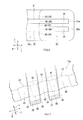
- FIG. 1 is an external perspective view of a piezoelectric vibrator according to an embodiment of the present invention
- FIG. 2 is an inside structure view of the piezoelectric vibrator shown in FIG. 1 ;
- FIG. 3 is a cross-sectional view of the piezoelectric vibrator taken along A-A line of FIG. 2 ;
- FIG. 4 is an exploded perspective view of the piezoelectric vibrator shown in FIG. 1 ;
- FIG. 5 is an enlarged perspective view of tip portions of vibrating arm portions in a piezoelectric vibrating piece shown in FIG. 4 ;
- FIG. 6 is an upper surface view shown by enlarging the periphery of a concave portion shown in FIG. 2 ;
- FIG. 7 is an enlarged perspective view showing the relation between the vibrating arm portions and the concave portion shown in FIG. 6 ;
- FIG. 8 is a view showing a modification example of clearance portions formed in an opening edge portion of the concave portion
- FIG. 9 is a view showing a modification example of clearance portions formed in the opening edge portion of the concave portion
- FIG. 10 is a view showing a modification example of clearance portions formed in the opening edge portion of the concave portion
- FIG. 11 is a view showing a modification example of clearance portions formed in the opening edge portion of the concave portion
- FIG. 12 is a view showing a modification example of clearance portions formed in the opening edge portion of the concave portion
- FIG. 13 is a view showing a modification example of the piezoelectric vibrating piece
- FIG. 14 is a structure view of an oscillator according to an embodiment of the present invention.
- FIG. 15 is a structure view of an electronic apparatus according to an embodiment of the present invention.
- FIG. 16 is a structure view of a radio timepiece according to an embodiment of the present invention.
- FIG. 17 is a view for explaining a related art.
- FIG. 18 is a view for explaining the related art.
- a piezoelectric vibrator 1 is a surface-mount type vibrator as a ceramic package type including a package 2 having an airtightly-sealed cavity C inside and a tuning-fork type piezoelectric vibrating piece 3 housed inside the cavity C.
- the piezoelectric vibrator 1 is formed to have an approximately rectangular parallelepiped shape, in which a longitudinal direction of the piezoelectric vibrator 1 is referred to as a length direction L, a short side direction is referred to as a width direction W and a direction orthogonal to the length direction L and the width direction W is referred to as a thickness direction T in plan view in the embodiment.
- the package 2 includes a package body (base member) 5 and a lid member 6 bonded to the package body 5 and forming the cavity C with respect to the package body 5 .
- the package body 5 includes a first base substrate 10 and a second base substrate 11 which are bonded to each other in an overlapped state, and a seal ring 12 bonded onto the second base substrate 11 .
- the first base substrate 10 is a substrate made of ceramics formed in an approximately rectangular shape in plan view.
- the second base substrate 11 is a substrate made of ceramics formed in an approximately rectangular shape in plan view which is the same shape as the first base substrate 10 , being integrally bonded by sintering and the like in an overlapped state on the first base substrate 10 .
- notch portions 15 having a 1 ⁇ 4 arc shape in plan view are formed over the whole thickness direction T of both substrates 10 and 11 .
- the first base substrate 10 and the second base substrate 11 are formed by, after overlapping two ceramic substrates in a wafer shape and bonding them to each other, forming plural through holes penetrating both ceramic substrates in a matrix state, then, cutting both ceramic substrates in a lattice based on respective through holes. At this time, as the through hole is divided into four, the above notch portions 15 are formed.
- An upper surface of the second base substrate 11 is a mount surface 11 a on which a piezoelectric vibrating piece 3 is mounted.
- the first base substrate 10 and the second base substrate 11 are made of ceramics, and as specific ceramic materials, for example, HTTC (High Temperature Co-Fired Ceramic) made of alumina, LTC (Low Temperature Co-Fired Ceramic) made of glass ceramic and so on can be cited.
- HTTC High Temperature Co-Fired Ceramic
- LTC Low Temperature Co-Fired Ceramic
- the seal ring 12 is a conductive frame-shaped member slightly smaller than an outer shape of the first base substrate 10 and the second base substrate 11 , which is bonded to the mount surface 11 a of the second base substrate 11 .
- the seal ring 12 is bonded on the mount surface 11 a by baking using brazing materials such as silver brazing, solder and so on, or bonded by welding to a metal bonding layer formed (by using, for example, electrolytic plating and electroless plating as well as deposition, sputtering and so on) on the mount surface 11 a.
- the material for the seal ring 12 for example, nickel base alloy and so on can be cited.
- the material can be selected from Kovar, Elinvar, Invar, 42-alloy and so on.
- a material having a thermal expansion coefficient close to the first base substrate 10 and the second base substrate 11 made of ceramics is preferably selected as the material for the seal ring 12 .
- the first base substrate 10 and the second base substrate 11 is used as the first base substrate 10 and the second base substrate 11 , it is preferable that Kovar with a thermal expansion coefficient of 5.2 ⁇ 10 ⁇ 6 PC or 42-alloy with a thermal expansion coefficient of 4.5 to 6.5 ⁇ 10 ⁇ 6 PC is used for the seal ring 12 .
- the rid member 6 is a substrate overlapped on the seal ring 12 , which is airtightly bonded to the package body 5 by the bonding to the seal ring 12 . Then, space defined by the lid member 6 , the seal ring 12 and the mount surface 11 a of the second base substrate 11 functions as the cavity C which is airtightly sealed.
- a welding method of the lid member 6 seam welding performed by allowing a roller electrode to touch, laser welding, ultrasonic welding and so on can be cited.
- a bonding layer made of nickel, gold and the like which are conformable to each other is preferably formed at least on a lower surface of the lid member 6 and an upper surface of the seal ring 12 respectively.
- a pair of electrode pads 20 A and 20 B which are connecting electrodes with respect to the piezoelectric vibrating piece 3 are formed on the mount surface 11 a of the second base substrate 11 with a gap in the width direction W as well as a pair of external electrodes 21 A and 21 B are formed on a lower surface of the first base portion 10 with a gap in the length direction L.
- the electrode pads 20 A, 20 B and the external electrodes 21 A, 21 B are each a single-layer film made of a single metal or a stacked-layer film in which different metals are stacked which are formed by, for example, deposition, sputtering and so on, which are electrically connected to each other.
- first base substrate 10 In the first base substrate 10 , one first through electrode 22 A electrically connected to one external electrode 21 A and penetrating the first base substrate 10 in the thickness direction T is formed.
- second base substrate 11 In the second base substrate 11 , one second through electrode 23 A electrically connected to one electrode pad 20 A and penetrating the second base substrate 11 in the thickness direction T is formed.
- one connecting electrode 24 A connecting one first through electrode 22 A to one second through electrode 23 A is formed between the first base substrate 10 and the second base substrate 11 . Accordingly, one electrode pad 20 A and one external electrode 21 A are electrically connected to each other.
- the other first through electrode 22 B electrically connected to the other external electrode 21 B and penetrating the first base substrate 10 in the thickness direction T is formed.
- the other second through electrode 23 B electrically connected to the other electrode pad 20 B and penetrating the second base substrate 11 in the thickness direction T is formed.
- the other connecting electrode 24 B connecting the other first through electrode 22 B to the other second through electrode 23 B is formed between the first base substrate 10 and the second base substrate 11 . Accordingly, the other electrode pad 20 B and the external electrode 21 B are electrically connected to each other.
- the other connecting electrode 24 B is patterned, for example, so as to extend below the seal ring 12 along the seal ring 12 for avoiding a later-described concave portion 40 .
- the piezoelectric vibrating piece 3 is a tuning-fork type vibrating piece made of piezoelectric materials such as quartz crystal, lithium tantalate and lithium niobate, including a pair of vibrating arm portions 30 and 31 arranged in parallel in the width direction W with tip portions 30 a and 31 a as free ends, and a base portion 32 cantilever-supporting a base-end portions 30 b and 31 b side (root side) of the pair of vibrating arm portions 30 and 31 integrally.
- a tuning-fork type vibrating piece made of piezoelectric materials such as quartz crystal, lithium tantalate and lithium niobate, including a pair of vibrating arm portions 30 and 31 arranged in parallel in the width direction W with tip portions 30 a and 31 a as free ends, and a base portion 32 cantilever-supporting a base-end portions 30 b and 31 b side (root side) of the pair of vibrating arm portions 30 and 31 integrally.
- the pair of vibrating arm portions 30 and 31 extends along length direction L in a state of having a given arm width in the width direction W respectively, and a not-shown pair of excitation electrodes for vibrating the pair of vibrating arm portions 30 and 31 is formed on outer surfaces thereof.
- the excitation electrodes are also formed on edge-line portions and side surfaces of the vibrating arm portions 30 and 31 . It is also preferable that groove portions extending from the base-end portions 30 b and 31 b side to the tip portions 30 a and 30 b side are formed on the outer surfaces of the vibrating arm portions 30 and 31 in order to improve electric-field efficiency and reduce an R-value in the piezoelectric vibrating piece 3 .
- the base portion 32 cantilever-supports the base-end portions 30 b and 31 b side of the pair of vibrating arm portions 30 and 31 as described above, and functions as a mount portion used at the time of mounting the piezoelectric vibrating piece 3 . Then, a not-shown pair of mount electrodes is formed on an outer surface of the base portion 32 in a state of electrically connecting to the pair of excitation electrodes respectively.
- the pair of mount electrodes is electrically connected to the pair of electrode pads 20 A and 20 B. Accordingly, the piezoelectric vibrating piece 3 is cantilever-supported in a state of being floated from the mount surface 11 a of the second base substrate 11 and is electrically connected to the pair of electrode pads 20 A and 20 B respectively.
- the pair of vibrating arm portions 30 and 31 vibrates in the direction (width direction W) moving close to and away from each other at a given resonant frequency due to the interaction between these excitation electrodes.
- each of the pair of vibrating arm portions 30 and 31 is a vibrating member having a rectangular shape in cross section and extending along the length direction L with a fixed arm width and a fixed thickness, having one main surface (lower surface) 35 a facing the mount surface 11 a of the second base substrate 11 , the other main surface (upper surface) 35 b opposite to the one main surface 35 a in the thickness direction T and two side surfaces 35 c facing in the width direction W.
- two edge-line portions (corner portions) 36 extending over the entire length from the base end portions 30 b , 31 b to the tip portions 30 a , 31 a are formed. That is, the pair of vibrating arm portions 30 and 31 has a total of four edge-line portions 36 .
- the edge-line portions 36 are fragile in strength, therefore, a chip, a crack and the like easily occur due to structural characteristics.
- the concave portion 40 is provided at a region facing the tip portions 30 a and 31 a of the pair of vibrating arm portions 30 and 31 , which is for avoiding contact of the tip portions 30 a and 31 a of the vibrating arm portions 30 and 31 occurring when the vibrating arm portions 30 and 31 are displaced (bending deformation) in the thickness direction T (a state indicated by a dotted line shown in FIG. 3 ) due to an external impact such as falling.
- the concave portion 40 is a through hole penetrating the second base substrate 11 as well as formed to have a square shape with rounded four corners in plan view inside the seal ring 12 .
- the concave portion 40 opens to the cavity C side.
- contact portions 41 contacted by one main surfaces 35 a and clearance portions 42 for avoiding contact with the four edge-line portions 36 when the pair of vibrating arm portions 30 and 31 are displaced in the thickness direction T are respectively formed.
- three clearance portions 45 which are concavely formed (eaten) from the tip portions 30 a and 31 a side of the vibrating arm portions 30 and 31 toward the base-end portions 30 b and 31 b side are formed at intervals in the width direction W in the opening edge portion positioned on the base-end portion side of the piezoelectric vibrating piece 3 in a peripheral wall of the concave portion 40 .
- Each of respective clearance portions 45 is formed in the same depth as the concave portion 40 and is integrally formed with the concave portion 40 in a concave state to have an arc or scallop shape in plan view.
- the clearance portion 45 positioned at the center of the width direction W in these three clearance portions 45 is formed at a portion corresponding to the edge-line portions 36 positioned inside in the width direction W (a lower position of the edge-line portions 36 ) in the pair of vibrating arm portions 30 and 31 , and the remaining two clearance portions 45 are formed at portions corresponding to the edge-line portions 36 positioned outside in the width direction W in the pair of vibrating arm portions 30 and 31 .
- the “portions corresponding to the edge-line portions” indicate portions intersecting with the vibrating arm portions 30 and 31 and neighboring portions thereof when seeing the edge-line portions 36 from a normal-line direction of the mount surface.
- the portions indicate intersecting portions between the opening edge portion and regions through which the edge-line portions pass at the time of displacement.
- the portions indicate lower portions of the edge-line portions (and neighboring portions thereof).
- the clearance portions 42 are formed so as to correspond to respective edge-line portions 36 in a manner of avoiding contact with the total of four edge-line portions 36 included in the pair of vibrating arm portions 30 and 31 .
- the clearance portion 42 positioned at the center of the width direction W is a common clearance portion for avoiding contact with two edge-line portions 36 .
- the clearance portions 45 are provided at positions corresponding to all edge-line portions 36 in this case, the number and arrangement of clearance portions 45 are not limited to this.
- the piezoelectric vibrator 1 When the piezoelectric vibrator 1 having the above structure is activated, a given drive voltage is applied to external electrodes 21 A and 21 B formed in the first base substrate 10 . Accordingly, it is possible to allow electric current to flow in the excitation electrodes of the piezoelectric vibrating piece 3 , which can vibrate the pair of vibrating arm portions 30 and 31 in a direction moving close to or away from each other at a predetermined frequency. Additionally, the piezoelectric vibrator 1 can be used as a time source, a timing source of a control signal, a reference-signal source and so on by utilizing the vibration of the pair of vibrating arm portions 30 and 31 .
- the piezoelectric vibrator 1 even when an external impact due to falling and so on is transmitted to the piezoelectric vibrating piece 3 and the vibrating arm portions 30 and 31 are displaced in the thickness direction T, the displacement of the piezoelectric vibrating piece 3 is absorbed by the opening edge portion of the concave portion 40 as the concave portion 40 is formed on the mount surface 11 a of the package body 5 , and it is possible to avoid the tip portions 30 a and 31 a of the vibrating arm portions 30 and 31 which are liable to be largely displaced from contacting the package body 5 .
- the contact portions 41 and the clearance portions 42 are respectively formed in the opening edge portion of the concave portion 40 , therefore, it is possible to allow one main surfaces 35 a of the vibrating arm portions 30 and 31 to contact the contact portions 41 while avoiding contact with respect to the edge-line portions 36 which are fragile in strength by utilizing the clearance portions 42 when the vibrating arm portions 30 and 31 are displaced in the thickness direction T. At this time, it is possible to allow only portions apart from the edge-line portions 36 in one main surfaces 35 a (vicinities of the center in the width W) to contact the contact portions, not allowing one main surfaces 35 a to contact the contact portions across the entire width.
- the displacement of the vibrating arm portions 30 and 31 can be absorbed by the contact with respect to the contact portions 41 and thus converges smoothly while suppressing occurrence of a crack, a chip and the like not only at the tip portions but also the edge-line portions 36 in the piezoelectric vibrating piece 3 , therefore, excessive displacement of the tip portions 30 a and 31 a can be prevented as well as the vibrating arm portions 30 and 31 can be smoothly restored to an original state.
- the piezoelectric vibrating piece 3 is mounted on the mount surface 11 a in an inclined state to some degree, the occurrence of a crack, a chip and so on can be suppressed as the contact with respect to the edge-line portions 36 can be avoided by utilizing the clearance portions 42 .
- the piezoelectric vibrator 1 capable of preventing unintended frequency variation and so on of the piezoelectric vibrating piece 3 and having high performance and impact resistance while securing good vibration characteristics.
- the clearance portions 42 are formed so as to correspond to all respective edge-line portions 36 which are four in total, the contact of the edge-line portions 36 can be avoided even when the piezoelectric vibrating piece 3 is mounted on the mount surface 11 a in a state of being inclined to either side in the width direction W, which can easily suppress occurrence of a crack, a chip and so on. Accordingly, it is possible to efficiently prevent frequency variation and the like of the piezoelectric vibrating piece 3 and the work of mounting the piezoelectric vibrating piece 3 can be easily performed.
- the clearance portions 42 which are concave to have an arc shape in plan view
- the shape of the clearance portions 42 is not limited to the arc shape in plan view.
- the clearance portion 42 may be formed to have a V-shape in plan view as shown in FIG. 8 as well as to have a trapezoid-shape in plan view as shown in FIG. 9 .
- Other shapes can be also applied. The same operation and effect can be obtained in these cases.
- clearance portions 42 corresponding to all four edge-line portions 36 are formed by forming three clearance portions 42 in the above embodiment, it is not limited to this, and it is also possible to form the clearance portions 42 corresponding to all four edge-line portions 36 , for example, by forming four clearance portions 42 as shown in FIG. 10 .
- the clearance portions 42 are formed so as to corresponding to the total four edge-line portions 36 in the above embodiment, however, it is also preferable to form the clearance portion 42 so as to correspond to at least one edge-line portion 36 in each of the vibrating arm portions 30 and 31 .
- the clearance portions 42 are formed so as to correspond all four edge-line portions 36 as in the above embodiment.
- the concave portion 40 and the clearance portions 42 are integrally formed in the above embodiment, however, it is not limited to this. It is also preferable that the clearance portions 42 are formed by, for example, performing deep groove milling of the mount surface 11 a so as to overlap with the opening edge portion of the concave portion 40 .
- the concave portion 40 and the clearance portions 42 can be formed simultaneously and easily by performing punching processing of the second base substrate 11 by using a pressing machine and so on in the above embodiment, therefore, the formation of the clearance portions 42 is not troublesome, and further, the clearance portions 42 with a refined shape can be easily formed with accuracy.
- the outer shape of the piezoelectric vibrating piece 3 is not limited to the shape of the above embodiment and can be appropriately changed.
- a so-called grooved piezoelectric vibrating piece 3 in which groove portions are formed respectively on one main surfaces 35 a and the other main surfaces 35 b a so-called notched piezoelectric vibrating piece 3 in which notches are formed in the vicinity of a connecting portion with respect to the base end portions 30 b and 31 b of the pair of the vibrating arm portions 30 and 31 in the base portion 32 from both side surfaces in the width direction W to the center in the width direction W respectively, and a so-called hammerhead type piezoelectric vibrating piece 3 in which hammer portions with an enlarged width wider than the base end portions 30 b and 31 b are formed on the tip portions 30 a and 31 a of the vibrating arm portions 30 and 31 .
- the excitation electrodes are necessary on the outer surfaces of the vibrating arm portions in any shape of the piezoelectric vibrating piece 3 selected from the above. According to the embodiment of the present invention, even when the excitation electrodes are formed in the edge-line portion of the vibrating arm portions, there is no danger that a fracture and so on occur by the contact between the excitation electrodes and the opening edge portion because the contact between the edge-line portions and the opening edge portion of the concave portion can be avoided. Furthermore, when the piezoelectric vibrating piece is displaced in the thickness direction and the vibrating arm portions contact the opening edge portion, a fracture and so on of the excitation electrode can be positively avoided by allowing the contact portions of the opening edge portion to contact regions where the excitation electrodes are not formed in the vibrating arm portions.
- a side-arm type piezoelectric vibrating piece 3 can be formed, in which a pair of side arms 50 extending along the length direction L are integrally formed with the base portion 32 on both sides of the base portion 32 in the width direction W.
- tip portions 50 a of the side arms 50 are allowed to function as mount portions, and the piezoelectric vibrating piece 3 can be mounted through the mount portions by forming the electrode pads 20 A and 20 B so as to correspond to positions of the tip portions 50 a of the side arms 50 .
- An oscillator 100 uses the piezoelectric vibrator 1 as a resonator electrically connected to an integrated circuit 101 as shown in FIG. 14 .
- the oscillator 100 includes a substrate 103 on which an electronic component 102 such as a capacitor is mounted.
- the integrated circuit 101 for the oscillator is mounted on the substrate 103 and the piezoelectric vibrator 1 is mounted in the vicinity of the integrated circuit 101 .
- the electronic component 102 , the integrated circuit 101 and the piezoelectric vibrator 1 are electrically connected to one another by a not-shown wiring pattern. Note that respective components are molded by a not-shown resin.
- the piezoelectric vibrating piece 3 inside the piezoelectric vibrator 1 vibrates.
- the vibration is converted into an electric signal by piezoelectric characteristics possessed by the piezoelectric vibrating piece 3 and inputted into the integrated circuit 101 as the electric signal.
- Various processing is performed to the inputted electric signal by the integrated circuit 101 and outputted as a frequency signal. Accordingly, the piezoelectric vibrator 1 functions as the resonator.
- an RTC (real time clock) module is selectively set according to a request, thereby adding functions of controlling a single-function oscillator for a timepiece, operation dates, time of the device or external devices, as well as providing time, a calendar and so on.
- the oscillator 100 includes the above-described piezoelectric vibrator 1 , therefore, the oscillator 100 having improved performance and impact resistance can be obtained in the same manner.
- FIG. 15 An electronic apparatus according to an embodiment of the present invention will be explained with reference to FIG. 15 .
- the explanation will be made by citing a portable information device 110 including the above piezoelectric vibrator 1 as an example of the electronic apparatus.
- the portable information device 110 is typified by a cellular phone, which is obtained by developing and improving a wrist watch in related art.
- An appearance of the device is analogous to a wrist watch, and a liquid crystal display is arranged at a portion corresponding to an hour plate to thereby display present time and the like on a screen thereof.
- communication can be performed similarly as a cellular phone in related art, by removing the device from a wrist and using a speaker and a microphone included in an inside portion of a band.
- size and weight of the device has been drastically reduced as compared with the related-art cellular phone.
- the portable information device 110 includes the piezoelectric vibrator 1 and a power supply unit 111 for supplying electric power as shown in FIG. 15 .
- the power supply unit 111 is formed by, for example, a lithium secondary battery.
- a control unit 112 performing various control, a timer unit 113 performing counting of time and the like, a communication unit 114 performing communication with the outside, a display unit 115 displaying various information and a voltage detection unit 116 detecting voltages of respective function units are connected in parallel to the power supply unit 111 . Then, electric power is supplied to respective function units by the power supply unit 111 .
- the control unit 112 controls respective function units to control operations in the entire system such as transmission/reception of audio data and measurement/display of present time.
- the control unit 112 also includes a ROM in which programs are previously written, a CPU reading and executing programs written in the ROM, a RAM used as a work area of the CPU and so on.
- the timer unit 113 includes an integrated circuit having an oscillating circuit, a register circuit, a counter circuit, an interface circuit and so on, and the piezoelectric vibrator 1 .
- the piezoelectric vibrating piece 3 vibrates, and the vibration is converted into an electric signal by piezoelectric characteristics possessed by quartz crystal to be inputted into the oscillating circuit as the electric signal.
- An output of the oscillating circuit is binarized and counted by the register circuit and the counter circuit. Then, signal transmission/reception is performed with respect to the control unit 112 through the interface circuit, and present time/present date or calendar information and so on are displayed on the display unit 115 .
- the communication unit 114 has similar functions as the related-art cellular phone, including a radio unit 117 , an audio processing unit 118 , a switching unit 119 , an amplification unit 120 , an audio input/output unit 121 , a telephone-number input unit 122 , a ring-tone generation unit 123 and a call-control memory unit 124 .
- the radio unit 117 performs transmission/reception of various data such as audio data with respect to base stations through an antenna 125 .
- the audio processing unit 118 encodes and decodes an audio signal inputted from the ratio unit 117 or the amplification unit 120 .
- the amplification unit 120 amplifies a signal inputted from the audio processing unit 118 or the audio input/output unit 121 to a given level.
- the audio input/output unit 121 is formed by a speaker, a microphone and the like, amplifying a ring tone or receiver audio as well as collecting audio.
- the ring-tone generation unit 123 generates the ring tone in accordance with calling from the base station. Only when receiving a call, the switching unit 119 switches the amplification unit 120 connected to the audio processing unit 118 to the ring-tone generation unit 123 , the ring tone generated in the ring-tone generation unit 123 is outputted to the audio input/output unit 121 through the amplification unit 120 .
- the call-control memory unit 124 stores programs concerning incoming/outgoing call control of communication.
- the telephone-number input unit 122 has, for example, number keys from “0” to “9” and other keys, and a telephone number of a called party and so on is inputted by pressing these number keys.
- the voltage detection unit 116 detects the voltage decrease and notifies the control unit 112 of the decrease.
- the given voltage value set at this time is a value previously set as the minimum voltage necessary for stably operating the communication unit 114 , which is for example, approximately 3V.
- the control unit 112 which has received notification of voltage decrease from the voltage detection unit 116 prohibits operations of the radio unit 117 , the audio processing unit 118 , the switching unit 119 and the ring-tone generation unit 123 . Particularly, stop of the operation of the radio unit 117 having large power consumption is fundamental. Moreover, information indicating that the communication unit 114 is unavailable due to the insufficient remaining amount of a battery is displayed on the display unit 115 .
- the display may be made as a message of characters, or it is also preferable that a cross mark is put as a more intuitive display on a telephone icon displayed on an upper part of a display surface of the display unit 115 .
- the portable information device 110 includes the above-described piezoelectric vibrator 1 , therefore, the portable information device 110 having improved performance and impact resistance can be obtained in the same manner.
- a radio timepiece 130 includes the piezoelectric vibrator 1 electrically connected to a filter unit 131 as shown in FIG. 16 , which is a timepiece having a function of receiving standard radio waves including timepiece information and displaying accurate time after performing automatic correction.
- transmitting stations which transmit standard radio waves, in Fukushima prefecture (40 kHz) and Saga prefecture (60 kHz), and respectively transmit standard radio waves. Since long waves such as 40 kHz or 60 kHz have both a property to propagate the ground surface and a property to propagate while being reflected between an ionized layer and the ground surface, therefore, a wide range of propagation is achieved, so that the above-described two transmitting stations cover the entire part of Japan.
- An antenna 132 receives a long-wave standard radio wave of 40 kHz or 60 kHz.
- the long standard radio wave is time information referred to as a time code and subjected to an AM modulation to a carrier wave of 40 kHz or 60 kHz.
- the received long standard wave is amplified by an amplifier 133 and is filtered and synchronized by the filter unit 131 having plural piezoelectric vibrators 1 .
- the piezoelectric vibrators 1 respectively include quartz vibrator units 138 and 139 having resonant frequencies of 40 kHz and 60 kHz which are the same as the above-described carrier frequencies, respectively.
- the filtered signal having a given frequency is detected and demodulated by a detection/rectification circuit 134 .
- the time code is acquired through a waveform shaping circuit 135 , and counted by a CPU 136 .
- the CPU 136 reads information such as the current year, day of year, day of the week, time of day and the like. The read information is reflected on an RTC 137 , and correct time of day information is displayed.
- vibrators having the above-described turning-fork type structure are suitable for the quarts vibrator units 138 and 139 .
- the radio timepiece 130 according to the embodiment has the above-described piezoelectric vibrator 1 , therefore, the radio timepiece 130 having improved performance and impact resistance can be obtained in the same manner
- the ceramic-package type piezoelectric vibrator 1 has been cited as an example in the above embodiment, however, it is not limited to this, and for example, a glass-package type piezoelectric vibrator may be applied.
- the base substrate is formed by two substrates of the first base substrate 10 and the second base substrate 11
- the base substrate is formed by one substrate and the concave portion 40 is formed on the mount surface 11 a .
- the structure of two substrates including the first base substrate 10 and the second base substrate 11 is preferable as described above.
- the concave portion 40 can be easily formed by forming a through hole in the second base substrate 11 , then, by bonding both base substrates to each other, therefore, processes and time to be spent for forming the concave portion can be reduced.
Landscapes
- Physics & Mathematics (AREA)
- Acoustics & Sound (AREA)
- Piezo-Electric Or Mechanical Vibrators, Or Delay Or Filter Circuits (AREA)
Abstract
Description
- This application claims benefit of priority under 35 U.S.C. §119 to Japanese Patent Application No. 2012-207260, filed Sep. 20, 2012, the entire content of which is hereby incorporated by reference.
- 1. Field of the Invention
- The present invention relates to a piezoelectric vibrator, an oscillator, an electronic apparatus and a radio timepiece.
- 2. Description of the Related Art
- For example, in a cellular phone or portable information terminal devices, a piezoelectric vibrator using crystal and so on is often used as a time source, a timing source of a control signal and the like, a reference-signal source and so on. As this type of piezoelectric vibrator, a tuning-fork type piezoelectric vibrator which is airtightly sealed in a package in which a cavity is formed is known.
- In the above package, one substrate in which a concave portion is formed is overlapped on the other substrate and both substrates are bonded to each other, thereby forming a cavity by using the concave portion.
- The piezoelectric vibrating piece includes a pair of vibrating arm portions arranged side by side in parallel in a width direction and a base portion cantilever-supporting a base-end portion side of the pair of vibrating arm portions, in which the pair of vibrating arm portions vibrates (swings) close to and away from each other in a width direction from the base-end portion side as an original point at a given frequency.
- Incidentally, as cellular phone and portable information terminal devices are becoming small in size in recent years, the piezoelectric vibrating piece is also planned to be further small and thin in size. Accordingly, a clearance between the piezoelectric vibrating piece and a mount surface (inner surface of the package) in a thickness direction is becoming extremely narrow (for example, approximately 20 μm to 100 μm). As a result, when an impact due to falling is added to the piezoelectric vibrator, there is a danger that the vibrating arm portions are displaced (bending deformation) and tip portions of the vibrating arm portions as free ends contact the inner surface of the package. In this case, a crack, a chip and so on may occur at the tip portions of the vibrating arm portions due to an impact at the time of contact, which may cause frequency variation or may cause a breakage of the vibrating arm portions themselves in the worst case.
- Accordingly, as countermeasures against the above, it is known that, for example, a concave portion for avoiding the touching between the tip portion of vibrating arm portion and a base member is formed in a portion corresponding to the tip portions of the vibrating arm portions on the mount surface as shown in JP-A 2010-119127 (Patent Document 1).
- In
Patent Document 1, there is disclosed that, even when the vibration arm portion is displaced in the thickness direction due to the impact such as falling, it is easy to avoid the contact between the tip portion of the vibrating arm portion and the base member as a corner portion (opening edge portion) of the concave portion contacts an intermediate portion of the vibrating arm. - However, there are the following problems in the above related art.
- That is, when the piezoelectric vibrating piece is mounted on the mount surface of the base member, the piezoelectric vibrating piece is placed with respect to metal bumps, conductive adhesive and so on applied on the mount surface to be fixed thereon. At this time, mounting is performed so that the piezoelectric vibrating piece is arranged in parallel to the mount surface, however, it has been found that the piezoelectric vibrating piece is actually mounted in a state of being inclined to the mount surface in many cases by being affected by a point that the metal bumps and the conductive adhesive are materials with liquidity, variation in mount conditions, a design error of the piezoelectric vibrating piece, a design error of the base member, specifications of a manufacturing device and so on.
- The above points will be explained in more detail with reference to
FIG. 17 andFIG. 18 . - First, in an ideal case in which the piezoelectric vibrating piece is mounted in parallel to the mount surface of the base member,
main surfaces 200 a of vibratingarm portions 200 are parallel to the mount surface as shown inFIG. 17 , therefore, when the vibratingarm portions 200 are displaced due to an external impact and so on, a line contact between acorner portion 201 a of aconcave portion 201 and themain surfaces 200 a of the vibratingarm portions 200 is possible. - However, as the piezoelectric vibrating piece is mounted in a state of being inclined to some degree as described above, particularly, in a state of being inclined in a width direction of the piezoelectric vibrating piece in many cases, the
main surfaces 200 a of the vibratingarm portions 200 are actually inclined to the mount surface as shown inFIG. 18 . In such case, it is difficult to make a line contact between thecorner portion 201 a of theconcave portion 201 and themain surfaces 200 a of the vibratingarm portions 200 when the vibratingarm portions 200 are displaced due to the external impact and so on. - Accordingly, it has been found that only edge-
line portions 200 b of the vibratingarm portions 200 contact thecorner portion 201 a of theconcave potion 201 and that stress is locally acted on the edge-line portions 200 b which are fragile in strength. As a result, a crack, a chip and the like occur in the edge-line portions 200 b as the stress is concentrated on the edge-line portions 200 b, which leads to reduction of strength and vibration characteristics of the piezoelectric vibrating piece. That is, it is difficult to positively prevent occurrence of a crack, a chip and the like in the piezoelectric vibrating piece at the time of receiving the external impact when there is variation in mounting accuracy of the piezoelectric vibrating piece in related art. - In order to solve the above problems, an object of the present invention is to provide a piezoelectric vibrator, which is capable of preventing the touching between the piezoelectric vibrating piece and the base member due to the external impact and the like and preventing occurrence of a crack, a chip and the like even when there is variation in mounting accuracy of the piezoelectric vibrating piece to be mounted on the mount surface on the base, and also to provide an oscillator, an electronic apparatus and a radio timepiece having the piezoelectric vibrator.
- The present invention provides the following means for solving the above problems.
- (1) A piezoelectric vibrator according to an embodiment of the present invention includes a base member, a lid member bonded to the base member in an overlapped state and forming an airtightly-sealed cavity with respect to the base member, and a piezoelectric vibrating piece having a pair of vibrating arm portions and a base portion integrally supporting base end portions of the pair of vibrating arm portions in a length direction, being mounted on a mount surface of the base member inside the cavity, in which a concave portion is formed on the mount surface of the base member at a region facing tip portions of the piezoelectric vibrating piece, and clearance portions eaten in a direction of the base-end portion side are formed at portions corresponding to edge-line portions of the vibrating arm portions in an opening edge portion arranged on the base-end portion side of the piezoelectric vibrating piece in opening edge portions of the concave portion when seen from a normal-line direction of the mount surface of the base member.
- In the piezoelectric vibrator according to an embodiment of the present invention, in the case where an impact due to falling and so on is transmitted to the piezoelectric vibrating piece and the vibrating arm portions are displaced in the thickness direction, the concave portion is formed in the mount surface and the opening edge portion of the concave portion contacts the vibrating arm portions displaced in the thickness direction (portions other than the tip portions), therefore, it is possible to avoid the tip portions of the vibrating arm portions which are liable to be largely displaced from touching the base member and being broken.
- Moreover, the clearance portions eaten in the direction of the base-end portion side are formed at portions corresponding to the edge-line portions of the vibrating arm portions when seen from the normal-line direction of the mount surface of the base member. Accordingly, there is no danger that the edge-line portions of the vibrating arm portions contact the opening edge portion of the concave portion when the piezoelectric vibrating piece is displaced in the thickness direction in a state where the piezoelectric vibrating piece is mounted in an inclined state in the width direction. That is, occurrence of a crack, a chip and so on in the edge-line portions can be prevented as stress is not concentrated on the edge lines as in related art. Therefore, the strength and vibration characteristics of the piezoelectric vibrating piece can be improved.
- Note that, the “portions corresponding to the edge-line portions of the vibrating arm portions” referred to in this case indicate portions intersecting with the edge-line portions of the vibrating arm portions when seen from the normal-line direction of the mount surface and neighboring portions thereof. That is, the portions indicate regions through which the edge-line portions pass when displaced in the thickness direction of the vibrating arm portions. Moreover, the edge-line portions referred to in this case include at least the edge-line portions facing the mount surface in plural edge-line portions included in the vibrating arm portions.
- Accordingly, it is possible to suppress occurrence of a crack, a chip and so on not only in the tip portions but also in the edge-line portions of the vibrating arm portions, therefore, unintended frequency variation of the piezoelectric vibrating piece can be prevented and the piezoelectric vibrator having high performance and impact resistance while securing good vibration characteristics can be provided.
- (2) In the piezoelectric vibrator according to the embodiment, it is preferable that the clearance portions are formed so as to correspond to respective edge-line portions of the pair of vibrating arm portions.
- In this case, as the clearance portions are formed so as to correspond to respective edge-line portions, the contact between the edge-line portions and the opening edge portion can be avoided and the occurrence of a crack, a chip and the like can be easily suppressed even when the piezoelectric vibrating piece is mounted on the mount surface in a state of being inclined to either side in the width direction. Therefore, it is possible to increase the efficiency in the work of mounting the piezoelectric vibrating piece.
- (3) In the piezoelectric vibrator according to the embodiment, it is preferable that the clearance portions and the concave portion are the formed to be approximately the same depth.
- In this case, as the clearance portions and the concave portion can be formed simultaneously and easily by using a pressing machine or the like, the clearance portions and the concave portion can be formed in a simple process and the clearance portions with a refined shape can be easily formed with accuracy.
- (4) An oscillator according to an embodiment of the present invention includes the piezoelectric vibrator according to the embodiment of the present invention which is electrically connected to an integrated circuit as a resonator.
- (5) An electronic apparatus according to an embodiment of the present invention includes the piezoelectric vibrator according to the embodiment of the present invention which is electrically connected to a timer unit.
- (6) A radio timepiece according to an embodiment of the present invention includes the piezoelectric vibrator according to the embodiment of the present invention which is electrically connected to a filter unit.
- As the oscillator, the electronic apparatus and the radio timepiece according to the embodiment of the present invention include the above-described piezoelectric vibrator, therefore, the performance and the impact resistance can be increased in the same manner.
- According to the embodiment of the present invention, it is possible to provide the piezoelectric vibrator, which is capable of preventing the touching between the piezoelectric vibrating piece and the base member due to the external impact and so on and preventing occurrence of a crack, a chip and the like even when there is variation in mounting accuracy of the piezoelectric vibrating piece to be mounted on the mount surface on the base, and also to provide the oscillator, the electronic apparatus and the radio timepiece including the piezoelectric vibrator.
-
FIG. 1 is an external perspective view of a piezoelectric vibrator according to an embodiment of the present invention; -
FIG. 2 is an inside structure view of the piezoelectric vibrator shown inFIG. 1 ; -
FIG. 3 is a cross-sectional view of the piezoelectric vibrator taken along A-A line ofFIG. 2 ; -
FIG. 4 is an exploded perspective view of the piezoelectric vibrator shown inFIG. 1 ; -
FIG. 5 is an enlarged perspective view of tip portions of vibrating arm portions in a piezoelectric vibrating piece shown inFIG. 4 ; -
FIG. 6 is an upper surface view shown by enlarging the periphery of a concave portion shown inFIG. 2 ; -
FIG. 7 is an enlarged perspective view showing the relation between the vibrating arm portions and the concave portion shown inFIG. 6 ; -
FIG. 8 is a view showing a modification example of clearance portions formed in an opening edge portion of the concave portion; -
FIG. 9 is a view showing a modification example of clearance portions formed in the opening edge portion of the concave portion; -
FIG. 10 is a view showing a modification example of clearance portions formed in the opening edge portion of the concave portion; -
FIG. 11 is a view showing a modification example of clearance portions formed in the opening edge portion of the concave portion; -
FIG. 12 is a view showing a modification example of clearance portions formed in the opening edge portion of the concave portion; -
FIG. 13 is a view showing a modification example of the piezoelectric vibrating piece; -
FIG. 14 is a structure view of an oscillator according to an embodiment of the present invention; -
FIG. 15 is a structure view of an electronic apparatus according to an embodiment of the present invention; -
FIG. 16 is a structure view of a radio timepiece according to an embodiment of the present invention; -
FIG. 17 is a view for explaining a related art; and -
FIG. 18 is a view for explaining the related art. - Hereinafter, a piezoelectric vibrator according to an embodiment of the present invention will be explained with reference to the drawings.
- As shown in
FIG. 1 toFIG. 4 , apiezoelectric vibrator 1 according to the embodiment is a surface-mount type vibrator as a ceramic package type including apackage 2 having an airtightly-sealed cavity C inside and a tuning-fork typepiezoelectric vibrating piece 3 housed inside the cavity C. - The
piezoelectric vibrator 1 is formed to have an approximately rectangular parallelepiped shape, in which a longitudinal direction of thepiezoelectric vibrator 1 is referred to as a length direction L, a short side direction is referred to as a width direction W and a direction orthogonal to the length direction L and the width direction W is referred to as a thickness direction T in plan view in the embodiment. - The
package 2 includes a package body (base member) 5 and alid member 6 bonded to thepackage body 5 and forming the cavity C with respect to thepackage body 5. - The
package body 5 includes afirst base substrate 10 and asecond base substrate 11 which are bonded to each other in an overlapped state, and aseal ring 12 bonded onto thesecond base substrate 11. - The
first base substrate 10 is a substrate made of ceramics formed in an approximately rectangular shape in plan view. Thesecond base substrate 11 is a substrate made of ceramics formed in an approximately rectangular shape in plan view which is the same shape as thefirst base substrate 10, being integrally bonded by sintering and the like in an overlapped state on thefirst base substrate 10. - In four corners of the
first base substrate 10 and thesecond base substrate 11,notch portions 15 having a ¼ arc shape in plan view are formed over the whole thickness direction T of bothsubstrates first base substrate 10 and thesecond base substrate 11 are formed by, after overlapping two ceramic substrates in a wafer shape and bonding them to each other, forming plural through holes penetrating both ceramic substrates in a matrix state, then, cutting both ceramic substrates in a lattice based on respective through holes. At this time, as the through hole is divided into four, theabove notch portions 15 are formed. - An upper surface of the
second base substrate 11 is amount surface 11 a on which a piezoelectric vibratingpiece 3 is mounted. - The
first base substrate 10 and thesecond base substrate 11 are made of ceramics, and as specific ceramic materials, for example, HTTC (High Temperature Co-Fired Ceramic) made of alumina, LTC (Low Temperature Co-Fired Ceramic) made of glass ceramic and so on can be cited. - The
seal ring 12 is a conductive frame-shaped member slightly smaller than an outer shape of thefirst base substrate 10 and thesecond base substrate 11, which is bonded to themount surface 11 a of thesecond base substrate 11. Specifically, theseal ring 12 is bonded on themount surface 11 a by baking using brazing materials such as silver brazing, solder and so on, or bonded by welding to a metal bonding layer formed (by using, for example, electrolytic plating and electroless plating as well as deposition, sputtering and so on) on themount surface 11 a. - As materials for the
seal ring 12, for example, nickel base alloy and so on can be cited. Specifically, the material can be selected from Kovar, Elinvar, Invar, 42-alloy and so on. Particularly, a material having a thermal expansion coefficient close to thefirst base substrate 10 and thesecond base substrate 11 made of ceramics is preferably selected as the material for theseal ring 12. For example, when alumina with a thermal expansion coefficient of 6.8×10⁻⁶/° C. is used as thefirst base substrate 10 and thesecond base substrate 11, it is preferable that Kovar with a thermal expansion coefficient of 5.2×10⁻⁶PC or 42-alloy with a thermal expansion coefficient of 4.5 to 6.5×10⁻⁶PC is used for theseal ring 12. - The
rid member 6 is a substrate overlapped on theseal ring 12, which is airtightly bonded to thepackage body 5 by the bonding to theseal ring 12. Then, space defined by thelid member 6, theseal ring 12 and themount surface 11 a of thesecond base substrate 11 functions as the cavity C which is airtightly sealed. - As a welding method of the
lid member 6, seam welding performed by allowing a roller electrode to touch, laser welding, ultrasonic welding and so on can be cited. In order to perform welding between thelid member 6 and theseal ring 12 more reliably, a bonding layer made of nickel, gold and the like which are conformable to each other is preferably formed at least on a lower surface of thelid member 6 and an upper surface of theseal ring 12 respectively. - Incidentally, a pair of
electrode pads piece 3 are formed on themount surface 11 a of thesecond base substrate 11 with a gap in the width direction W as well as a pair ofexternal electrodes first base portion 10 with a gap in the length direction L. - The
electrode pads external electrodes - The above point will be explained in detail.
- In the
first base substrate 10, one first throughelectrode 22A electrically connected to oneexternal electrode 21A and penetrating thefirst base substrate 10 in the thickness direction T is formed. In thesecond base substrate 11, one second throughelectrode 23A electrically connected to oneelectrode pad 20A and penetrating thesecond base substrate 11 in the thickness direction T is formed. Then, one connectingelectrode 24A connecting one first throughelectrode 22A to one second throughelectrode 23A is formed between thefirst base substrate 10 and thesecond base substrate 11. Accordingly, oneelectrode pad 20A and oneexternal electrode 21A are electrically connected to each other. - Additionally, in the
first base substrate 10, the other first throughelectrode 22B electrically connected to the otherexternal electrode 21B and penetrating thefirst base substrate 10 in the thickness direction T is formed. In thesecond base substrate 11, the other second throughelectrode 23B electrically connected to theother electrode pad 20B and penetrating thesecond base substrate 11 in the thickness direction T is formed. Then, the other connectingelectrode 24B connecting the other first throughelectrode 22B to the other second throughelectrode 23B is formed between thefirst base substrate 10 and thesecond base substrate 11. Accordingly, theother electrode pad 20B and theexternal electrode 21B are electrically connected to each other. - The other connecting
electrode 24B is patterned, for example, so as to extend below theseal ring 12 along theseal ring 12 for avoiding a later-describedconcave portion 40. - The piezoelectric vibrating
piece 3 is a tuning-fork type vibrating piece made of piezoelectric materials such as quartz crystal, lithium tantalate and lithium niobate, including a pair of vibratingarm portions tip portions base portion 32 cantilever-supporting a base-end portions arm portions - The pair of vibrating
arm portions arm portions arm portions end portions tip portions arm portions piece 3. - The
base portion 32 cantilever-supports the base-end portions arm portions piece 3. Then, a not-shown pair of mount electrodes is formed on an outer surface of thebase portion 32 in a state of electrically connecting to the pair of excitation electrodes respectively. - As the piezoelectric vibrating
piece 3 having the above structure is mounted through not-shown metal bumps, conductive adhesive and so on, the pair of mount electrodes is electrically connected to the pair ofelectrode pads piece 3 is cantilever-supported in a state of being floated from themount surface 11 a of thesecond base substrate 11 and is electrically connected to the pair ofelectrode pads arm portions - Incidentally, each of the pair of vibrating
arm portions mount surface 11 a of thesecond base substrate 11, the other main surface (upper surface) 35 b opposite to the onemain surface 35 a in the thickness direction T and twoside surfaces 35 c facing in the width direction W. - Accordingly, in portions where one
main surface 35 a intersects with twoside surfaces 35 c in each of the vibratingarm portions base end portions tip portions arm portions line portions 36. In particular, the edge-line portions 36 are fragile in strength, therefore, a chip, a crack and the like easily occur due to structural characteristics. - Note that
reference numerals FIG. 5 for simplifying the drawing. - As shown in
FIG. 2 toFIG. 4 , in themount surface 11 a of thesecond base substrate 11, theconcave portion 40 is provided at a region facing thetip portions arm portions tip portions arm portions arm portions FIG. 3 ) due to an external impact such as falling. Theconcave portion 40 is a through hole penetrating thesecond base substrate 11 as well as formed to have a square shape with rounded four corners in plan view inside theseal ring 12. - The
concave portion 40 opens to the cavity C side. In an opening edge portion positioned on the base-end portion side of the piezoelectric vibratingpiece 3 in opening edge portions,contact portions 41 contacted by onemain surfaces 35 a andclearance portions 42 for avoiding contact with the four edge-line portions 36 when the pair of vibratingarm portions - Specifically, as shown in
FIG. 6 andFIG. 7 , threeclearance portions 45 which are concavely formed (eaten) from thetip portions arm portions end portions piece 3 in a peripheral wall of theconcave portion 40. Each ofrespective clearance portions 45 is formed in the same depth as theconcave portion 40 and is integrally formed with theconcave portion 40 in a concave state to have an arc or scallop shape in plan view. - The
clearance portion 45 positioned at the center of the width direction W in these threeclearance portions 45 is formed at a portion corresponding to the edge-line portions 36 positioned inside in the width direction W (a lower position of the edge-line portions 36) in the pair of vibratingarm portions clearance portions 45 are formed at portions corresponding to the edge-line portions 36 positioned outside in the width direction W in the pair of vibratingarm portions arm portions line portions 36 from a normal-line direction of the mount surface. In other words, the portions indicate intersecting portions between the opening edge portion and regions through which the edge-line portions pass at the time of displacement. In further other words, the portions indicate lower portions of the edge-line portions (and neighboring portions thereof). - That is, the
clearance portions 42 are formed so as to correspond to respective edge-line portions 36 in a manner of avoiding contact with the total of four edge-line portions 36 included in the pair of vibratingarm portions clearance portion 42 positioned at the center of the width direction W is a common clearance portion for avoiding contact with two edge-line portions 36. Though theclearance portions 45 are provided at positions corresponding to all edge-line portions 36 in this case, the number and arrangement ofclearance portions 45 are not limited to this. - When the
piezoelectric vibrator 1 having the above structure is activated, a given drive voltage is applied toexternal electrodes first base substrate 10. Accordingly, it is possible to allow electric current to flow in the excitation electrodes of the piezoelectric vibratingpiece 3, which can vibrate the pair of vibratingarm portions piezoelectric vibrator 1 can be used as a time source, a timing source of a control signal, a reference-signal source and so on by utilizing the vibration of the pair of vibratingarm portions - Additionally, in the
piezoelectric vibrator 1 according to the embodiment, even when an external impact due to falling and so on is transmitted to the piezoelectric vibratingpiece 3 and the vibratingarm portions piece 3 is absorbed by the opening edge portion of theconcave portion 40 as theconcave portion 40 is formed on themount surface 11 a of thepackage body 5, and it is possible to avoid thetip portions arm portions package body 5. Moreover, thecontact portions 41 and theclearance portions 42 are respectively formed in the opening edge portion of theconcave portion 40, therefore, it is possible to allow onemain surfaces 35 a of the vibratingarm portions contact portions 41 while avoiding contact with respect to the edge-line portions 36 which are fragile in strength by utilizing theclearance portions 42 when the vibratingarm portions line portions 36 in onemain surfaces 35 a (vicinities of the center in the width W) to contact the contact portions, not allowing onemain surfaces 35 a to contact the contact portions across the entire width. - Accordingly, the displacement of the vibrating
arm portions contact portions 41 and thus converges smoothly while suppressing occurrence of a crack, a chip and the like not only at the tip portions but also the edge-line portions 36 in the piezoelectric vibratingpiece 3, therefore, excessive displacement of thetip portions arm portions - In particular, even when the piezoelectric vibrating
piece 3 is mounted on themount surface 11 a in an inclined state to some degree, the occurrence of a crack, a chip and so on can be suppressed as the contact with respect to the edge-line portions 36 can be avoided by utilizing theclearance portions 42. - As a result, it is possible to obtain the
piezoelectric vibrator 1 capable of preventing unintended frequency variation and so on of the piezoelectric vibratingpiece 3 and having high performance and impact resistance while securing good vibration characteristics. - In addition, as the
clearance portions 42 are formed so as to correspond to all respective edge-line portions 36 which are four in total, the contact of the edge-line portions 36 can be avoided even when the piezoelectric vibratingpiece 3 is mounted on themount surface 11 a in a state of being inclined to either side in the width direction W, which can easily suppress occurrence of a crack, a chip and so on. Accordingly, it is possible to efficiently prevent frequency variation and the like of the piezoelectric vibratingpiece 3 and the work of mounting the piezoelectric vibratingpiece 3 can be easily performed. - In the above embodiment, the
clearance portions 42 which are concave to have an arc shape in plan view, however, the shape of theclearance portions 42 is not limited to the arc shape in plan view. For example, theclearance portion 42 may be formed to have a V-shape in plan view as shown inFIG. 8 as well as to have a trapezoid-shape in plan view as shown inFIG. 9 . Other shapes can be also applied. The same operation and effect can be obtained in these cases. - Although the
clearance portions 42 corresponding to all four edge-line portions 36 are formed by forming threeclearance portions 42 in the above embodiment, it is not limited to this, and it is also possible to form theclearance portions 42 corresponding to all four edge-line portions 36, for example, by forming fourclearance portions 42 as shown inFIG. 10 . - The
clearance portions 42 are formed so as to corresponding to the total four edge-line portions 36 in the above embodiment, however, it is also preferable to form theclearance portion 42 so as to correspond to at least one edge-line portion 36 in each of the vibratingarm portions - For example, it is possible to form only one
clearance portion 42 as shown inFIG. 11 to thereby avoid contact with the edge-line portions 36 positioned inside in the width direction in respective vibratingarm portions clearance portions 42 as shown inFIG. 12 to thereby avoid contact with the edge-line portions 36 positioned outside in the width direction in respective vibratingarm portions - However, it is preferable to form the
clearance portions 42 so as to correspond all four edge-line portions 36 as in the above embodiment. - Additionally, the
concave portion 40 and theclearance portions 42 are integrally formed in the above embodiment, however, it is not limited to this. It is also preferable that theclearance portions 42 are formed by, for example, performing deep groove milling of themount surface 11 a so as to overlap with the opening edge portion of theconcave portion 40. - However, the
concave portion 40 and theclearance portions 42 can be formed simultaneously and easily by performing punching processing of thesecond base substrate 11 by using a pressing machine and so on in the above embodiment, therefore, the formation of theclearance portions 42 is not troublesome, and further, theclearance portions 42 with a refined shape can be easily formed with accuracy. - The outer shape of the piezoelectric vibrating
piece 3 is not limited to the shape of the above embodiment and can be appropriately changed. - For example, it is possible to apply a so-called grooved piezoelectric vibrating
piece 3 in which groove portions are formed respectively on onemain surfaces 35 a and the othermain surfaces 35 b, a so-called notched piezoelectric vibratingpiece 3 in which notches are formed in the vicinity of a connecting portion with respect to thebase end portions arm portions base portion 32 from both side surfaces in the width direction W to the center in the width direction W respectively, and a so-called hammerhead typepiezoelectric vibrating piece 3 in which hammer portions with an enlarged width wider than thebase end portions tip portions arm portions - The excitation electrodes are necessary on the outer surfaces of the vibrating arm portions in any shape of the piezoelectric vibrating
piece 3 selected from the above. According to the embodiment of the present invention, even when the excitation electrodes are formed in the edge-line portion of the vibrating arm portions, there is no danger that a fracture and so on occur by the contact between the excitation electrodes and the opening edge portion because the contact between the edge-line portions and the opening edge portion of the concave portion can be avoided. Furthermore, when the piezoelectric vibrating piece is displaced in the thickness direction and the vibrating arm portions contact the opening edge portion, a fracture and so on of the excitation electrode can be positively avoided by allowing the contact portions of the opening edge portion to contact regions where the excitation electrodes are not formed in the vibrating arm portions. - Furthermore, as shown in
FIG. 13 , a side-arm type piezoelectric vibratingpiece 3 can be formed, in which a pair ofside arms 50 extending along the length direction L are integrally formed with thebase portion 32 on both sides of thebase portion 32 in the width direction W. - In this case,
tip portions 50 a of theside arms 50 are allowed to function as mount portions, and the piezoelectric vibratingpiece 3 can be mounted through the mount portions by forming theelectrode pads tip portions 50 a of theside arms 50. - Next, an oscillator according to an embodiment of the present invention will be explained with reference to
FIG. 14 . - An
oscillator 100 according to the embodiment uses thepiezoelectric vibrator 1 as a resonator electrically connected to anintegrated circuit 101 as shown inFIG. 14 . Theoscillator 100 includes asubstrate 103 on which anelectronic component 102 such as a capacitor is mounted. Theintegrated circuit 101 for the oscillator is mounted on thesubstrate 103 and thepiezoelectric vibrator 1 is mounted in the vicinity of theintegrated circuit 101. Theelectronic component 102, theintegrated circuit 101 and thepiezoelectric vibrator 1 are electrically connected to one another by a not-shown wiring pattern. Note that respective components are molded by a not-shown resin. - In the
oscillator 100 having the above structure, when a voltage is applied to thepiezoelectric vibrator 1, the piezoelectric vibratingpiece 3 inside thepiezoelectric vibrator 1 vibrates. The vibration is converted into an electric signal by piezoelectric characteristics possessed by the piezoelectric vibratingpiece 3 and inputted into theintegrated circuit 101 as the electric signal. Various processing is performed to the inputted electric signal by theintegrated circuit 101 and outputted as a frequency signal. Accordingly, thepiezoelectric vibrator 1 functions as the resonator. - In the configuration of the
integrated circuit 101, for example, an RTC (real time clock) module is selectively set according to a request, thereby adding functions of controlling a single-function oscillator for a timepiece, operation dates, time of the device or external devices, as well as providing time, a calendar and so on. - As described above, the
oscillator 100 according to the embodiment includes the above-describedpiezoelectric vibrator 1, therefore, theoscillator 100 having improved performance and impact resistance can be obtained in the same manner. - Next, an electronic apparatus according to an embodiment of the present invention will be explained with reference to
FIG. 15 . The explanation will be made by citing aportable information device 110 including the abovepiezoelectric vibrator 1 as an example of the electronic apparatus. - Here, the
portable information device 110 according to the embodiment is typified by a cellular phone, which is obtained by developing and improving a wrist watch in related art. An appearance of the device is analogous to a wrist watch, and a liquid crystal display is arranged at a portion corresponding to an hour plate to thereby display present time and the like on a screen thereof. When using the device as a communication tool, communication can be performed similarly as a cellular phone in related art, by removing the device from a wrist and using a speaker and a microphone included in an inside portion of a band. However, size and weight of the device has been drastically reduced as compared with the related-art cellular phone. - Subsequently, a configuration of the
portable information device 110 according to the embodiment will be explained. Theportable information device 110 includes thepiezoelectric vibrator 1 and apower supply unit 111 for supplying electric power as shown inFIG. 15 . Thepower supply unit 111 is formed by, for example, a lithium secondary battery. Acontrol unit 112 performing various control, atimer unit 113 performing counting of time and the like, acommunication unit 114 performing communication with the outside, adisplay unit 115 displaying various information and avoltage detection unit 116 detecting voltages of respective function units are connected in parallel to thepower supply unit 111. Then, electric power is supplied to respective function units by thepower supply unit 111. - The
control unit 112 controls respective function units to control operations in the entire system such as transmission/reception of audio data and measurement/display of present time. Thecontrol unit 112 also includes a ROM in which programs are previously written, a CPU reading and executing programs written in the ROM, a RAM used as a work area of the CPU and so on. - The
timer unit 113 includes an integrated circuit having an oscillating circuit, a register circuit, a counter circuit, an interface circuit and so on, and thepiezoelectric vibrator 1. When the voltage is applied to thepiezoelectric vibrator 1, the piezoelectric vibratingpiece 3 vibrates, and the vibration is converted into an electric signal by piezoelectric characteristics possessed by quartz crystal to be inputted into the oscillating circuit as the electric signal. An output of the oscillating circuit is binarized and counted by the register circuit and the counter circuit. Then, signal transmission/reception is performed with respect to thecontrol unit 112 through the interface circuit, and present time/present date or calendar information and so on are displayed on thedisplay unit 115. - The
communication unit 114 has similar functions as the related-art cellular phone, including aradio unit 117, anaudio processing unit 118, aswitching unit 119, anamplification unit 120, an audio input/output unit 121, a telephone-number input unit 122, a ring-tone generation unit 123 and a call-control memory unit 124. - The
radio unit 117 performs transmission/reception of various data such as audio data with respect to base stations through anantenna 125. Theaudio processing unit 118 encodes and decodes an audio signal inputted from theratio unit 117 or theamplification unit 120. Theamplification unit 120 amplifies a signal inputted from theaudio processing unit 118 or the audio input/output unit 121 to a given level. The audio input/output unit 121 is formed by a speaker, a microphone and the like, amplifying a ring tone or receiver audio as well as collecting audio. - The ring-
tone generation unit 123 generates the ring tone in accordance with calling from the base station. Only when receiving a call, theswitching unit 119 switches theamplification unit 120 connected to theaudio processing unit 118 to the ring-tone generation unit 123, the ring tone generated in the ring-tone generation unit 123 is outputted to the audio input/output unit 121 through theamplification unit 120. - The call-
control memory unit 124 stores programs concerning incoming/outgoing call control of communication. The telephone-number input unit 122 has, for example, number keys from “0” to “9” and other keys, and a telephone number of a called party and so on is inputted by pressing these number keys. - When the voltage applied to respective function units such as the
control unit 112 by thepower supply unit 111 becomes lower than a given value, thevoltage detection unit 116 detects the voltage decrease and notifies thecontrol unit 112 of the decrease. The given voltage value set at this time is a value previously set as the minimum voltage necessary for stably operating thecommunication unit 114, which is for example, approximately 3V. Thecontrol unit 112 which has received notification of voltage decrease from thevoltage detection unit 116 prohibits operations of theradio unit 117, theaudio processing unit 118, theswitching unit 119 and the ring-tone generation unit 123. Particularly, stop of the operation of theradio unit 117 having large power consumption is fundamental. Moreover, information indicating that thecommunication unit 114 is unavailable due to the insufficient remaining amount of a battery is displayed on thedisplay unit 115. - That is, it is possible to prohibit the operation of the
communication unit 114 and display the prohibition on thedisplay unit 115 by thevoltage detection unit 116 and thecontrol unit 112. The display may be made as a message of characters, or it is also preferable that a cross mark is put as a more intuitive display on a telephone icon displayed on an upper part of a display surface of thedisplay unit 115. - It is possible to stop the function of the
communication unit 114 more positively by providing a power-offunit 126 which can selectively power off portions concerning the function of thecommunication unit 114. - As described above, the
portable information device 110 according to the embodiment includes the above-describedpiezoelectric vibrator 1, therefore, theportable information device 110 having improved performance and impact resistance can be obtained in the same manner. - Next, a radio timepiece according to an embodiment of the present invention will be explained with reference to
FIG. 16 . - A
radio timepiece 130 according to the embodiment includes thepiezoelectric vibrator 1 electrically connected to afilter unit 131 as shown inFIG. 16 , which is a timepiece having a function of receiving standard radio waves including timepiece information and displaying accurate time after performing automatic correction. - In Japan, there are transmitting stations (transmitter stations), which transmit standard radio waves, in Fukushima prefecture (40 kHz) and Saga prefecture (60 kHz), and respectively transmit standard radio waves. Since long waves such as 40 kHz or 60 kHz have both a property to propagate the ground surface and a property to propagate while being reflected between an ionized layer and the ground surface, therefore, a wide range of propagation is achieved, so that the above-described two transmitting stations cover the entire part of Japan.
- Hereinafter, a functional configuration of the
radio timepiece 130 will be explained in detail. - An
antenna 132 receives a long-wave standard radio wave of 40 kHz or 60 kHz. The long standard radio wave is time information referred to as a time code and subjected to an AM modulation to a carrier wave of 40 kHz or 60 kHz. The received long standard wave is amplified by anamplifier 133 and is filtered and synchronized by thefilter unit 131 having pluralpiezoelectric vibrators 1. - The
piezoelectric vibrators 1 according to the embodiment respectively includequartz vibrator units - Moreover, the filtered signal having a given frequency is detected and demodulated by a detection/
rectification circuit 134. Subsequently, the time code is acquired through awaveform shaping circuit 135, and counted by aCPU 136. TheCPU 136 reads information such as the current year, day of year, day of the week, time of day and the like. The read information is reflected on anRTC 137, and correct time of day information is displayed. - Since the carrier wave has 40 kHz or 60 kHz, vibrators having the above-described turning-fork type structure are suitable for the
quarts vibrator units - The above description is based on an example in Japan, and frequencies of the long standard radio waves are different in foreign countries. For example, in Germany, a standard radio wave of 77.5 kHz is used. Therefore, when the
radio timepiece 130 which can be used in the foreign countries is incorporated in a portable apparatus, anotherpiezoelectric vibrator 1 having a frequency different from that in Japan is required. - As described above, the
radio timepiece 130 according to the embodiment has the above-describedpiezoelectric vibrator 1, therefore, theradio timepiece 130 having improved performance and impact resistance can be obtained in the same manner - Although the embodiments of the present invention have been described as the above with reference to the drawings, the specific structures are not limited to the above embodiments and include design modification and so on not departing from the gist of the invention.
- For example, the ceramic-package type
piezoelectric vibrator 1 has been cited as an example in the above embodiment, however, it is not limited to this, and for example, a glass-package type piezoelectric vibrator may be applied. - Though the base substrate is formed by two substrates of the
first base substrate 10 and thesecond base substrate 11, it is also preferable that the base substrate is formed by one substrate and theconcave portion 40 is formed on themount surface 11 a. However, the structure of two substrates including thefirst base substrate 10 and thesecond base substrate 11 is preferable as described above. In this case, theconcave portion 40 can be easily formed by forming a through hole in thesecond base substrate 11, then, by bonding both base substrates to each other, therefore, processes and time to be spent for forming the concave portion can be reduced. - As an additional remark for confirmation, there is no disclosure or suggestion in related art concerning a point of preventing a crack, a chip and so on in the edge-line portions occurring when the piezoelectric vibrating piece is mounted in an inclined state in the width direction. Most of related-art techniques focus attention on a point of preventing a crack, a chip and the like in the tip portions of the piezoelectric vibrating piece, and do not mention a crack, a chip and the like in portions other than the tip portions in the vibrating arm portions. In the case where a crack, a chip and the like in portions other than the tip portions in the vibrating arm portions are mentioned, there is no disclosure or suggestion concerning a problem occurring when the piezoelectric vibrating piece is inclined in the width direction, that is, it is definitely difficult to obtain the above-described significant advantages of the present invention even when adopting the related art.
Claims (13)
Applications Claiming Priority (2)
| Application Number | Priority Date | Filing Date | Title |
|---|---|---|---|
| JP2012-207260 | 2012-09-20 | ||
| JP2012207260A JP5186059B1 (en) | 2012-09-20 | 2012-09-20 | Piezoelectric vibrators, oscillators, electronic equipment and radio clocks |
Publications (2)
| Publication Number | Publication Date |
|---|---|
| US20140077663A1 true US20140077663A1 (en) | 2014-03-20 |
| US9117996B2 US9117996B2 (en) | 2015-08-25 |
Family
ID=48481419
Family Applications (1)
| Application Number | Title | Priority Date | Filing Date |
|---|---|---|---|
| US14/024,874 Expired - Fee Related US9117996B2 (en) | 2012-09-20 | 2013-09-12 | Piezoelectric vibrator, oscillator, electronic apparatus and radio timepiece |
Country Status (4)
| Country | Link |
|---|---|
| US (1) | US9117996B2 (en) |
| JP (1) | JP5186059B1 (en) |
| CN (1) | CN103684333B (en) |
| TW (1) | TWI593146B (en) |
Cited By (4)
| Publication number | Priority date | Publication date | Assignee | Title |
|---|---|---|---|---|
| CN104805589A (en) * | 2015-05-26 | 2015-07-29 | 吉林大学 | Prestress jacquard guide needle |
| US20150357254A1 (en) * | 2014-06-06 | 2015-12-10 | Seiko Epson Corporation | Substrate for electronic device package, electronic device package, electronic device, and method of manufacturing electronic device |
| US20180091066A1 (en) * | 2016-09-29 | 2018-03-29 | Sii Crystal Technology Inc. | Wafer, piezoelectric vibrator element, and piezoelectric vibrator |
| CN109328432A (en) * | 2016-06-23 | 2019-02-12 | 株式会社村田制作所 | Crystal vibrator and crystal oscillator |
Families Citing this family (4)
| Publication number | Priority date | Publication date | Assignee | Title |
|---|---|---|---|---|
| JP6331702B2 (en) * | 2014-05-29 | 2018-05-30 | セイコーエプソン株式会社 | Electronic devices, electronic devices, and moving objects |
| JP6450551B2 (en) * | 2014-09-30 | 2019-01-09 | エスアイアイ・クリスタルテクノロジー株式会社 | Piezoelectric vibrator element and piezoelectric vibrator |
| JP7375579B2 (en) * | 2020-01-28 | 2023-11-08 | セイコーエプソン株式会社 | electronic clock |
| DE102020104613A1 (en) * | 2020-02-21 | 2021-08-26 | Schott Ag | Hermetically sealed glass casing |
Citations (12)
| Publication number | Priority date | Publication date | Assignee | Title |
|---|---|---|---|---|
| US6541897B2 (en) * | 2001-02-19 | 2003-04-01 | Seiko Epson Corporation | Piezoelectric device and package thereof |
| US6812622B2 (en) * | 2001-10-29 | 2004-11-02 | Seiko Instruments Inc. | Piezoelectric vibrator |
| US7294951B2 (en) * | 2004-10-28 | 2007-11-13 | Seiko Instruments Inc. | Piezoelectric vibrator, manufacturing method thereof, oscillator, electronic equipment, radio clock |
| US7589458B2 (en) * | 2005-08-26 | 2009-09-15 | Seiko Instruments Inc. | Quartz crystal vibrator, oscillator and electronic apparatus |
| US7592741B2 (en) * | 2006-11-07 | 2009-09-22 | Epson Toyocom Corporation | Piezoelectric device |
| US20110043079A1 (en) * | 2008-09-26 | 2011-02-24 | Daishinku Corporation | Tuning-fork type piezoelectric resonator plate and tuning-fork type piezoelectric resonator device |
| US8018126B2 (en) * | 2009-09-16 | 2011-09-13 | Nihon Dempa Kogyo Co., Ltd. | Piezoelectric devices exhibiting reduced CI degradation |
| US20120075962A1 (en) * | 2010-09-29 | 2012-03-29 | Daishi Arimatsu | Piezoelectric vibration piece, piezoelectric vibrator, oscillator, electronic device and radio-controlled timepiece |
| US8214982B2 (en) * | 2008-02-14 | 2012-07-10 | Seiko Instruments Inc. | Method of fabricating piezoelectric vibrating pieces |
| US20140241132A1 (en) * | 2013-02-25 | 2014-08-28 | Sii Crystal Technology Inc. | Piezoelectric vibrator, oscillator, electronic apparatus and radio controlled timepiece |
| US20140254328A1 (en) * | 2013-03-11 | 2014-09-11 | Sii Crystal Technology Inc. | Piezoelectric vibrating piece, piezoelectric vibrator, oscillator, electronic apparatus and radio controlled timepiece |
| US8933615B2 (en) * | 2011-03-30 | 2015-01-13 | Nihon Dempa Kogyo Co., Ltd. | Tuning fork piezoelectric vibrator with clearance groove formed on the base side of the package |
Family Cites Families (5)
| Publication number | Priority date | Publication date | Assignee | Title |
|---|---|---|---|---|
| JP4356133B2 (en) * | 1999-03-30 | 2009-11-04 | エプソントヨコム株式会社 | Piezoelectric device |
| JP4936152B2 (en) | 2000-03-15 | 2012-05-23 | セイコーエプソン株式会社 | Method for manufacturing piezoelectric vibrator |
| JP4547788B2 (en) * | 2000-03-15 | 2010-09-22 | セイコーエプソン株式会社 | Package structure of piezoelectric vibrator |
| JP3969131B2 (en) * | 2001-03-27 | 2007-09-05 | セイコーエプソン株式会社 | Piezoelectric vibrator and manufacturing method thereof |
| JP2009055354A (en) * | 2007-08-27 | 2009-03-12 | Daishinku Corp | Package for piezoelectric vibration device and piezoelectric vibration device |
-
2012
- 2012-09-20 JP JP2012207260A patent/JP5186059B1/en not_active Expired - Fee Related
-
2013
- 2013-08-22 TW TW102130024A patent/TWI593146B/en not_active IP Right Cessation
- 2013-09-12 US US14/024,874 patent/US9117996B2/en not_active Expired - Fee Related
- 2013-09-18 CN CN201310426872.XA patent/CN103684333B/en not_active Expired - Fee Related
Patent Citations (12)
| Publication number | Priority date | Publication date | Assignee | Title |
|---|---|---|---|---|
| US6541897B2 (en) * | 2001-02-19 | 2003-04-01 | Seiko Epson Corporation | Piezoelectric device and package thereof |
| US6812622B2 (en) * | 2001-10-29 | 2004-11-02 | Seiko Instruments Inc. | Piezoelectric vibrator |
| US7294951B2 (en) * | 2004-10-28 | 2007-11-13 | Seiko Instruments Inc. | Piezoelectric vibrator, manufacturing method thereof, oscillator, electronic equipment, radio clock |
| US7589458B2 (en) * | 2005-08-26 | 2009-09-15 | Seiko Instruments Inc. | Quartz crystal vibrator, oscillator and electronic apparatus |
| US7592741B2 (en) * | 2006-11-07 | 2009-09-22 | Epson Toyocom Corporation | Piezoelectric device |
| US8214982B2 (en) * | 2008-02-14 | 2012-07-10 | Seiko Instruments Inc. | Method of fabricating piezoelectric vibrating pieces |
| US20110043079A1 (en) * | 2008-09-26 | 2011-02-24 | Daishinku Corporation | Tuning-fork type piezoelectric resonator plate and tuning-fork type piezoelectric resonator device |
| US8018126B2 (en) * | 2009-09-16 | 2011-09-13 | Nihon Dempa Kogyo Co., Ltd. | Piezoelectric devices exhibiting reduced CI degradation |
| US20120075962A1 (en) * | 2010-09-29 | 2012-03-29 | Daishi Arimatsu | Piezoelectric vibration piece, piezoelectric vibrator, oscillator, electronic device and radio-controlled timepiece |
| US8933615B2 (en) * | 2011-03-30 | 2015-01-13 | Nihon Dempa Kogyo Co., Ltd. | Tuning fork piezoelectric vibrator with clearance groove formed on the base side of the package |
| US20140241132A1 (en) * | 2013-02-25 | 2014-08-28 | Sii Crystal Technology Inc. | Piezoelectric vibrator, oscillator, electronic apparatus and radio controlled timepiece |
| US20140254328A1 (en) * | 2013-03-11 | 2014-09-11 | Sii Crystal Technology Inc. | Piezoelectric vibrating piece, piezoelectric vibrator, oscillator, electronic apparatus and radio controlled timepiece |
Cited By (5)
| Publication number | Priority date | Publication date | Assignee | Title |
|---|---|---|---|---|
| US20150357254A1 (en) * | 2014-06-06 | 2015-12-10 | Seiko Epson Corporation | Substrate for electronic device package, electronic device package, electronic device, and method of manufacturing electronic device |
| CN104805589A (en) * | 2015-05-26 | 2015-07-29 | 吉林大学 | Prestress jacquard guide needle |
| CN109328432A (en) * | 2016-06-23 | 2019-02-12 | 株式会社村田制作所 | Crystal vibrator and crystal oscillator |
| US20180091066A1 (en) * | 2016-09-29 | 2018-03-29 | Sii Crystal Technology Inc. | Wafer, piezoelectric vibrator element, and piezoelectric vibrator |
| US10608558B2 (en) * | 2016-09-29 | 2020-03-31 | Sii Crystal Technology Inc. | Wafer, piezoelectric vibrator element, and piezoelectric vibrator |
Also Published As
| Publication number | Publication date |
|---|---|
| TWI593146B (en) | 2017-07-21 |
| JP2014064117A (en) | 2014-04-10 |
| TW201429011A (en) | 2014-07-16 |
| CN103684333A (en) | 2014-03-26 |
| US9117996B2 (en) | 2015-08-25 |
| CN103684333B (en) | 2017-11-28 |
| JP5186059B1 (en) | 2013-04-17 |
Similar Documents
| Publication | Publication Date | Title |
|---|---|---|
| US9117996B2 (en) | Piezoelectric vibrator, oscillator, electronic apparatus and radio timepiece | |
| TWI589040B (en) | Piezoelectric vibrating piece, piezoelectric vibrator, oscillator, electronic device, and radio timepiece | |
| US8994254B2 (en) | Vibrating piece having a support arm section including mount sections in a mount region thereof | |
| US9030083B2 (en) | Piezoelectric vibrating piece, piezoelectric vibrator, oscillator, electronic apparatus and radio controlled timepiece | |
| US9281464B2 (en) | Piezoelectric vibrating piece and piezoelectric vibrator | |
| JP6145288B2 (en) | Piezoelectric vibrating piece, piezoelectric vibrator, oscillator, electronic device, and radio timepiece | |
| US9184726B2 (en) | Piezoelectric vibrating strip, piezoelectric vibrator, oscillator, electronic device, and radio timepiece | |
| US9391259B2 (en) | Piezoelectric vibrating piece and piezoelectric vibrator | |
| US20120075962A1 (en) | Piezoelectric vibration piece, piezoelectric vibrator, oscillator, electronic device and radio-controlled timepiece | |
| JP5872314B2 (en) | Piezoelectric vibrating piece, piezoelectric vibrator, oscillator, electronic device, and radio timepiece | |
| JP5819151B2 (en) | Piezoelectric vibrator, piezoelectric vibrator, oscillator, electronic device and radio clock | |
| JP4777744B2 (en) | Wafer body for piezoelectric vibrator and method for manufacturing piezoelectric vibrator | |
| JP6216213B2 (en) | Piezoelectric vibrating piece and piezoelectric vibrator | |
| JP6148881B2 (en) | Piezoelectric vibrating piece, piezoelectric vibrator, oscillator, electronic device and radio clock | |
| TW201424067A (en) | Piezoelectric vibrating strip, piezoelectric vibrator, oscillator, electronic device, and radio timepiece | |
| CN104852703A (en) | Piezoelectric vibration piece, piezoelectric vibrator, vibrator, electronic equipment and radio-controlled clock | |
| JP5912051B2 (en) | Piezoelectric vibrator, piezoelectric vibrator, oscillator, electronic device and radio clock | |
| JP6341966B2 (en) | Piezoelectric vibrating piece and piezoelectric vibrator | |
| JP2014086765A (en) | Piezoelectric vibration piece, piezoelectric vibrator, oscillator, electronic apparatus and radio-controlled clock | |
| JP2014179904A (en) | Piezoelectric vibration piece, piezoelectric vibrator, oscillator, electronic apparatus and radio clock | |
| JP2017028725A (en) | Piezoelectric vibration piece | |
| JP2014158094A (en) | Piezoelectric vibrator, oscillator, electronic apparatus, and radio clock | |
| JP2014120890A (en) | Piezoelectric vibration piece, piezoelectric vibrator, oscillator, electronic apparatus and radio clock | |
| JP2014179903A (en) | Piezoelectric vibration piece, piezoelectric vibrator, oscillator, electronic apparatus and radio clock |
Legal Events
| Date | Code | Title | Description |
|---|---|---|---|
| AS | Assignment |
Owner name: SII CRYSTAL TECHNOLOGY INC., JAPAN Free format text: ASSIGNMENT OF ASSIGNORS INTEREST;ASSIGNOR:KOBAYASHI, TAKASHI;REEL/FRAME:031192/0361 Effective date: 20130821 |
|
| ZAAA | Notice of allowance and fees due |
Free format text: ORIGINAL CODE: NOA |
|
| ZAAB | Notice of allowance mailed |
Free format text: ORIGINAL CODE: MN/=. |
|
| STCF | Information on status: patent grant |
Free format text: PATENTED CASE |
|
| MAFP | Maintenance fee payment |
Free format text: PAYMENT OF MAINTENANCE FEE, 4TH YEAR, LARGE ENTITY (ORIGINAL EVENT CODE: M1551); ENTITY STATUS OF PATENT OWNER: LARGE ENTITY Year of fee payment: 4 |
|
| FEPP | Fee payment procedure |
Free format text: MAINTENANCE FEE REMINDER MAILED (ORIGINAL EVENT CODE: REM.); ENTITY STATUS OF PATENT OWNER: LARGE ENTITY |
|
| LAPS | Lapse for failure to pay maintenance fees |
Free format text: PATENT EXPIRED FOR FAILURE TO PAY MAINTENANCE FEES (ORIGINAL EVENT CODE: EXP.); ENTITY STATUS OF PATENT OWNER: LARGE ENTITY |
|
| STCH | Information on status: patent discontinuation |
Free format text: PATENT EXPIRED DUE TO NONPAYMENT OF MAINTENANCE FEES UNDER 37 CFR 1.362 |
|
| FP | Lapsed due to failure to pay maintenance fee |
Effective date: 20230825 |