US20200211971A1 - Wiring board - Google Patents
Wiring board Download PDFInfo
- Publication number
- US20200211971A1 US20200211971A1 US16/710,619 US201916710619A US2020211971A1 US 20200211971 A1 US20200211971 A1 US 20200211971A1 US 201916710619 A US201916710619 A US 201916710619A US 2020211971 A1 US2020211971 A1 US 2020211971A1
- Authority
- US
- United States
- Prior art keywords
- layer
- micro
- wiring
- insulating layer
- wiring board
- Prior art date
- Legal status (The legal status is an assumption and is not a legal conclusion. Google has not performed a legal analysis and makes no representation as to the accuracy of the status listed.)
- Granted
Links
Images








Classifications
-
- H01L23/5386—
-
- H—ELECTRICITY
- H10—SEMICONDUCTOR DEVICES; ELECTRIC SOLID-STATE DEVICES NOT OTHERWISE PROVIDED FOR
- H10W—GENERIC PACKAGES, INTERCONNECTIONS, CONNECTORS OR OTHER CONSTRUCTIONAL DETAILS OF DEVICES COVERED BY CLASS H10
- H10W70/00—Package substrates; Interposers; Redistribution layers [RDL]
- H10W70/60—Insulating or insulated package substrates; Interposers; Redistribution layers
- H10W70/62—Insulating or insulated package substrates; Interposers; Redistribution layers characterised by their interconnections
- H10W70/65—Shapes or dispositions of interconnections
-
- H01L21/481—
-
- H01L21/4846—
-
- H01L25/18—
-
- H—ELECTRICITY
- H05—ELECTRIC TECHNIQUES NOT OTHERWISE PROVIDED FOR
- H05K—PRINTED CIRCUITS; CASINGS OR CONSTRUCTIONAL DETAILS OF ELECTRIC APPARATUS; MANUFACTURE OF ASSEMBLAGES OF ELECTRICAL COMPONENTS
- H05K3/00—Apparatus or processes for manufacturing printed circuits
- H05K3/46—Manufacturing multilayer circuits
- H05K3/4602—Manufacturing multilayer circuits characterized by a special circuit board as base or central core whereon additional circuit layers are built or additional circuit boards are laminated
-
- H—ELECTRICITY
- H05—ELECTRIC TECHNIQUES NOT OTHERWISE PROVIDED FOR
- H05K—PRINTED CIRCUITS; CASINGS OR CONSTRUCTIONAL DETAILS OF ELECTRIC APPARATUS; MANUFACTURE OF ASSEMBLAGES OF ELECTRICAL COMPONENTS
- H05K3/00—Apparatus or processes for manufacturing printed circuits
- H05K3/46—Manufacturing multilayer circuits
- H05K3/4611—Manufacturing multilayer circuits by laminating two or more circuit boards
- H05K3/4614—Manufacturing multilayer circuits by laminating two or more circuit boards the electrical connections between the circuit boards being made during lamination
- H05K3/4617—Manufacturing multilayer circuits by laminating two or more circuit boards the electrical connections between the circuit boards being made during lamination characterized by laminating only or mainly similar single-sided circuit boards
-
- H—ELECTRICITY
- H10—SEMICONDUCTOR DEVICES; ELECTRIC SOLID-STATE DEVICES NOT OTHERWISE PROVIDED FOR
- H10W—GENERIC PACKAGES, INTERCONNECTIONS, CONNECTORS OR OTHER CONSTRUCTIONAL DETAILS OF DEVICES COVERED BY CLASS H10
- H10W70/00—Package substrates; Interposers; Redistribution layers [RDL]
- H10W70/01—Manufacture or treatment
- H10W70/05—Manufacture or treatment of insulating or insulated package substrates, or of interposers, or of redistribution layers
-
- H—ELECTRICITY
- H10—SEMICONDUCTOR DEVICES; ELECTRIC SOLID-STATE DEVICES NOT OTHERWISE PROVIDED FOR
- H10W—GENERIC PACKAGES, INTERCONNECTIONS, CONNECTORS OR OTHER CONSTRUCTIONAL DETAILS OF DEVICES COVERED BY CLASS H10
- H10W70/00—Package substrates; Interposers; Redistribution layers [RDL]
- H10W70/60—Insulating or insulated package substrates; Interposers; Redistribution layers
- H10W70/611—Insulating or insulated package substrates; Interposers; Redistribution layers for connecting multiple chips together
-
- H—ELECTRICITY
- H10—SEMICONDUCTOR DEVICES; ELECTRIC SOLID-STATE DEVICES NOT OTHERWISE PROVIDED FOR
- H10W—GENERIC PACKAGES, INTERCONNECTIONS, CONNECTORS OR OTHER CONSTRUCTIONAL DETAILS OF DEVICES COVERED BY CLASS H10
- H10W70/00—Package substrates; Interposers; Redistribution layers [RDL]
- H10W70/60—Insulating or insulated package substrates; Interposers; Redistribution layers
- H10W70/62—Insulating or insulated package substrates; Interposers; Redistribution layers characterised by their interconnections
- H10W70/63—Vias, e.g. via plugs
- H10W70/635—Through-vias
-
- H—ELECTRICITY
- H10—SEMICONDUCTOR DEVICES; ELECTRIC SOLID-STATE DEVICES NOT OTHERWISE PROVIDED FOR
- H10W—GENERIC PACKAGES, INTERCONNECTIONS, CONNECTORS OR OTHER CONSTRUCTIONAL DETAILS OF DEVICES COVERED BY CLASS H10
- H10W70/00—Package substrates; Interposers; Redistribution layers [RDL]
- H10W70/60—Insulating or insulated package substrates; Interposers; Redistribution layers
- H10W70/67—Insulating or insulated package substrates; Interposers; Redistribution layers characterised by their insulating layers or insulating parts
- H10W70/68—Shapes or dispositions thereof
- H10W70/685—Shapes or dispositions thereof comprising multiple insulating layers
-
- H—ELECTRICITY
- H10—SEMICONDUCTOR DEVICES; ELECTRIC SOLID-STATE DEVICES NOT OTHERWISE PROVIDED FOR
- H10W—GENERIC PACKAGES, INTERCONNECTIONS, CONNECTORS OR OTHER CONSTRUCTIONAL DETAILS OF DEVICES COVERED BY CLASS H10
- H10W90/00—Package configurations
-
- H—ELECTRICITY
- H10—SEMICONDUCTOR DEVICES; ELECTRIC SOLID-STATE DEVICES NOT OTHERWISE PROVIDED FOR
- H10W—GENERIC PACKAGES, INTERCONNECTIONS, CONNECTORS OR OTHER CONSTRUCTIONAL DETAILS OF DEVICES COVERED BY CLASS H10
- H10W99/00—Subject matter not provided for in other groups of this subclass
-
- H—ELECTRICITY
- H05—ELECTRIC TECHNIQUES NOT OTHERWISE PROVIDED FOR
- H05K—PRINTED CIRCUITS; CASINGS OR CONSTRUCTIONAL DETAILS OF ELECTRIC APPARATUS; MANUFACTURE OF ASSEMBLAGES OF ELECTRICAL COMPONENTS
- H05K1/00—Printed circuits
- H05K1/02—Details
- H05K1/0213—Electrical arrangements not otherwise provided for
- H05K1/0216—Reduction of cross-talk, noise or electromagnetic interference
- H05K1/0218—Reduction of cross-talk, noise or electromagnetic interference by printed shielding conductors, ground planes or power plane
- H05K1/0224—Patterned shielding planes, ground planes or power planes
- H05K1/0227—Split or nearly split shielding or ground planes
-
- H—ELECTRICITY
- H05—ELECTRIC TECHNIQUES NOT OTHERWISE PROVIDED FOR
- H05K—PRINTED CIRCUITS; CASINGS OR CONSTRUCTIONAL DETAILS OF ELECTRIC APPARATUS; MANUFACTURE OF ASSEMBLAGES OF ELECTRICAL COMPONENTS
- H05K2201/00—Indexing scheme relating to printed circuits covered by H05K1/00
- H05K2201/09—Shape and layout
- H05K2201/09209—Shape and layout details of conductors
- H05K2201/0929—Conductive planes
- H05K2201/093—Layout of power planes, ground planes or power supply conductors, e.g. having special clearance holes therein
-
- H—ELECTRICITY
- H05—ELECTRIC TECHNIQUES NOT OTHERWISE PROVIDED FOR
- H05K—PRINTED CIRCUITS; CASINGS OR CONSTRUCTIONAL DETAILS OF ELECTRIC APPARATUS; MANUFACTURE OF ASSEMBLAGES OF ELECTRICAL COMPONENTS
- H05K2203/00—Indexing scheme relating to apparatus or processes for manufacturing printed circuits covered by H05K3/00
- H05K2203/11—Treatments characterised by their effect, e.g. heating, cooling, roughening
- H05K2203/1178—Means for venting or for letting gases escape
-
- H—ELECTRICITY
- H10—SEMICONDUCTOR DEVICES; ELECTRIC SOLID-STATE DEVICES NOT OTHERWISE PROVIDED FOR
- H10W—GENERIC PACKAGES, INTERCONNECTIONS, CONNECTORS OR OTHER CONSTRUCTIONAL DETAILS OF DEVICES COVERED BY CLASS H10
- H10W70/00—Package substrates; Interposers; Redistribution layers [RDL]
- H10W70/60—Insulating or insulated package substrates; Interposers; Redistribution layers
- H10W70/62—Insulating or insulated package substrates; Interposers; Redistribution layers characterised by their interconnections
- H10W70/63—Vias, e.g. via plugs
-
- H—ELECTRICITY
- H10—SEMICONDUCTOR DEVICES; ELECTRIC SOLID-STATE DEVICES NOT OTHERWISE PROVIDED FOR
- H10W—GENERIC PACKAGES, INTERCONNECTIONS, CONNECTORS OR OTHER CONSTRUCTIONAL DETAILS OF DEVICES COVERED BY CLASS H10
- H10W90/00—Package configurations
- H10W90/701—Package configurations characterised by the relative positions of pads or connectors relative to package parts
- H10W90/721—Package configurations characterised by the relative positions of pads or connectors relative to package parts of bump connectors
- H10W90/724—Package configurations characterised by the relative positions of pads or connectors relative to package parts of bump connectors between a chip and a stacked insulating package substrate, interposer or RDL
Definitions
- Certain aspects of the embodiments discussed herein are related to a wiring board, and a method of manufacturing the wiring board.
- a wiring board including a cavity formed between adjacent conductor patterns, to reduce ion migration between the adjacent conductor patterns, is described in Japanese Laid-Open Patent Publication No. 2016-051834, for example.
- a wiring board includes an insulating layer; and a metal layer, formed on the insulating layer, and including a first pattern that includes a plurality of wirings extending parallel to each other, and a second pattern that includes a degassing hole, wherein the insulating layer includes a groove exposed between the plurality of wirings, and wherein a surface of the insulating layer inside the degassing hole is located above a bottom surface of the groove.
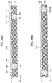
- FIG. 1 is a diagram illustrating a layout of a wiring board according to a first embodiment
- FIG. 2 is a diagram, on an enlarged scale, illustrating a micro-wiring region and a vicinity thereof in FIG. 1 ;
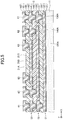
- FIG. 3 is a cross sectional diagram schematically illustrating the wiring board according to the first embodiment
- FIG. 4 is a cross sectional view illustrating details of a thin-film layer
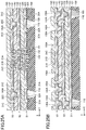
- FIG. 5 is a cross sectional view illustrating the details of the thin-film layer
- FIG. 6A and FIG. 6B are cross sectional views for explaining a method of manufacturing the wiring board according to a second embodiment
- FIG. 7A and FIG. 7B are cross sectional views for explaining the method of manufacturing the wiring board according to the second embodiment
- FIG. 8 is a cross sectional view for explaining the method of manufacturing the wiring board according to the second embodiment.
- FIG. 9A and FIG. 9B are cross sectional views for explaining the method of manufacturing the wiring board according to the second embodiment
- FIG. 10A and FIG. 10B are cross sectional views for explaining the method of manufacturing the wiring board according to the second embodiment
- FIG. 11A and FIG. 11B are cross sectional views for explaining the method of manufacturing the wiring board according to the second embodiment
- FIG. 12A and FIG. 12B are cross sectional views for explaining the method of manufacturing the wiring board according to the second embodiment
- FIG. 13A and FIG. 13B are cross sectional views for explaining the method of manufacturing the wiring board according to the second embodiment
- FIG. 14A and FIG. 14B are cross sectional views for explaining the method of manufacturing the wiring board according to the second embodiment
- FIG. 15A and FIG. 15B are cross sectional views for explaining the method of manufacturing the wiring board according to the second embodiment
- FIG. 16A and FIG. 16B are cross sectional views for explaining the method of manufacturing the wiring board according to the second embodiment
- FIG. 17A and FIG. 17B are cross sectional views for explaining the method of manufacturing the wiring board according to the second embodiment
- FIG. 18A and FIG. 18B are cross sectional views for explaining the method of manufacturing the wiring board according to the second embodiment
- FIG. 19A and FIG. 19B are cross sectional views for explaining the method of manufacturing the wiring board according to the second embodiment
- FIG. 20A and FIG. 20B are cross sectional views for explaining the method of manufacturing the wiring board according to the second embodiment
- FIG. 21A and FIG. 21B are cross sectional views for explaining the method of manufacturing the wiring board according to the second embodiment
- FIG. 22A and FIG. 22B are cross sectional views for explaining the method of manufacturing the wiring board according to the second embodiment
- FIG. 23A and FIG. 23B are cross sectional views for explaining the method of manufacturing the wiring board according to the second embodiment
- FIG. 24A and FIG. 24B are cross sectional views for explaining the method of manufacturing the wiring board according to the second embodiment
- FIG. 25A and FIG. 25B are cross sectional views for explaining the method of manufacturing the wiring board according to the second embodiment
- FIG. 26A and FIG. 26B are cross sectional views for explaining the method of manufacturing the wiring board according to the second embodiment
- FIG. 27A and FIG. 27B are cross sectional views for explaining the method of manufacturing the wiring board according to a third embodiment
- FIG. 28A and FIG. 28B are cross sectional views for explaining the method of manufacturing the wiring board according to the third embodiment
- FIG. 29A and FIG. 29B are cross sectional views for explaining the method of manufacturing the wiring board according to the third embodiment.
- FIG. 30A and FIG. 30B are cross sectional views for explaining the method of manufacturing the wiring board according to the third embodiment.
- the present inventor diligently studied to investigate the cause of the connection failure. As a result, the present inventor found that a void exists near a degassing hole that is provided in a periphery of a conductor pattern, and that peeling (or separation) of a layer is caused by this void. In addition, while the cause of the void that is generated is a micro-groove formed between the conductor patterns, the present inventor found that a groove is also formed inside the degassing hole, at the same time as the micro-groove, and that an insulating layer is not appropriately formed inside this groove.
- FIG. 1 is a diagram illustrating a layout of the wiring board according to the first embodiment.
- FIG. 2 is a diagram, on an enlarged scale, illustrating a micro-wiring region and a vicinity thereof in FIG. 1 .
- a wiring board 1 includes a first region 2 where a semiconductor integrated circuit chip, such as an Application Specific Integrated Circuit (ASIC) or the like, is mounted, and second regions 3 A, 3 B, 3 C, and 3 D where a semiconductor memory chip, such as a High Bandwidth Memory (HBM) or the like, is mounted.
- the first region 2 has a rectangular planar shape.
- the second regions 3 A and 3 B are arranged side by side along one side 5 of the first region 2
- the second regions 3 C and 3 D are arranged side by side along another side 6 of the first region 2 , parallel to the side 5 .
- a direction in which the side 5 and the side 6 extend will be referred to as a Y-direction
- a direction perpendicular to the Y-direction on a plane parallel to a principal plane of the wiring board 1 will be referred to as a X-direction.
- a micro-wiring region 4 A is provided between the first region 2 and the second region 3 A.
- the micro-wiring region 4 A includes a plurality of micro-wirings electrically connecting the semiconductor integrated circuit chip that is mounted in the first region 2 , and the semiconductor memory chip that is mounted in the second region 3 A.
- a micro-wiring region 4 B is provided between the first region 2 and the second region 3 B.
- the micro-wiring region 4 B includes a plurality of micro-wirings electrically connecting the semiconductor integrated circuit chip that is mounted in the first region 2 , and the semiconductor memory chip that is mounted in the second region 3 B.
- a micro-wiring region 4 C is provided between the first region 2 and the second region 3 C.
- the micro-wiring region 4 C includes a plurality of micro-wirings electrically connecting the semiconductor integrated circuit chip that is mounted in the first region 2 , and the semiconductor memory chip that is mounted in the second region 3 C.
- a micro-wiring region 4 D is provided between the first region 2 and the second region 3 D.
- the micro-wiring region 4 D includes a plurality of micro-wirings electrically connecting the semiconductor integrated circuit chip that is mounted in the first region 2 , and the semiconductor memory chip that is mounted in the second region 3 D.
- FIG. 2 illustrates, as an example, the micro-wiring region 4 A and a vicinity thereof, among the micro-wiring regions 4 A through 4 D.
- the micro-wiring region 4 A includes a plurality of micro-wirings 21 extending in the X-direction.
- the plurality of micro-wirings 21 are formed by a Line-and-Space (L/S) pattern in which a line width and a space width respectively are 1 ⁇ m to 5 ⁇ m, for example.
- L/S Line-and-Space
- Ground regions 7 are provided in vicinities of the first region 2 , the second regions 3 A through 3 D, and the micro-wiring regions 4 A through 4 D.
- a plurality of metal layers that are grounded, are provided in the ground region 17 .
- 3 metal layers are provided in the ground region 17 .
- a plurality of degassing holes 31 A are formed in a first metal layer, a plurality of degassing holes 31 B are faulted in a second metal layer, and a plurality of degassing holes 31 C are formed in a third metal layer.
- An anchor via pad 32 A is provided at a central part of the degassing hole 31 A
- an anchor via pad 32 B is provided at a central part of the degassing hole 31 B
- an anchor via pad 32 C is provided at a central part of the degassing hole 31 C.
- the degassing hole 31 A and the degassing hole 31 C overlap, and the anchor via pad 32 A and the anchor via pad 32 C overlap.
- the degassing hole 31 B is separated from the degassing holes 31 A and 31 C
- the anchor via pad 32 B is separated from the anchor via pads 32 A and 32 C.
- the degassing holes 31 A through 31 C have a diameter of 50 ⁇ m to 150 ⁇ m
- the anchor via pads 32 A through 32 C have a diameter of 20 ⁇ m to 40 ⁇ m.
- FIG. 3 is a cross sectional diagram schematically illustrating the wiring board according to the first embodiment.
- FIG. 4 and FIG. 5 are cross sectional views illustrating details of a thin-film layer.
- FIG. 4 corresponds to a cross sectional view along a line I-I in FIG. 2
- FIG. 5 corresponds to a cross sectional view along a line II-II in FIG. 1 .
- the wiring board 1 includes a buildup substrate 11 , and a thin-film layer 12 formed on one surface (that is, an upper surface in this example) of the buildup substrate 11 .
- the micro-wirings 21 are formed in the thin-film layer 12 .
- the surface of the buildup substrate 11 formed with the thin-film layer 12 may be referred to as a mounting side, and a surface of the buildup substrate 11 opposite to the mounting side may be referred to as a non-mounting side.
- the thin-film layer 12 includes a first micro-wiring layer 51 formed on the buildup substrate 11 , and a third insulating layer 130 covering the first micro-wiring layer 51 .
- the first micro-wiring layer 51 includes a seed layer 121 , and a metal plated layer 122 .
- the seed layer 121 includes a titanium layer, and a copper layer formed on the titanium layer, and the metal plated layer 122 is a copper plated layer.
- the first micro-wiring layer 51 includes micro-wirings 21 A, the degassing holes 31 A, and the anchor via pads 32 A.
- the micro-wirings 21 A are formed within the micro-wiring regions 4 A through 4 D, and the degassing holes 31 A and the anchor via pads 32 A are formed within the ground regions 7 .
- the micro-wirings 21 A are a part of the micro-wiring 21 .
- micro-grooves 151 are formed in the surface of the buildup substrate 11 , at a space part of the L/S pattern including the micro-wirings 21 A.
- the surface of the buildup substrate 11 is located above bottom surfaces of the micro-grooves 151 , and preferably matches an interface between the buildup substrate 11 and the micro-wirings 21 A.
- the third insulating layer 130 is formed to fill the micro-grooves 151 and the degassing holes 31 A.
- the degassing holes 31 A and the anchor via pads 32 A respectively have a circular planar shape.
- the metal plated layer 122 is an example of a metal layer
- the pattern within the micro-wiring regions 4 A through 4 D of the metal plated layer 122 is an example of a first pattern
- a pattern within the ground regions 7 of the metal plated layer 122 is an example of a second pattern.
- the micro-wirings 21 A are examples of wirings
- the micro-grooves 151 are examples of grooves.
- the thin-film layer 12 includes a second micro-wiring layer 52 formed on the third insulating layer 130 , and a fourth insulating layer 140 covering the second micro-wiring layer 52 .
- the second micro-wiring layer 52 includes a seed layer 131 , and a metal plated layer 132 .
- the seed layer 131 includes a titanium layer, and a copper layer formed on the titanium layer, and the metal plated layer 132 is a copper plated layer.
- the second micro-wiring layer 52 includes micro-wirings 21 B, the degassing holes 31 B, and the anchor via pads 32 B, as illustrated in FIG. 2 .
- the micro-wirings 21 B are formed within the micro-wiring regions 4 A through 4 D, and the degassing holes 31 B and the anchor via pads 32 B are formed within the ground regions 7 .
- the micro-wirings 21 B are a part of the micro-wiring 21 .
- micro-grooves 152 are formed in the surface of the third insulating layer 130 , at a space part of the L/S pattern including the micro-wirings 21 B.
- the surface of the third insulating layer 130 is located above bottom surfaces of the micro-grooves 152 , and preferably matches an interface between the third insulating layer 130 and the micro-wirings 21 B.
- the fourth insulating layer 140 is formed to fill the micro-grooves 152 and the degassing holes 31 B.
- the degassing holes 31 B and the anchor via pads 32 B respectively have a circular planar shape.
- the metal plated layer 132 is an example of a metal layer
- the pattern within the micro-wiring regions 4 A through 4 D of the metal plated layer 132 is an example of a first pattern
- a pattern within the ground regions 7 of the metal plated layer 132 is an example of a second pattern.
- the micro-wirings 21 B are examples of wirings
- the micro-grooves 152 are examples of grooves.
- the thin-film layer 12 includes a third micro-wiring layer 53 formed on the fourth insulating layer 140 , and a fifth insulating layer 150 covering the third micro-wiring layer 53 .
- the third micro-wiring layer 53 includes a seed layer 141 , and a metal plated layer 142 .
- the seed layer 141 includes a titanium layer, and a copper layer formed on the titanium layer, and the metal plated layer 142 is a copper plated layer.
- the third micro-wiring layer 53 includes micro-wirings 21 C, the degassing holes 31 C, and the anchor via pads 32 C.
- the micro-wirings 21 C are formed within the micro-wiring regions 4 A through 4 D, and the degassing holes 31 C and the anchor via pads 32 C are formed within the ground regions 7 .
- the micro-wirings 21 C are a part of the micro-wiring 21 .
- micro-grooves 153 are formed in the surface of the fourth insulating layer 140 , at a space part of the L/S pattern including the micro-wirings 21 C.
- the surface of the fourth insulating layer 140 is located above bottom surfaces of the micro-grooves 153 , and preferably matches an interface between the fourth insulating layer 140 and the micro-wirings 21 C.
- the fifth insulating layer 150 is formed to fill the micro-grooves 153 and the degassing holes 31 C.
- the degassing holes 31 C and the anchor via pads 32 C respectively have a circular planar shape.
- the metal plated layer 142 is an example of a metal layer
- the pattern within the micro-wiring regions 4 A through 4 D of the metal plated layer 142 is an example of a first pattern
- a pattern within the ground regions 7 of the metal plated layer 142 is an example of a second pattern.
- the micro-wirings 21 C are examples of wirings
- the micro-grooves 153 are examples of grooves.
- Micro-via holes 140 A are formed in the fourth insulating layer 140 , and the anchor via pads 32 C are joined, by metal-to-metal bonding, to the second micro-wiring layer 52 via the micro-via holes 140 A.
- micro-via holes 130 A are formed in the third insulating layer 130 , as illustrated in FIG. 5 , and the anchor via pads 32 B are joined, by metal-to-metal bonding, to the first micro-wiring layer 51 via the micro-via holes 130 A. Accordingly, the first micro-wiring layer 51 , the second micro-wiring layer 52 , and the third micro-wiring layer 53 are joined to one another, by metal-to-metal bonding, within the ground regions 7 . Consequently, a strong bonding strength can be obtained by the anchor effect.
- the thin-film layer 12 includes connection terminals 61 , 62 , and 63 that connect to end parts of the micro-wiring 21 and project from the fifth insulating layer 150 .
- the connection terminals 61 electrically connect to the micro-wirings 21 A of the first micro-wiring layer 51
- the connection terminals 62 electrically connect to the micro-wirings 21 B of the second micro-wiring layer 52
- the connection terminals 63 electrically connect to the micro-wirings 21 C of the third micro-wiring layer 53 .
- the connection terminals 61 through 63 respectively include a seed layer 161 and a metal plated layer 162 .
- the seed layer 161 includes a titanium layer, and a copper layer formed on the titanium layer
- the metal plated layer 162 is a copper plated layer.
- the micro-groove 151 is formed between the adjacent micro-wirings 21 A, to reduce ion migration between the adjacent micro-wirings 21 A.
- the micro-groove 152 is formed between the adjacent micro-wirings 21 B, to reduce ion migration between the adjacent micro-wirings 21 B, and the micro-groove 153 is formed between the adjacent micro-wirings 21 C, to reduce ion migration between the adjacent micro-wirings 21 C.
- FIG. 6A through FIG. 26B are cross sectional views for explaining the method of manufacturing the wiring board according to the second embodiment.
- This second embodiment first forms the buildup substrate 11 , and thereafter forms the thin-film layer 12 on the buildup substrate 11 .
- FIG. 6A through FIG. 8 are cross sectional views illustrating a method of forming the buildup substrate.
- FIG. 9A through FIG. 26B are cross sectional views illustrating a method of forming the thin-film layer.
- FIG. 26A illustrate a part corresponding to the cross sectional view along the line I-I in FIG. 2 .
- FIG. 9B , FIG. 10B , FIG. 11B , . . . , and FIG. 26B illustrate a part corresponding to the cross sectional view along the line II-II in FIG. 1 .
- a core wiring board 101 is prepared as a support body.
- the core wiring board 101 includes a core substrate 102 , and a first wiring layer 104 .
- the core substrate 102 includes through holes 103 A that penetrate the core substrate 102 in a thickness direction of the core substrate 102 .
- a through-conductor 103 is provided within the through hole 103 A.
- the through holes 103 A may be formed by drilling, laser beam machining, or the like.
- the through-conductor 103 and the first wiring layer 104 may be formed by plating, photolithography, or the like.
- a large board from which a plurality of wiring boards 1 can be made, may be used for the core wiring board 101 .
- the core wiring board 101 may include a plurality of regions where structures each corresponding to the wiring board 1 are formed.
- an uncured resin film is adhered on both sides (that is, both upper and lower surfaces in this example) of the core substrate 102 , and the uncured resin film is cured by performing a heat treatment, to form a first insulating layer 105 .
- the first insulating layer 105 may be formed by an insulating resin, such as epoxy resins, polyimide resins, or the like.
- the first insulating layer 105 may be formed by coating a liquid resin. Thereafter, laser beam machining is performed on the first insulating layer 105 that is provided on both sides of the core substrate 102 , to form, in the first insulating layer 105 , via holes 106 respectively reaching a connection part of the first wiring layer 104 .
- a second wiring layer 107 that electrically connects to the first wiring layer 104 through a via conductor within the via holes 106 , is formed on the first insulating layer 105 that is provided on both sides of the core substrate 102 .
- the second wiring layer 107 may be formed by a semi-additive method.
- a second insulating layer 108 is formed on the first insulating layer 105 that is provided on both sides of the core substrate 102 , as illustrated in FIG. 7B .
- the second insulating layer 108 may be formed by a method similar to that used to form the first insulating layer 105 .
- a third wiring layer 110 that electrically connects to the second wiring layer 107 through a via conductor within the via holes 109 , is formed on the second insulating layer 108 that is provided on both sides of the core substrate 102 .
- the third wiring layer 110 may be formed by a semi-additive method similar to that used to form the second wiring layer 107 .
- the third wiring layer 110 may be formed as a solid layer (or continuous layer), without forming the wiring pattern of the third wiring layer 110 on the second insulating layer 108 .
- solder resist layer 111 is formed on the second insulating layer 108 . Thereafter, openings 112 respectively reaching a connection part of the third wiring layer 110 are formed in the solder resist layer 111 .
- the solder resist layer 111 may be formed by an insulating resin, such as photosensitive epoxy resins, photosensitive acrylic resins, or the like.
- the solder resist layer 111 may be formed by adhering a resin film, or by coating a liquid resin.
- the openings 112 may be formed by exposing and developing the solder resist layer 111 .
- An insulating resin, such as non-photosensitive epoxy resins, non-photosensitive acrylic resins, or the like may be used for the solder resist layer 111 .
- the opening 112 may be formed by performing laser beam machining or blasting with respect to the non-photosensitive resin.
- the buildup substrate 11 can be formed by the processes described heretofore.
- the surface on the mounting side of the buildup substrate 11 is polished by chemical mechanical polishing, to expose the second insulating layer 108 .
- a seed layer 121 is formed on the second insulating layer 108 and the third wiring layer 110 within the via holes 109 .
- the seed layer 121 may be famed by successively forming a titanium layer and a copper layer by sputtering.
- a plated resist layer 191 including an opening at a part where the first micro-wiring layer 51 is formed, is formed on the seed layer 121 .
- the plated resist layer 191 includes openings at parts where the micro-wirings 21 A are formed and at parts where the anchor via pads 32 A are formed, and covers parts where the degassing holes 31 A are formed.
- the metal plated layer 122 made of copper or the like is formed in the openings of the plated resist layer 191 , by electroplating using the seed layer 121 as a plating power feeding path.
- the seed layer 121 is removed by wet etching, using the metal plated layer 122 as a mask.
- the micro-wirings 21 A, the degassing holes 31 A, and the anchor via pads 32 A are formed in the first micro-wiring layer 51 .
- the first micro-wiring layer 51 may be formed by a semi-additive method.
- a protection layer 181 including openings at space parts of the L/S pattern of the first micro-wiring layer 51 that includes the micro-wirings 21 A, is formed.
- the protection layer 181 may be formed by an insulating resin such as photosensitive epoxy resins or the like.
- the protection layer 181 and parts of the second insulating layer 108 exposed from the protection layer 181 , are etched.
- the micro-grooves 151 are formed in the second insulating layer 108 at the space parts of the L/S pattern that includes the micro-wirings 21 A.
- no groove is formed in parts of the second insulating layer 108 exposed through the degassing holes 31 A.
- the third insulating layer 130 including the micro-via holes 130 A above parts of the first micro-wiring layer 51 , is formed on the first micro-wiring layer 51 and the second insulating layer 108 .
- the third insulating layer 130 may be formed by an insulating resin, such as photosensitive epoxy resins or the like.
- the micro-via holes 130 A may be formed by photolithography, for example.
- the second micro-wiring layer 52 that electrically connects to the first micro-wiring layer 51 through the via conductor within the micro-via holes 130 A, is formed on the third insulating layer 130 .
- the second micro-wiring layer 52 may be formed by a semi-additive method similar to that used to form the first micro-wiring layer 51 , and includes the seed layer 131 and the metal plated layer 132 .
- the micro-wirings 21 B, the degassing holes 31 B, and the anchor via pads 32 B illustrated in FIG. 2 are formed in the second micro-wiring layer 52 .
- a protection layer 182 including openings at space parts of the L/S pattern of the second micro-wiring layer 52 that includes the micro-wirings 21 B, is formed.
- the protection layer 182 may be formed by an insulating resin such as photosensitive epoxy resins or the like.
- the protection layer 182 and parts of the third insulating layer 130 exposed from the protection layer 182 , are etched.
- the micro-grooves 152 are formed in the third insulating layer 130 at the space parts of the L/S pattern that includes the micro-wirings 21 B.
- no groove is formed in parts of the third insulating layer 130 exposed through the degassing holes 31 B.
- the fourth insulating layer 140 including the micro-via holes 140 A above parts of the second micro-wiring layer 52 , is formed on the second micro-wiring layer 52 and the third insulating layer 130 .
- the fourth insulating layer 140 may be formed by an insulating resin, such as photosensitive epoxy resins or the like.
- the micro-via holes 140 A may be formed by photolithography, for example.
- the third micro-wiring layer 53 that electrically connects to the second micro-wiring layer 52 through the via conductor within the micro-via holes 140 A, is formed on the fourth insulating layer 140 .
- the third micro-wiring layer 53 may be formed by a semi-additive method similar to that used to form the first micro-wiring layer 51 , and includes the seed layer 141 and the metal plated layer 142 .
- the micro-wirings 21 C, the degassing holes 31 C, and the anchor via pads 32 C are formed in the third micro-wiring layer 53 .
- a protection layer 183 including openings at space parts of the L/S pattern of the third micro-wiring layer 53 that includes the micro-wirings 21 C, is formed.
- the protection layer 183 may be formed by an insulating resin such as photosensitive epoxy resins or the like.
- the protection layer 183 and parts of the fourth insulating layer 140 exposed from the protection layer 183 , are etched. As a result, the micro-grooves 153 are formed in the fourth insulating layer 140 at the space parts of the L/S pattern that includes the micro-wirings 21 C. On the other hand, due to the coverage provided by the protection layer 183 , no groove is formed in parts of the fourth insulating layer 140 exposed through the degassing holes 31 C.
- the fifth insulating layer 150 including the micro-via holes 150 A above parts of the third micro-wiring layer 53 , is formed on the third micro-wiring layer 53 and the fourth insulating layer 140 .
- the fifth insulating layer 150 may be formed by an insulating resin, such as photosensitive epoxy resins or the like.
- the micro-via holes 150 A may be formed by photolithography, for example.
- connection terminals 61 through 63 that electrically connect to the third micro-wiring layer 53 through the via conductor within the micro-via holes 150 A, are formed on the fifth insulating layer 150 .
- the connection terminals 61 through 63 may be formed by a semi-additive method similar to that used to form the first micro-wiring layer 51 , and respectively include the seed layer 161 and the metal plated layer 162 .
- FIG. 26A and FIG. 26B is cut along cutting lines (not illustrated) using a slicer or the like.
- the structure is cut into a plurality of pieces respectively corresponding to the wiring board 1 , and a plurality of wiring boards 1 according to the first embodiment are obtained from the large core wiring board 101 .
- the wiring board 1 according to the first embodiment can be manufactured by the processes described heretofore.
- no groove is famed inside the degassing holes 31 A, because the micro-grooves 151 are formed in a state where the degassing holes 31 A are covered by the protection layer 181 .
- the micro-grooves 151 and the degassing holes 31 A can be appropriately filled with the third insulating layer 130 , to prevent the generation of voids.
- no groove is formed inside the degassing holes 31 B, because the micro-grooves 152 are formed in a state where the degassing holes 31 B are covered by the protection layer 182 .
- the micro-grooves 152 and the degassing holes 31 B can be appropriately filled with the fourth insulating layer 140 , to prevent the generation of voids.
- no groove is formed inside the degassing holes 31 C, because the micro-grooves 153 are formed in a state where the degassing holes 31 C are covered by the protection layer 183 .
- the micro-grooves 153 and the degassing holes 31 C can be appropriately filled with the fifth insulating layer 150 , to prevent the generation of voids. Accordingly, it is possible to reduce the peeling of the layer caused by the void, and reduce the connection failure associated with the peeling.
- FIG. 27A through FIG. 30B are cross sectional views for explaining the method of manufacturing the wiring board according to the third embodiment.
- the processes up to removal of the plated resist layer 191 are performed, similar to the second embodiment.
- the protection layer 181 is formed without removing the seed layer 121 .
- the seed layer 121 is removed by wet etching, using the metal plated layer 122 exposed from the protection layer 181 as a mask.
- the protection layer 181 and parts of the second insulating layer 108 exposed from the protection layer 181 , are etched.
- the micro-grooves 151 are formed in the second insulating layer 108 at the space parts of the L/S pattern that includes the micro-wirings 21 A.
- the coverage provided by the protection layer 181 and because the seed layer 121 remains, no groove is formed in parts of the second insulating layer 108 inside the degassing holes 31 A.
- the seed layer 121 is removed by wet etching, using the metal plated layer 122 as a mask.
- the micro-wirings 21 A, the degassing holes 31 A, and the anchor via pads 32 A are formed in the first micro-wiring layer 51 .
- the cross section illustrated in FIG. 30B remains unchanged from the cross section illustrated in FIG. 29B .
- the micro-grooves 151 are formed in a state where the seed layer 121 remains inside the degassing holes 31 A. Hence, it is possible to more positively prevent a groove from being formed in the second insulating layer 108 inside the degassing holes 31 A.
- the second micro-wiring layer 52 and the third micro-wiring layer 53 are formed by repeating similar processes.
- the micro-grooves 152 are formed in a state where the seed layer 131 remains inside the degassing holes 31 B
- the micro-grooves 153 are formed in a state where the seed layer 141 remains inside the degassing holes 31 C.
- the fifth insulating layer 150 , the connection terminals 61 through 63 , or the like are formed, and the cutting is performed using the slicer or the like.
- the structure is cut into a plurality of pieces respectively corresponding to the wiring board 1 , and a plurality of wiring boards 1 according to the first embodiment are obtained from the large core wiring board 101 .
- the wiring board 1 according to the first embodiment can be manufactured by the processes described heretofore.
- the third embodiment it is also possible to reduce the peeling of the layer caused by the void, and reduce the connection failure associated with the peeling.
- a method of manufacturing a wiring board comprising:
Landscapes
- Engineering & Computer Science (AREA)
- Manufacturing & Machinery (AREA)
- Microelectronics & Electronic Packaging (AREA)
- Production Of Multi-Layered Print Wiring Board (AREA)
- Ceramic Engineering (AREA)
- Physics & Mathematics (AREA)
- Geometry (AREA)
- Structure Of Printed Boards (AREA)
Abstract
Description
- This application is based upon and claims priority to Japanese Patent Application No. 2018-248298, filed on Dec. 28, 2018, the entire contents of which are incorporated herein by reference.
- Certain aspects of the embodiments discussed herein are related to a wiring board, and a method of manufacturing the wiring board.
- A wiring board including a cavity formed between adjacent conductor patterns, to reduce ion migration between the adjacent conductor patterns, is described in Japanese Laid-Open Patent Publication No. 2016-051834, for example.
- However, in the wiring board including the cavity formed between the adjacent conductor patterns, a connection failure may occur due to the cavity.
- Accordingly, it is an object in one aspect of the embodiments to provide a wiring board and a method of manufacturing the wiring board, which can reduce the connection failure.
- According to one aspect of the embodiments, a wiring board includes an insulating layer; and a metal layer, formed on the insulating layer, and including a first pattern that includes a plurality of wirings extending parallel to each other, and a second pattern that includes a degassing hole, wherein the insulating layer includes a groove exposed between the plurality of wirings, and wherein a surface of the insulating layer inside the degassing hole is located above a bottom surface of the groove.
- The object and advantages of the embodiments will be realized and attained by means of the elements and combinations particularly pointed out in the claims.
- It is to be understood that both the foregoing general description and the following detailed description are exemplary and explanatory and not restrictive of the invention, as claimed.
-
FIG. 1 is a diagram illustrating a layout of a wiring board according to a first embodiment; -
FIG. 2 is a diagram, on an enlarged scale, illustrating a micro-wiring region and a vicinity thereof inFIG. 1 ; -
FIG. 3 is a cross sectional diagram schematically illustrating the wiring board according to the first embodiment; -
FIG. 4 is a cross sectional view illustrating details of a thin-film layer; -
FIG. 5 is a cross sectional view illustrating the details of the thin-film layer; -
FIG. 6A andFIG. 6B are cross sectional views for explaining a method of manufacturing the wiring board according to a second embodiment; -
FIG. 7A andFIG. 7B are cross sectional views for explaining the method of manufacturing the wiring board according to the second embodiment; -
FIG. 8 is a cross sectional view for explaining the method of manufacturing the wiring board according to the second embodiment; -
FIG. 9A andFIG. 9B are cross sectional views for explaining the method of manufacturing the wiring board according to the second embodiment; -
FIG. 10A andFIG. 10B are cross sectional views for explaining the method of manufacturing the wiring board according to the second embodiment; -
FIG. 11A andFIG. 11B are cross sectional views for explaining the method of manufacturing the wiring board according to the second embodiment; -
FIG. 12A andFIG. 12B are cross sectional views for explaining the method of manufacturing the wiring board according to the second embodiment; -
FIG. 13A andFIG. 13B are cross sectional views for explaining the method of manufacturing the wiring board according to the second embodiment; -
FIG. 14A andFIG. 14B are cross sectional views for explaining the method of manufacturing the wiring board according to the second embodiment; -
FIG. 15A andFIG. 15B are cross sectional views for explaining the method of manufacturing the wiring board according to the second embodiment; -
FIG. 16A andFIG. 16B are cross sectional views for explaining the method of manufacturing the wiring board according to the second embodiment; -
FIG. 17A andFIG. 17B are cross sectional views for explaining the method of manufacturing the wiring board according to the second embodiment; -
FIG. 18A andFIG. 18B are cross sectional views for explaining the method of manufacturing the wiring board according to the second embodiment; -
FIG. 19A andFIG. 19B are cross sectional views for explaining the method of manufacturing the wiring board according to the second embodiment; -
FIG. 20A andFIG. 20B are cross sectional views for explaining the method of manufacturing the wiring board according to the second embodiment; -
FIG. 21A andFIG. 21B are cross sectional views for explaining the method of manufacturing the wiring board according to the second embodiment; -
FIG. 22A andFIG. 22B are cross sectional views for explaining the method of manufacturing the wiring board according to the second embodiment; -
FIG. 23A andFIG. 23B are cross sectional views for explaining the method of manufacturing the wiring board according to the second embodiment; -
FIG. 24A andFIG. 24B are cross sectional views for explaining the method of manufacturing the wiring board according to the second embodiment; -
FIG. 25A andFIG. 25B are cross sectional views for explaining the method of manufacturing the wiring board according to the second embodiment; -
FIG. 26A andFIG. 26B are cross sectional views for explaining the method of manufacturing the wiring board according to the second embodiment; -
FIG. 27A andFIG. 27B are cross sectional views for explaining the method of manufacturing the wiring board according to a third embodiment; -
FIG. 28A andFIG. 28B are cross sectional views for explaining the method of manufacturing the wiring board according to the third embodiment; -
FIG. 29A andFIG. 29B are cross sectional views for explaining the method of manufacturing the wiring board according to the third embodiment; and -
FIG. 30A andFIG. 30B are cross sectional views for explaining the method of manufacturing the wiring board according to the third embodiment. - The present inventor diligently studied to investigate the cause of the connection failure. As a result, the present inventor found that a void exists near a degassing hole that is provided in a periphery of a conductor pattern, and that peeling (or separation) of a layer is caused by this void. In addition, while the cause of the void that is generated is a micro-groove formed between the conductor patterns, the present inventor found that a groove is also formed inside the degassing hole, at the same time as the micro-groove, and that an insulating layer is not appropriately formed inside this groove.
- Preferred embodiments of the present invention will be described with reference to the accompanying drawings. In the drawings, those parts that are the same are designated by the same reference numerals, and a repeated description of the same parts may be omitted.
- A description will now be given of a wiring board and a method of manufacturing the wiring board in each embodiment according to the present invention.
- A first embodiment will be described. This first embodiment relates to the wiring board.
FIG. 1 is a diagram illustrating a layout of the wiring board according to the first embodiment.FIG. 2 is a diagram, on an enlarged scale, illustrating a micro-wiring region and a vicinity thereof inFIG. 1 . - As illustrated in
FIG. 1 , awiring board 1 according to the first embodiment includes afirst region 2 where a semiconductor integrated circuit chip, such as an Application Specific Integrated Circuit (ASIC) or the like, is mounted, andsecond regions first region 2 has a rectangular planar shape. Thesecond regions side 5 of thefirst region 2, and thesecond regions side 6 of thefirst region 2, parallel to theside 5. In the following description, a direction in which theside 5 and theside 6 extend will be referred to as a Y-direction, and a direction perpendicular to the Y-direction on a plane parallel to a principal plane of thewiring board 1 will be referred to as a X-direction. - A
micro-wiring region 4A is provided between thefirst region 2 and thesecond region 3A. Themicro-wiring region 4A includes a plurality of micro-wirings electrically connecting the semiconductor integrated circuit chip that is mounted in thefirst region 2, and the semiconductor memory chip that is mounted in thesecond region 3A. Amicro-wiring region 4B is provided between thefirst region 2 and thesecond region 3B. Themicro-wiring region 4B includes a plurality of micro-wirings electrically connecting the semiconductor integrated circuit chip that is mounted in thefirst region 2, and the semiconductor memory chip that is mounted in thesecond region 3B. Amicro-wiring region 4C is provided between thefirst region 2 and thesecond region 3C. Themicro-wiring region 4C includes a plurality of micro-wirings electrically connecting the semiconductor integrated circuit chip that is mounted in thefirst region 2, and the semiconductor memory chip that is mounted in thesecond region 3C. Amicro-wiring region 4D is provided between thefirst region 2 and thesecond region 3D. Themicro-wiring region 4D includes a plurality of micro-wirings electrically connecting the semiconductor integrated circuit chip that is mounted in thefirst region 2, and the semiconductor memory chip that is mounted in thesecond region 3D. -
FIG. 2 illustrates, as an example, themicro-wiring region 4A and a vicinity thereof, among themicro-wiring regions 4A through 4D. As illustrated inFIG. 2 , themicro-wiring region 4A includes a plurality ofmicro-wirings 21 extending in the X-direction. The plurality ofmicro-wirings 21 are formed by a Line-and-Space (L/S) pattern in which a line width and a space width respectively are 1 μm to 5 μm, for example. -
Ground regions 7 are provided in vicinities of thefirst region 2, thesecond regions 3A through 3D, and themicro-wiring regions 4A through 4D. A plurality of metal layers that are grounded, are provided in the ground region 17. In this example, 3 metal layers are provided in the ground region 17. A plurality ofdegassing holes 31A are formed in a first metal layer, a plurality of degassingholes 31B are faulted in a second metal layer, and a plurality ofdegassing holes 31C are formed in a third metal layer. An anchor viapad 32A is provided at a central part of thedegassing hole 31A, an anchor viapad 32B is provided at a central part of thedegassing hole 31B, and an anchor viapad 32C is provided at a central part of thedegassing hole 31C. In a plan view, thedegassing hole 31A and thedegassing hole 31C overlap, and the anchor viapad 32A and the anchor viapad 32C overlap. In the plan view, thedegassing hole 31B is separated from thedegassing holes pad 32B is separated from the anchor viapads pads 32A through 32C have a diameter of 20 μm to 40 μm. - Next, a cross sectional structure of the wiring board will be described.
FIG. 3 is a cross sectional diagram schematically illustrating the wiring board according to the first embodiment.FIG. 4 andFIG. 5 are cross sectional views illustrating details of a thin-film layer.FIG. 4 corresponds to a cross sectional view along a line I-I inFIG. 2 , andFIG. 5 corresponds to a cross sectional view along a line II-II inFIG. 1 . - As illustrated in
FIG. 3 , thewiring board 1 includes abuildup substrate 11, and a thin-film layer 12 formed on one surface (that is, an upper surface in this example) of thebuildup substrate 11. The micro-wirings 21 are formed in the thin-film layer 12. In the following description, the surface of thebuildup substrate 11 formed with the thin-film layer 12 may be referred to as a mounting side, and a surface of thebuildup substrate 11 opposite to the mounting side may be referred to as a non-mounting side. - As illustrated in
FIG. 4 , the thin-film layer 12 includes a firstmicro-wiring layer 51 formed on thebuildup substrate 11, and a thirdinsulating layer 130 covering the firstmicro-wiring layer 51. The firstmicro-wiring layer 51 includes aseed layer 121, and a metal platedlayer 122. For example, theseed layer 121 includes a titanium layer, and a copper layer formed on the titanium layer, and the metal platedlayer 122 is a copper plated layer. The firstmicro-wiring layer 51 includes micro-wirings 21A, the degassing holes 31A, and the anchor viapads 32A. The micro-wirings 21A are formed within themicro-wiring regions 4A through 4D, and thedegassing holes 31A and the anchor viapads 32A are formed within theground regions 7. The micro-wirings 21A are a part of the micro-wiring 21. In addition, micro-grooves 151 are formed in the surface of thebuildup substrate 11, at a space part of the L/S pattern including the micro-wirings 21A. On the other hand, inside the degassing holes 31A, the surface of thebuildup substrate 11 is located above bottom surfaces of the micro-grooves 151, and preferably matches an interface between thebuildup substrate 11 and the micro-wirings 21A. The thirdinsulating layer 130 is formed to fill themicro-grooves 151 and thedegassing holes 31A. For example, thedegassing holes 31A and the anchor viapads 32A respectively have a circular planar shape. The metal platedlayer 122 is an example of a metal layer, the pattern within themicro-wiring regions 4A through 4D of the metal platedlayer 122 is an example of a first pattern, and a pattern within theground regions 7 of the metal platedlayer 122 is an example of a second pattern. The micro-wirings 21A are examples of wirings, and themicro-grooves 151 are examples of grooves. - The thin-
film layer 12 includes a secondmicro-wiring layer 52 formed on the third insulatinglayer 130, and a fourth insulatinglayer 140 covering the secondmicro-wiring layer 52. The secondmicro-wiring layer 52 includes aseed layer 131, and a metal platedlayer 132. For example, theseed layer 131 includes a titanium layer, and a copper layer formed on the titanium layer, and the metal platedlayer 132 is a copper plated layer. The secondmicro-wiring layer 52 includes micro-wirings 21B, the degassing holes 31B, and the anchor viapads 32B, as illustrated inFIG. 2 . The micro-wirings 21B are formed within themicro-wiring regions 4A through 4D, and the degassing holes 31B and the anchor viapads 32B are formed within theground regions 7. The micro-wirings 21B are a part of the micro-wiring 21. In addition, micro-grooves 152 are formed in the surface of the third insulatinglayer 130, at a space part of the L/S pattern including the micro-wirings 21B. On the other hand, inside the degassing holes 31B, the surface of the third insulatinglayer 130 is located above bottom surfaces of the micro-grooves 152, and preferably matches an interface between the third insulatinglayer 130 and the micro-wirings 21B. The fourth insulatinglayer 140 is formed to fill themicro-grooves 152 and the degassing holes 31B. For example, the degassing holes 31B and the anchor viapads 32B respectively have a circular planar shape. The metal platedlayer 132 is an example of a metal layer, the pattern within themicro-wiring regions 4A through 4D of the metal platedlayer 132 is an example of a first pattern, and a pattern within theground regions 7 of the metal platedlayer 132 is an example of a second pattern. The micro-wirings 21B are examples of wirings, and themicro-grooves 152 are examples of grooves. - The thin-
film layer 12 includes a thirdmicro-wiring layer 53 formed on the fourth insulatinglayer 140, and a fifth insulatinglayer 150 covering the thirdmicro-wiring layer 53. The thirdmicro-wiring layer 53 includes aseed layer 141, and a metal platedlayer 142. For example, theseed layer 141 includes a titanium layer, and a copper layer formed on the titanium layer, and the metal platedlayer 142 is a copper plated layer. The thirdmicro-wiring layer 53 includes micro-wirings 21C, the degassing holes 31C, and the anchor viapads 32C. The micro-wirings 21C are formed within themicro-wiring regions 4A through 4D, and thedegassing holes 31C and the anchor viapads 32C are formed within theground regions 7. The micro-wirings 21C are a part of the micro-wiring 21. In addition, micro-grooves 153 are formed in the surface of the fourth insulatinglayer 140, at a space part of the L/S pattern including the micro-wirings 21C. On the other hand, inside the degassing holes 31C, the surface of the fourth insulatinglayer 140 is located above bottom surfaces of the micro-grooves 153, and preferably matches an interface between the fourth insulatinglayer 140 and the micro-wirings 21C. The fifth insulatinglayer 150 is formed to fill themicro-grooves 153 and the degassing holes 31C. For example, thedegassing holes 31C and the anchor viapads 32C respectively have a circular planar shape. The metal platedlayer 142 is an example of a metal layer, the pattern within themicro-wiring regions 4A through 4D of the metal platedlayer 142 is an example of a first pattern, and a pattern within theground regions 7 of the metal platedlayer 142 is an example of a second pattern. The micro-wirings 21C are examples of wirings, and themicro-grooves 153 are examples of grooves. - Micro-via holes 140A are formed in the fourth insulating
layer 140, and the anchor viapads 32C are joined, by metal-to-metal bonding, to the secondmicro-wiring layer 52 via the micro-via holes 140A. In addition,micro-via holes 130A are formed in the third insulatinglayer 130, as illustrated inFIG. 5 , and the anchor viapads 32B are joined, by metal-to-metal bonding, to the firstmicro-wiring layer 51 via the micro-via holes 130A. Accordingly, the firstmicro-wiring layer 51, the secondmicro-wiring layer 52, and the thirdmicro-wiring layer 53 are joined to one another, by metal-to-metal bonding, within theground regions 7. Consequently, a strong bonding strength can be obtained by the anchor effect. - As illustrated in
FIG. 5 , the thin-film layer 12 includesconnection terminals layer 150. Theconnection terminals 61 electrically connect to the micro-wirings 21A of the firstmicro-wiring layer 51, theconnection terminals 62 electrically connect to the micro-wirings 21B of the secondmicro-wiring layer 52, and theconnection terminals 63 electrically connect to the micro-wirings 21C of the thirdmicro-wiring layer 53. Theconnection terminals 61 through 63 respectively include aseed layer 161 and a metal platedlayer 162. For example, theseed layer 161 includes a titanium layer, and a copper layer formed on the titanium layer, and the metal platedlayer 162 is a copper plated layer. - According to the
wiring board 1, the micro-groove 151 is formed between the adjacent micro-wirings 21A, to reduce ion migration between the adjacent micro-wirings 21A. Similarly, the micro-groove 152 is formed between the adjacent micro-wirings 21B, to reduce ion migration between the adjacent micro-wirings 21B, and the micro-groove 153 is formed between the adjacent micro-wirings 21C, to reduce ion migration between the adjacent micro-wirings 21C. - Further, since no groove is formed inside each of the degassing holes 31A through 31C, voids are uneasily generated in the third insulating
layer 130, the fourth insulatinglayer 140, and the fifth insulatinglayer 150. Hence, it is possible to reduce peeling (or separation) of the layer within the thin-film layer 12, and reduce the connection failure associated with the peeling. - Next, a second embodiment will be described. This second embodiment relates to a method of manufacturing the
wiring board 1 according to the first embodiment.FIG. 6A throughFIG. 26B are cross sectional views for explaining the method of manufacturing the wiring board according to the second embodiment. This second embodiment first forms thebuildup substrate 11, and thereafter forms the thin-film layer 12 on thebuildup substrate 11.FIG. 6A throughFIG. 8 are cross sectional views illustrating a method of forming the buildup substrate.FIG. 9A throughFIG. 26B are cross sectional views illustrating a method of forming the thin-film layer.FIG. 9A ,FIG. 10A ,FIG. 11A , . . . , andFIG. 26A illustrate a part corresponding to the cross sectional view along the line I-I inFIG. 2 .FIG. 9B ,FIG. 10B ,FIG. 11B , . . . , andFIG. 26B illustrate a part corresponding to the cross sectional view along the line II-II inFIG. 1 . - First, as illustrated in
FIG. 6A , acore wiring board 101 is prepared as a support body. Thecore wiring board 101 includes acore substrate 102, and afirst wiring layer 104. Thecore substrate 102 includes throughholes 103A that penetrate thecore substrate 102 in a thickness direction of thecore substrate 102. A through-conductor 103 is provided within the throughhole 103A. For example, the throughholes 103A may be formed by drilling, laser beam machining, or the like. For example, the through-conductor 103 and thefirst wiring layer 104 may be formed by plating, photolithography, or the like. A large board from which a plurality ofwiring boards 1 can be made, may be used for thecore wiring board 101. In other words, thecore wiring board 101 may include a plurality of regions where structures each corresponding to thewiring board 1 are formed. - Next, as illustrated in
FIG. 6B , an uncured resin film is adhered on both sides (that is, both upper and lower surfaces in this example) of thecore substrate 102, and the uncured resin film is cured by performing a heat treatment, to form a first insulatinglayer 105. The first insulatinglayer 105 may be formed by an insulating resin, such as epoxy resins, polyimide resins, or the like. The first insulatinglayer 105 may be formed by coating a liquid resin. Thereafter, laser beam machining is performed on the first insulatinglayer 105 that is provided on both sides of thecore substrate 102, to form, in the first insulatinglayer 105, viaholes 106 respectively reaching a connection part of thefirst wiring layer 104. - Next, as illustrated in
FIG. 7A , asecond wiring layer 107, that electrically connects to thefirst wiring layer 104 through a via conductor within the via holes 106, is formed on the first insulatinglayer 105 that is provided on both sides of thecore substrate 102. Thesecond wiring layer 107 may be formed by a semi-additive method. - After forming the
second wiring layer 107, a second insulatinglayer 108, including viaholes 109 at a connection part of thesecond wiring layer 107, is formed on the first insulatinglayer 105 that is provided on both sides of thecore substrate 102, as illustrated inFIG. 7B . The secondinsulating layer 108 may be formed by a method similar to that used to form the first insulatinglayer 105. - Further, as also illustrated in
FIG. 7B , athird wiring layer 110, that electrically connects to thesecond wiring layer 107 through a via conductor within the via holes 109, is formed on the second insulatinglayer 108 that is provided on both sides of thecore substrate 102. Thethird wiring layer 110 may be formed by a semi-additive method similar to that used to form thesecond wiring layer 107. However, on the mounting side of thecore substrate 102, thethird wiring layer 110 may be formed as a solid layer (or continuous layer), without forming the wiring pattern of thethird wiring layer 110 on the second insulatinglayer 108. - Next, as illustrated in
FIG. 8 , on the non-mounting side of thecore substrate 102, a solder resistlayer 111 is formed on the second insulatinglayer 108. Thereafter,openings 112 respectively reaching a connection part of thethird wiring layer 110 are formed in the solder resistlayer 111. - The solder resist
layer 111 may be formed by an insulating resin, such as photosensitive epoxy resins, photosensitive acrylic resins, or the like. The solder resistlayer 111 may be formed by adhering a resin film, or by coating a liquid resin. Theopenings 112 may be formed by exposing and developing the solder resistlayer 111. An insulating resin, such as non-photosensitive epoxy resins, non-photosensitive acrylic resins, or the like may be used for the solder resistlayer 111. In this case, theopening 112 may be formed by performing laser beam machining or blasting with respect to the non-photosensitive resin. - The
buildup substrate 11 can be formed by the processes described heretofore. - Next, as illustrated in
FIG. 9A andFIG. 9B , the surface on the mounting side of thebuildup substrate 11 is polished by chemical mechanical polishing, to expose the second insulatinglayer 108. - Thereafter, as illustrated in
FIG. 10A and FIG. 10B, aseed layer 121 is formed on the second insulatinglayer 108 and thethird wiring layer 110 within the via holes 109. For example, theseed layer 121 may be famed by successively forming a titanium layer and a copper layer by sputtering. - Next, as illustrated in
FIG. 11A andFIG. 11B , a plated resistlayer 191, including an opening at a part where the firstmicro-wiring layer 51 is formed, is formed on theseed layer 121. For example, the plated resistlayer 191 includes openings at parts where the micro-wirings 21A are formed and at parts where the anchor viapads 32A are formed, and covers parts where the degassing holes 31A are formed. - Next, as illustrated in
FIG. 12A andFIG. 12B , the metal platedlayer 122 made of copper or the like is formed in the openings of the plated resistlayer 191, by electroplating using theseed layer 121 as a plating power feeding path. - Thereafter, as illustrated in
FIG. 13A andFIG. 13B , the plated resistlayer 191 is removed. - Next, as illustrated in
FIG. 14A andFIG. 14B , theseed layer 121 is removed by wet etching, using the metal platedlayer 122 as a mask. The micro-wirings 21A, the degassing holes 31A, and the anchor viapads 32A are formed in the firstmicro-wiring layer 51. Hence, the firstmicro-wiring layer 51 may be formed by a semi-additive method. - Next, as illustrated in
FIG. 15A andFIG. 15B , aprotection layer 181, including openings at space parts of the L/S pattern of the firstmicro-wiring layer 51 that includes the micro-wirings 21A, is formed. For example, theprotection layer 181 may be formed by an insulating resin such as photosensitive epoxy resins or the like. - Thereafter, as illustrated in
FIG. 16A andFIG. 16B , theprotection layer 181, and parts of the second insulatinglayer 108 exposed from theprotection layer 181, are etched. As a result, the micro-grooves 151 are formed in the second insulatinglayer 108 at the space parts of the L/S pattern that includes the micro-wirings 21A. On the other hand, due to the coverage provided by theprotection layer 181, no groove is formed in parts of the second insulatinglayer 108 exposed through thedegassing holes 31A. - Next, as illustrated in
FIG. 17A andFIG. 17B , the third insulatinglayer 130, including themicro-via holes 130A above parts of the firstmicro-wiring layer 51, is formed on the firstmicro-wiring layer 51 and the second insulatinglayer 108. For example, the third insulatinglayer 130 may be formed by an insulating resin, such as photosensitive epoxy resins or the like. The micro-via holes 130A may be formed by photolithography, for example. - Next, as illustrated in
FIG. 18A andFIG. 18B , the secondmicro-wiring layer 52, that electrically connects to the firstmicro-wiring layer 51 through the via conductor within the micro-via holes 130A, is formed on the third insulatinglayer 130. The secondmicro-wiring layer 52 may be formed by a semi-additive method similar to that used to form the firstmicro-wiring layer 51, and includes theseed layer 131 and the metal platedlayer 132. The micro-wirings 21B, the degassing holes 31B, and the anchor viapads 32B illustrated inFIG. 2 are formed in the secondmicro-wiring layer 52. - Thereafter, as illustrated in
FIG. 19A andFIG. 19B , aprotection layer 182, including openings at space parts of the L/S pattern of the secondmicro-wiring layer 52 that includes the micro-wirings 21B, is formed. For example, theprotection layer 182 may be formed by an insulating resin such as photosensitive epoxy resins or the like. - Next, as illustrated in
FIG. 20A andFIG. 20B , theprotection layer 182, and parts of the third insulatinglayer 130 exposed from theprotection layer 182, are etched. As a result, the micro-grooves 152 are formed in the third insulatinglayer 130 at the space parts of the L/S pattern that includes the micro-wirings 21B. On the other hand, due to the coverage provided by theprotection layer 182, no groove is formed in parts of the third insulatinglayer 130 exposed through the degassing holes 31B. - Next, as illustrated in
FIG. 21A andFIG. 21B , the fourth insulatinglayer 140, including themicro-via holes 140A above parts of the secondmicro-wiring layer 52, is formed on the secondmicro-wiring layer 52 and the third insulatinglayer 130. For example, the fourth insulatinglayer 140 may be formed by an insulating resin, such as photosensitive epoxy resins or the like. The micro-via holes 140A may be formed by photolithography, for example. - Thereafter, as illustrated in
FIG. 22A andFIG. 22B , the thirdmicro-wiring layer 53, that electrically connects to the secondmicro-wiring layer 52 through the via conductor within the micro-via holes 140A, is formed on the fourth insulatinglayer 140. The thirdmicro-wiring layer 53 may be formed by a semi-additive method similar to that used to form the firstmicro-wiring layer 51, and includes theseed layer 141 and the metal platedlayer 142. The micro-wirings 21C, the degassing holes 31C, and the anchor viapads 32C are formed in the thirdmicro-wiring layer 53. - Next, as illustrated in
FIG. 23A andFIG. 23B , aprotection layer 183, including openings at space parts of the L/S pattern of the thirdmicro-wiring layer 53 that includes the micro-wirings 21C, is formed. For example, theprotection layer 183 may be formed by an insulating resin such as photosensitive epoxy resins or the like. - Next, as illustrated in
FIG. 24A andFIG. 24B , theprotection layer 183, and parts of the fourth insulatinglayer 140 exposed from theprotection layer 183, are etched. As a result, the micro-grooves 153 are formed in the fourth insulatinglayer 140 at the space parts of the L/S pattern that includes the micro-wirings 21C. On the other hand, due to the coverage provided by theprotection layer 183, no groove is formed in parts of the fourth insulatinglayer 140 exposed through the degassing holes 31C. - Thereafter, as illustrated in
FIG. 25A andFIG. 25B , the fifth insulatinglayer 150, including themicro-via holes 150A above parts of the thirdmicro-wiring layer 53, is formed on the thirdmicro-wiring layer 53 and the fourth insulatinglayer 140. For example, the fifth insulatinglayer 150 may be formed by an insulating resin, such as photosensitive epoxy resins or the like. The micro-via holes 150A may be formed by photolithography, for example. - Next, as illustrated in
FIG. 26A andFIG. 26B , theconnection terminals 61 through 63, that electrically connect to the thirdmicro-wiring layer 53 through the via conductor within the micro-via holes 150A, are formed on the fifth insulatinglayer 150. Theconnection terminals 61 through 63 may be formed by a semi-additive method similar to that used to form the firstmicro-wiring layer 51, and respectively include theseed layer 161 and the metal platedlayer 162. - Next, the structure illustrated in
FIG. 26A andFIG. 26B is cut along cutting lines (not illustrated) using a slicer or the like. Hence, the structure is cut into a plurality of pieces respectively corresponding to thewiring board 1, and a plurality ofwiring boards 1 according to the first embodiment are obtained from the largecore wiring board 101. Thewiring board 1 according to the first embodiment can be manufactured by the processes described heretofore. - According to this manufacturing method, no groove is famed inside the degassing holes 31A, because the micro-grooves 151 are formed in a state where the degassing holes 31A are covered by the
protection layer 181. For this reason, themicro-grooves 151 and thedegassing holes 31A can be appropriately filled with the third insulatinglayer 130, to prevent the generation of voids. In addition, no groove is formed inside the degassing holes 31B, because the micro-grooves 152 are formed in a state where the degassing holes 31B are covered by theprotection layer 182. For this reason, themicro-grooves 152 and the degassing holes 31B can be appropriately filled with the fourth insulatinglayer 140, to prevent the generation of voids. Further, no groove is formed inside the degassing holes 31C, because the micro-grooves 153 are formed in a state where the degassing holes 31C are covered by theprotection layer 183. For this reason, themicro-grooves 153 and the degassing holes 31C can be appropriately filled with the fifth insulatinglayer 150, to prevent the generation of voids. Accordingly, it is possible to reduce the peeling of the layer caused by the void, and reduce the connection failure associated with the peeling. - Next, a third embodiment will be described. This third embodiment relates to another method of manufacturing the
wiring board 1 according to the first embodiment. In the following, features of this third embodiment that differ from those of the second embodiment will be described.FIG. 27A throughFIG. 30B are cross sectional views for explaining the method of manufacturing the wiring board according to the third embodiment. - In this third embodiment, as illustrated in
FIG. 27A andFIG. 27B , the processes up to removal of the plated resistlayer 191 are performed, similar to the second embodiment. Next, theprotection layer 181 is formed without removing theseed layer 121. - Next, as illustrated in
FIG. 28A andFIG. 28B , theseed layer 121 is removed by wet etching, using the metal platedlayer 122 exposed from theprotection layer 181 as a mask. - Thereafter, as illustrated in
FIG. 29A andFIG. 29B , theprotection layer 181, and parts of the second insulatinglayer 108 exposed from theprotection layer 181, are etched. As a result, the micro-grooves 151 are formed in the second insulatinglayer 108 at the space parts of the L/S pattern that includes the micro-wirings 21A. On the other hand, due to the coverage provided by theprotection layer 181, and because theseed layer 121 remains, no groove is formed in parts of the second insulatinglayer 108 inside thedegassing holes 31A. - Next, as illustrated in
FIG. 30A , theseed layer 121 is removed by wet etching, using the metal platedlayer 122 as a mask. The micro-wirings 21A, the degassing holes 31A, and the anchor viapads 32A are formed in the firstmicro-wiring layer 51. The cross section illustrated inFIG. 30B remains unchanged from the cross section illustrated inFIG. 29B . - According to the third embodiment, the micro-grooves 151 are formed in a state where the
seed layer 121 remains inside thedegassing holes 31A. Hence, it is possible to more positively prevent a groove from being formed in the second insulatinglayer 108 inside thedegassing holes 31A. - Thereafter, the second
micro-wiring layer 52 and the thirdmicro-wiring layer 53 are formed by repeating similar processes. In other words, the micro-grooves 152 are formed in a state where theseed layer 131 remains inside the degassing holes 31B, and themicro-grooves 153 are formed in a state where theseed layer 141 remains inside the degassing holes 31C. - Next, the fifth insulating
layer 150, theconnection terminals 61 through 63, or the like are formed, and the cutting is performed using the slicer or the like. As a result, the structure is cut into a plurality of pieces respectively corresponding to thewiring board 1, and a plurality ofwiring boards 1 according to the first embodiment are obtained from the largecore wiring board 101. Thewiring board 1 according to the first embodiment can be manufactured by the processes described heretofore. - According to the third embodiment, it is also possible to reduce the peeling of the layer caused by the void, and reduce the connection failure associated with the peeling.
- Therefore, according to each of the embodiments described above, it is possible to reduce the connection failure.
- Although examples of preferable embodiments are described heretofore, the present invention is not limited to these embodiments, and various variations, modifications, and substitutions may be made without departing from the scope of the present invention. For example, although the described embodiments use the buildup substrate, it is of course possible to use a support substrate or a support base in place of the buildup substrate.
- Various aspects of the subject-matter described herein may be set out non-exhaustively in the following numbered clauses:
- 1. A method of manufacturing a wiring board, comprising:
- forming a metal layer on an insulating layer;
- forming, in the metal layer, a first pattern that includes a plurality of wirings extending parallel to each other, and a second pattern that includes a degassing hole; and
- forming a groove in the insulating layer, by etching the insulating layer exposed between the plurality of wirings, in a state where the second pattern is covered by a protection layer.
- 2. The method of manufacturing the wiring board according to
clause 1, further comprising: - forming a seed layer on the insulating layer, before the forming the metal layer; and
- forming a degassing hole in the seed layer, before the forming the groove.
- 3. The method of manufacturing the wiring board according to
clause 1, further comprising: - forming a seed layer on the insulating layer, before the forming the metal layer; and
- forming a degassing hole in the seed layer, after the forming the groove.
- 4. The method of manufacturing the wiring board according to any one of
clauses 1 to 3, wherein the plurality of wirings are formed by a line-and-space pattern. - 5. The method of manufacturing the wiring board according to any one of
clauses 1 to 4, wherein the degassing hole has a circular planar shape. - 6. The method of manufacturing the wiring board according to any one of
clauses 1 to 5, wherein the forming the first pattern and the second pattern includes forming a pad in the metal layer inside the degassing hole. - 7. The method of manufacturing the wiring board according to clause 4, wherein the forming the groove forms the groove in the insulating layer, at a space part of the line-and-space pattern.
- Although the embodiments are numbered with, for example, “first,” “second,” or “third,” the ordinal numbers do not imply priorities of the embodiments. Many other variations and modifications will be apparent to those skilled in the art.
- All examples and conditional language recited herein are intended for pedagogical purposes to aid the reader in understanding the invention and the concepts contributed by the inventor to furthering the art, and are to be construed as being without limitation to such specifically recited examples and conditions, nor does the organization of such examples in the specification relate to a showing of the superiority and inferiority of the invention. Although the embodiments of the present invention have been described in detail, it should be understood that the various changes, substitutions, and alterations could be made hereto without departing from the spirit and scope of the invention.
Claims (7)
Applications Claiming Priority (2)
| Application Number | Priority Date | Filing Date | Title |
|---|---|---|---|
| JP2018-248298 | 2018-12-28 | ||
| JP2018248298A JP7145068B2 (en) | 2018-12-28 | 2018-12-28 | Wiring board and its manufacturing method |
Publications (2)
| Publication Number | Publication Date |
|---|---|
| US20200211971A1 true US20200211971A1 (en) | 2020-07-02 |
| US10804210B2 US10804210B2 (en) | 2020-10-13 |
Family
ID=71124178
Family Applications (1)
| Application Number | Title | Priority Date | Filing Date |
|---|---|---|---|
| US16/710,619 Active US10804210B2 (en) | 2018-12-28 | 2019-12-11 | Wiring board |
Country Status (2)
| Country | Link |
|---|---|
| US (1) | US10804210B2 (en) |
| JP (1) | JP7145068B2 (en) |
Cited By (2)
| Publication number | Priority date | Publication date | Assignee | Title |
|---|---|---|---|---|
| WO2023023146A1 (en) * | 2021-08-19 | 2023-02-23 | Texas Instruments Incorporated | Electronic device multilevel package substrate for improved electromigration preformance |
| EP4170709A1 (en) * | 2021-10-19 | 2023-04-26 | InnoLux Corporation | Electronic device and method of fabricating electronic device |
Families Citing this family (1)
| Publication number | Priority date | Publication date | Assignee | Title |
|---|---|---|---|---|
| JP7589574B2 (en) * | 2021-02-10 | 2024-11-26 | Toppanホールディングス株式会社 | Multilayer wiring board |
Citations (12)
| Publication number | Priority date | Publication date | Assignee | Title |
|---|---|---|---|---|
| US3293353A (en) * | 1964-03-30 | 1966-12-20 | Gen Electric | Shielded interconnecting wiring medium |
| US4061263A (en) * | 1976-09-22 | 1977-12-06 | International Telephone And Telegraph Corporation | Method of bonding a dielectric substrate to a metallic carrier in a printed circuit assembly |
| US6106923A (en) * | 1997-05-20 | 2000-08-22 | Fujitsu Limited | Venting hole designs for multilayer conductor-dielectric structures |
| US6124553A (en) * | 1993-06-12 | 2000-09-26 | Hitachi, Ltd. | Multilayer wiring board having vent holes and method of making |
| US20030127249A1 (en) * | 2002-01-08 | 2003-07-10 | International Business Machines Corporation | Vents with signal image for signal return path |
| US20030146020A1 (en) * | 2002-02-04 | 2003-08-07 | Brist Gary A. | Power-ground plane partitioning and via connection to utilize channel/trenches for power delivery |
| US20030213616A1 (en) * | 2002-05-16 | 2003-11-20 | Junpei Kusukawa | Printed wiring board and electronic device using the same |
| US20080173469A1 (en) * | 2006-12-19 | 2008-07-24 | Shinko Electric Industries Co., Ltd. | Multilayer wiring board |
| US7659790B2 (en) * | 2006-08-22 | 2010-02-09 | Lecroy Corporation | High speed signal transmission line having reduced thickness regions |
| US20130256000A1 (en) * | 2012-03-30 | 2013-10-03 | Ibiden Co., Ltd. | Wiring board and method for manufacturing the same |
| US20160020163A1 (en) * | 2014-07-16 | 2016-01-21 | Shinko Electric Industries Co., Ltd. | Wiring Substrate and Semiconductor Device |
| US20160066423A1 (en) * | 2014-09-01 | 2016-03-03 | Ibiden Co., Ltd. | Printed wiring board and method for manufacturing the same |
Family Cites Families (1)
| Publication number | Priority date | Publication date | Assignee | Title |
|---|---|---|---|---|
| JP2015162528A (en) * | 2014-02-27 | 2015-09-07 | 京セラサーキットソリューションズ株式会社 | Wiring board |
-
2018
- 2018-12-28 JP JP2018248298A patent/JP7145068B2/en active Active
-
2019
- 2019-12-11 US US16/710,619 patent/US10804210B2/en active Active
Patent Citations (12)
| Publication number | Priority date | Publication date | Assignee | Title |
|---|---|---|---|---|
| US3293353A (en) * | 1964-03-30 | 1966-12-20 | Gen Electric | Shielded interconnecting wiring medium |
| US4061263A (en) * | 1976-09-22 | 1977-12-06 | International Telephone And Telegraph Corporation | Method of bonding a dielectric substrate to a metallic carrier in a printed circuit assembly |
| US6124553A (en) * | 1993-06-12 | 2000-09-26 | Hitachi, Ltd. | Multilayer wiring board having vent holes and method of making |
| US6106923A (en) * | 1997-05-20 | 2000-08-22 | Fujitsu Limited | Venting hole designs for multilayer conductor-dielectric structures |
| US20030127249A1 (en) * | 2002-01-08 | 2003-07-10 | International Business Machines Corporation | Vents with signal image for signal return path |
| US20030146020A1 (en) * | 2002-02-04 | 2003-08-07 | Brist Gary A. | Power-ground plane partitioning and via connection to utilize channel/trenches for power delivery |
| US20030213616A1 (en) * | 2002-05-16 | 2003-11-20 | Junpei Kusukawa | Printed wiring board and electronic device using the same |
| US7659790B2 (en) * | 2006-08-22 | 2010-02-09 | Lecroy Corporation | High speed signal transmission line having reduced thickness regions |
| US20080173469A1 (en) * | 2006-12-19 | 2008-07-24 | Shinko Electric Industries Co., Ltd. | Multilayer wiring board |
| US20130256000A1 (en) * | 2012-03-30 | 2013-10-03 | Ibiden Co., Ltd. | Wiring board and method for manufacturing the same |
| US20160020163A1 (en) * | 2014-07-16 | 2016-01-21 | Shinko Electric Industries Co., Ltd. | Wiring Substrate and Semiconductor Device |
| US20160066423A1 (en) * | 2014-09-01 | 2016-03-03 | Ibiden Co., Ltd. | Printed wiring board and method for manufacturing the same |
Cited By (4)
| Publication number | Priority date | Publication date | Assignee | Title |
|---|---|---|---|---|
| WO2023023146A1 (en) * | 2021-08-19 | 2023-02-23 | Texas Instruments Incorporated | Electronic device multilevel package substrate for improved electromigration preformance |
| US11978699B2 (en) | 2021-08-19 | 2024-05-07 | Texas Instruments Incorporated | Electronic device multilevel package substrate for improved electromigration preformance |
| US12400945B2 (en) | 2021-08-19 | 2025-08-26 | Texas Instruments Incorporated | Electronic device multilevel package substrate for improved electromigration performance |
| EP4170709A1 (en) * | 2021-10-19 | 2023-04-26 | InnoLux Corporation | Electronic device and method of fabricating electronic device |
Also Published As
| Publication number | Publication date |
|---|---|
| JP7145068B2 (en) | 2022-09-30 |
| US10804210B2 (en) | 2020-10-13 |
| JP2020107860A (en) | 2020-07-09 |
Similar Documents
| Publication | Publication Date | Title |
|---|---|---|
| US9420703B2 (en) | Wiring board and manufacturing method of the same | |
| US8772643B2 (en) | Multilayer wiring substrate, and method of manufacturing the same | |
| KR101811923B1 (en) | Circuit board | |
| US11289403B2 (en) | Multi-layer substrate and method for manufacturing multi-layer substrate | |
| CN103369811B (en) | Circuit card and manufacture method thereof | |
| US20140202740A1 (en) | Method of Manufacturing Multilayer Wiring Substrate, and Multilayer Wiring Substrate | |
| US8847082B2 (en) | Multilayer wiring substrate | |
| US8859077B2 (en) | Method of manufacturing multilayer wiring substrate, and multilayer wiring substrate | |
| JP6328878B2 (en) | Method for collective manufacture of a three-dimensional electronic module comprising only an activated printed circuit board | |
| JP5547615B2 (en) | WIRING BOARD, SEMICONDUCTOR DEVICE, AND WIRING BOARD MANUFACTURING METHOD | |
| KR20160026710A (en) | Wiring substrate and method for manufacturing wiring substrate | |
| US9793200B2 (en) | Printed wiring board | |
| US10804210B2 (en) | Wiring board | |
| JP5848404B2 (en) | Wiring board and manufacturing method thereof | |
| US10743403B2 (en) | Wiring board | |
| US8658905B2 (en) | Multilayer wiring substrate | |
| KR101501902B1 (en) | Printed circuit board substrate having metal post and the method of manufacturing the same | |
| US20240030144A1 (en) | Wiring substrate | |
| TWI778816B (en) | Package structure with interconnection between chips and package method thereof | |
| US12513829B2 (en) | Wiring board, semiconductor device, and wiring board manufacturing method | |
| JP6030513B2 (en) | Wiring board manufacturing method | |
| CN120727691A (en) | Wiring substrate | |
| KR20150049165A (en) | Printed circuit boards and manufacturing methods thereof |
Legal Events
| Date | Code | Title | Description |
|---|---|---|---|
| AS | Assignment |
Owner name: SHINKO ELECTRIC INDUSTRIES CO., LTD., JAPAN Free format text: ASSIGNMENT OF ASSIGNORS INTEREST;ASSIGNOR:MIZUTANI, RIE;REEL/FRAME:051249/0188 Effective date: 20191203 |
|
| FEPP | Fee payment procedure |
Free format text: ENTITY STATUS SET TO UNDISCOUNTED (ORIGINAL EVENT CODE: BIG.); ENTITY STATUS OF PATENT OWNER: LARGE ENTITY |
|
| STPP | Information on status: patent application and granting procedure in general |
Free format text: NON FINAL ACTION MAILED |
|
| STPP | Information on status: patent application and granting procedure in general |
Free format text: NOTICE OF ALLOWANCE MAILED -- APPLICATION RECEIVED IN OFFICE OF PUBLICATIONS |
|
| STPP | Information on status: patent application and granting procedure in general |
Free format text: PUBLICATIONS -- ISSUE FEE PAYMENT VERIFIED |
|
| STCF | Information on status: patent grant |
Free format text: PATENTED CASE |
|
| MAFP | Maintenance fee payment |
Free format text: PAYMENT OF MAINTENANCE FEE, 4TH YEAR, LARGE ENTITY (ORIGINAL EVENT CODE: M1551); ENTITY STATUS OF PATENT OWNER: LARGE ENTITY Year of fee payment: 4 |