US2204575A - Phase modulation receiver - Google Patents
Phase modulation receiver Download PDFInfo
- Publication number
- US2204575A US2204575A US195041A US19504138A US2204575A US 2204575 A US2204575 A US 2204575A US 195041 A US195041 A US 195041A US 19504138 A US19504138 A US 19504138A US 2204575 A US2204575 A US 2204575A
- Authority
- US
- United States
- Prior art keywords
- phase
- electrodes
- coupling
- amplitude
- crystal
- Prior art date
- Legal status (The legal status is an assumption and is not a legal conclusion. Google has not performed a legal analysis and makes no representation as to the accuracy of the status listed.)
- Expired - Lifetime
Links
- 230000008878 coupling Effects 0.000 description 60
- 238000010168 coupling process Methods 0.000 description 60
- 238000005859 coupling reaction Methods 0.000 description 60
- 239000013078 crystal Substances 0.000 description 55
- 230000000694 effects Effects 0.000 description 19
- 238000004804 winding Methods 0.000 description 9
- 230000000875 corresponding effect Effects 0.000 description 6
- 238000005562 fading Methods 0.000 description 5
- 238000006386 neutralization reaction Methods 0.000 description 5
- 238000006243 chemical reaction Methods 0.000 description 4
- 230000001276 controlling effect Effects 0.000 description 4
- 230000000903 blocking effect Effects 0.000 description 3
- 238000006073 displacement reaction Methods 0.000 description 3
- 238000000034 method Methods 0.000 description 3
- 230000003472 neutralizing effect Effects 0.000 description 3
- 230000009471 action Effects 0.000 description 2
- 230000008859 change Effects 0.000 description 2
- 238000001914 filtration Methods 0.000 description 2
- 230000004048 modification Effects 0.000 description 2
- 238000012986 modification Methods 0.000 description 2
- 238000012216 screening Methods 0.000 description 2
- 239000013598 vector Substances 0.000 description 2
- 238000013459 approach Methods 0.000 description 1
- 230000008901 benefit Effects 0.000 description 1
- 230000005540 biological transmission Effects 0.000 description 1
- 230000002301 combined effect Effects 0.000 description 1
- 238000001514 detection method Methods 0.000 description 1
- 238000010586 diagram Methods 0.000 description 1
- 230000008030 elimination Effects 0.000 description 1
- 238000003379 elimination reaction Methods 0.000 description 1
- 230000001939 inductive effect Effects 0.000 description 1
- 230000010363 phase shift Effects 0.000 description 1
- 230000009467 reduction Effects 0.000 description 1
- 230000000630 rising effect Effects 0.000 description 1
Images


Classifications
-
- H—ELECTRICITY
- H03—ELECTRONIC CIRCUITRY
- H03D—DEMODULATION OR TRANSFERENCE OF MODULATION FROM ONE CARRIER TO ANOTHER
- H03D3/00—Demodulation of angle-, frequency- or phase- modulated oscillations
- H03D3/02—Demodulation of angle-, frequency- or phase- modulated oscillations by detecting phase difference between two signals obtained from input signal
- H03D3/06—Demodulation of angle-, frequency- or phase- modulated oscillations by detecting phase difference between two signals obtained from input signal by combining signals additively or in product demodulators
- H03D3/16—Demodulation of angle-, frequency- or phase- modulated oscillations by detecting phase difference between two signals obtained from input signal by combining signals additively or in product demodulators by means of electromechanical resonators
Definitions
- this crystal filter including the crystal with the unneutralized holder, will convert phase modulated wave energy passed thereby, to characteristic amplitude modulated wave energy because rotating the sidebands in the same direction 90 is the same as shifting the carrier with respect to the sidebands 90 resulting in a carrier and sideband relation as in amplitude modulation.
- the converted amplitude b modulations aid or add to produce a resultant characteristic of the phase modulations on the waves, while any undesired amplitude modulations on the wave which produce corresponding effects in the two filter effects oppose and sub- 5 stantially cancel.
- This 180 phase relation of the envelopes of the amplitude modulations re-, sulting from conversion is obtained because an under-neutralized and an over-neutralized filter converts the phase modulations to characteristic 50 amplitude modulations of opposed polarity.
- phase modulations aid that is, the characteristic am plitude modulations resulting from the phase to modulations on the Waves aid while the amplitude modulations present on the original unconverted wave oppose.
- the even harmonic distortion of the phase modulation is also balanced out by the back-to-iback type of detection.
- an improved receiver or converting circuit in which a back-to-back receiver effect is obtained '30 by means of converting circuits whichutilize a single crystal in a three-electrode holder connected with a push-pull circuit excited by the wave energy to be converted and to demodulators for demodulating the converted energy.
- two filters are arranged and connected in over-neutralized and under-neutralized circuits respectively, with the outputs so connected with the detectors that phase modulations on the original wave result 4 in corYesponding amplitude modulations, the envelopes of which are opposed, resulting in addition of the characteristic amplitude modulations caused by the phase modulations on the wave energy and bucking and cancelling of changes in the converted energy due to undesired amplitude modulation on the received wave energy.
- three-electrode crystal holders two filtered outputs are available from a single crystal.
- One filter has an over-neutralized characteristic while the other filter has an underneutralized characteristic. Neutralizing and over-neutralizing in the present case is accomplished without the use of coupling tubes as in I8 and and resistance 20.
- the present application concerns also a new and improved method of and means for adapting the novel receiver described above to the reception of wave energy the characteristic of which may resemble most amplitude or phase modu- .q
- the crystal filters are slightly off-neutralized to get single sideband effects.
- the detected output due to one sideband is shifted in phase about and the energies combined.
- the 90 phase displacement is desired because I have found that fading distorts the wave from phase to amplitude modulation and vice versa.
- the modulations on the wave are changed during transmission or from phase to amplitude or vice versa still the modulations are reproduced by combining the outputs.
- Figures 1 and 3 each show filter circuits including a piezo-electric crystal in a three-electrode holder connected in two filter circuits for converting phase modulated wave energy to a characteristic amplitude modulated wave energy and demodulating the same.
- a high degree of off-neutralizedcrystal effect is utilized.
- a high or low degree of ofi-neutralized effect is utilized;
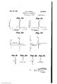
- Figures 2a to 2b inclusive are filter circuit characteristics, reac'tance characteristics, and
- Figures 4 and 5 illustrate the crystal filter characteristics when a low degree of off-neutralization is used.
- phase modulated energy from any source such as for example, a receiver of the heterodyne type, including an amplifier RFA and first detector and oscillator O, and intermediate frequency amplifier IFA may be impressed at any frequency such as for example intermediate frequency on the primary winding I2 of a transformer I0 having a secondary winding M connected at one terminal to a crystal 24 and the other terminal to neutralizing condensers I! and IS, the other terminals of which are connected to the crystal electrodes 26 and 25 respectively.
- the transformer II has its primary winding tuned and damped by a condenser l6 and resistance 2 while the secondary winding I4 is similarly tuned and damped by a condenser
- the midpoint of i4 is grounded as shown, thus completing a connection to the cathodes of tubes 28 and 30.
- the r n former 10 is tuned to subs ant al y themea frequency of the impressed wave energy and has a band pass characteristic.
- the electrode 25 of crystal 24 is connected to the control grid 34 of an electron discharge coupling and amplifying tube 29 by way of potentiometer 3
- the crystal 2d has its other electrode 2'3 connected to the control grid 36 of a second coupling and amplifying tube 3% through potentiometer 32.
- variable condensers fl and i9 feed neutralizing energy from the opposite end of the winding i l to electrodes 26 and 25 respectively.
- the capacity 19 between the input electrode 2'! and output electrode 25 is utilized to produce one filter effect and is adjusted to under-neutralize this circuit, i. e., produces the unneutralized filter effect.
- Condenser H is normally set so as to Over-neutralize the capacity of the crystal holder between the input electrode 27 and output electrode 26.
- crystal 24 has been connected in a circuit'which provides an unneutralized filter effect and an over-neutralized filter effect without the use of coupling tubes to produce this effect.
- the primary winding is tuned and properly damped by condenser 36 and resistance 33 respectively, while the secondary winding 42 is tuned by condenser 63 and damped by the diode input impedance.
- the anode of tube 39 is connected in a similar coupling and band pass transformer 35.
- the elements of this coupling circuit have been designated by numerals primed corresponding to the numerals used in describing the coupling transformer 35.
- Transformer 35 feeds the unneutralized energy to diode detector 50 while transformer 35 feeds over-neutralized energy to diode 52.
- the diode cathodes are connected together by resistors 48, 49.
- the detected output appears across the diode resistors 48, G9 and in this output variations in amplitude due to the phase modulations on the wave energy receiv'edaid while variations in amplitude due to undesired amplitude modulations on the received wave cancel in the output, as does the even harmonic distortion due to conversion of the phase modulation in the characteristic amplitude modulation.
- the output from 49, 48 may be sent to utilization circuit 60 and also to a frequency control circuit to accomplish automatic frequency control of the received wave.
- the energy present in transformer 35' is passed by 30 and 32 comprising a filter having an over-neutralized characteristic and having an input-output characteristic as shown in Figure 2e and having a reactance characteristic as shown in Figure 2]".
- the reactance of this last filter is positive or inductive on both sides of the carrier frequency except for a short interval near the carrier frequency. Consequently, the side bands are shifted 90 in phase by this filter also but in an opposite direction to the shift produced by filters having the characteristics shown in Figure 21).
- the phase modulated wave as shown in Figure 2g is converted to the amplitude modulated wave as shown in Figure 2h.
- Unwanted amplitude modulations on the wave received which is not converted to phase modulations by the action of the filters as described herein and in my United States Patent .#2,085,008 dated June 29, 1937, have the same or substantiallythe same effect on the energies passed by both filters and consequently due to the phase displaced combination of energies cancel each other more or less completely.
- the unwanted amplitude modulations which are converted to characteristic phase modulations have no effect on the diode detectors.
- the receiver described above is primarily adapted to the reception of phase modulation by converting phase modulation on the wave energy into corresponding modulations of opposing envelopes on wave energy portions which are then combined to reproduce the signals.
- circuits of this type for the reception of phase and amplitude modulated waves and also for the reception of waves modulated in amplitude or phase and to thereby eliminate the effect of fading on said waves which might change one type of modulation to the other andvice versa.
- the transformer 63 is coupled by a switch 65 toan output means 68 directly when 65 is in a left-hand position or by way of a frequency discriminating circuit 64 when the switch is in the right-hand position.
- the output of one single sideband detector is combined with the other with a phase difference in order to receive the modulation whether it comes in as phase or as amplitude modulation.
- the modulation as phase or amplitude modulation I do not intend to limit the modulation received to pure phase modulation or pure amplitude modulation, but have in mind modulation the characteristics of which resemble phase or amplitude modulation or varies between the two types of modulation. I have found'that with. a 90 phase displacement between the demodulated outputs of the single sidebands combining the outputs will reproduce the signal irrespective of changes in the character thereof between phase and amplitude modulation.
- and fil of Figure 3 are infiinite-im pedance diode detectors which are fed modulated energy passed by overand under-neutralized filter circuits.
- Tubes 62 and 62' are amplifier tubes the anodes of which may be connected in either push-pull or parallel depending upon the position of S1.
- the detected outputs of the infinite impedance diodes BI and 61 appear on "S and S".
- the cathode resistors and are pass'edto switches
- These switches may be ganged together so that when S is on point 1, S is also, and so on.
- the purpose of the switches is to connect in various values of blocking condensers which, in addition to the blocking of the diode direct current voltage from the grids of tubes 62 and 62', serve the following purposes: C1 is chosen with large enough Value so that it serves only the purpose of blocking and. in conjunction ll with the resistances R and R1 passes all frequencies with equal amplitude to the grids of tubes 62 and 62. With the switches on the point I phase modulation would be received with S1 adjusted for the push-pull connection.
- Condensers C2 are chosen small enough to reduce the amplitude of the lower modulating potentials so that their over-accentuation as an countered in amplitude modulation reception may be corrected. Hence, with S andS on point 2 and S1 thrown for push-push combination the adjustment is proper for amplitude modulation reception.
- switch S1 is set for the push-pull connection
- phase modulation is 90 and is obtained by the combined effect of condenser C0 and resistor R.
- the current through R will be determined mainly by the capacity C0 and the drop across the resistance will be shifted 90 from the voltage applied to point 0 on the switch.
- there is an attenuation such that the frequencies are passedin direct accordance with their frequency together with an attenuation of the average level.
- the reduction of the average level is compensated for by adjusting potentiometer R1 so that proper balance is'obtained between the energies amplified by tubes 62 and 62.
- the attenuation which causes the frequencies to be passed in direct accordance with their frequency produces an over-all output which rises as the frequency is increased.
- This rising characteristic may be compensated for by equalizer ti l 5' which is switched in by means of double-poledouble-throw switch 65.
- the equalizer fill may take the form of a tone control circuit such as is shown or may comprise any other of the known-forms of circuits for reducing the high frequencies with respect to the low frequencies.
- switch 65 When this phase-amplitude reception is adjusted for bysetting S and S on point El and throwing Si to either the push-pull or parallel condition, switch 65 would be thrown to the right to connect the equalizer in the circuit which feeds the output jack 66. For the other adjustments of either phase or amplitude modulation, switch 65 would be thrown to the left to disconnect 64 from the circuit.
- the tube El or El can be removed from the circuit or rendered inoperative by in-" terrupting its plate circuit when the switch is in position 1 and 2, depending on whether phase or amplitude modulation is being received. -This would make possible the reception of thecarrier and only one side band for the purpose of obtaining reception when the other side band happens to be interferedwith. For instance, ifthe true due to the fact that there can then be no cancellation effects between the upper and lower side bands since only one is being received. I
- Iclaim 1.
- a system for converting phase modulated wave energy to corresponding amplitude modulated wave energy an impedance, a piezo-electric crystal having three electrodes, a pair of output terminals connected by impedances a point on which is connected to a point on said first impedance, means for impressing wave energy to be converted on said first impedance, means coupling one of said crystalelectrodesto said first impedance, means coupling the other two of said crystal terminals each to one of said output electrodes, and reactive means coupling said one of said crystal electrodes to at least one of said pair of crystal electrodes to adjust the degree of neutralization of said crystal and, thereby adjust the characteristics of the filters formed by said crystal and connections.
- a wave receiver in combination anim pedance responsive to modulated wave energy, a pair of rectifiers each having input and output electrodes, a combining circuit, coupling means between said rectifier output electrodes and said combining circuit, phase shifting means in at least one of said coupling means, a pair of filters having characteristics such that each passes carrier energy and at least one sideband, a cou-- pling between the input of each filter and said impedance and a coupling between the outputs of said filters and the input electrodes of said rectifiers.
- a pair of rectifiers each having input and output electrodes, 2. combining circuit, coupling means between said rectifier output electrodes and said combining circuit, phase shifting means in at least one of said coupling means, a pair ofcrystal filters comprising a piezoelectric crystal and a plurality of crystal electrodes associated therewith, each filter having a characteristic such that it passes the carrier and a sideband, a coupling between the inputs of said filters and said impedance, and a coupling between the output of each filter and the input electrodes of adifierent one of said rectifiers.
- a wave receiver in combination, an impedance responsive to modulated wave energy, a pair of rectifiers each having input and output electrodes, a combining circuit, coupling means between said rectifier outputs and said combining circuit, phase shifting means in at least one of said coupling means, a pair of filter circuits comprising in combination a piezo-electric crystal having a plurality of electrodes, one of which serves as aninput and is coupled to said impedance, another pair of which electrodes serve as outputs coupled to the input electrodes of said rectifiers, and means for adjusting the reoutput electrodes, phase shifting means in at least one of said coupling means, a pair of filter circuits comprising a piezo-electric crystal having a plurality of electrodes, one of which is coupled to said impedance and a pair of which is coupled to output'terminals, a pair of coupling tubes having input and output electrodes, means connecting the input electrodes of said coupling tubes to said output terminals, means coupling the output electrodes of said coupling tubes to the
- a wave receiver in combination, an impedance responsive to modulated wave energy, a pair of rectifiers each having input and output electrodes, a combining circuit, a utilization circuit, a modulation potential frequency discriminating circuit, switching means for coupling said utilization circuit directly to said combining circuit or through said frequency discrimihating circuit to said combining circuit, coupling means between said rectifier output electrodes and said combining circuit, phase shifting means in at least one of said coupling means, a pair of filters having characteristics such that each passes the carrier and a difierent sideband, said filters having inputs and outputs, a coupling betweentthe input of each filter and said impedance and a coupling between the output of each filter and the input electrodes of a difierent one of said rectifiers.
- a wave responsive receiver in combination, an impedance responsive to modulated wave energy, a pair of rectifiers each having input and output electrodes, a combining circuit, networks each comprising series capacity and shunt resistance connecting the output electrodes of said rectifiers to said combining circuit, saidresistive networks serving to relatively shift the phase of the energies passed thereby from said rectifier output, electrodes to said combining circuit, a pair of filters having characteristics such that each passes the carrier and a different sideband, a coupling between the input of each filter and said impedance and couplings between the outputs of said filters and the input electrodes of said rectifiers.
- a system for filtering modulated wave energy an impedance, a utilization circuit, a plurality of coupling tubes having input electrodes and having output electrodes coupled to said utilization circuit, means for impressing modulated wave energy on said impedance, a piezoelectric crystal having a pluralityvof electrodes, means coupling one of said electrodes to said impedance, means coupling other ofsaid crystal electrodes to the input electrodes of said coupling tubes, means for varying the degree of neutralization of the reactance between pairs of said crystal electrodes and means for relatively adjusting the gain characteristics of saidcoua pling tubes.
- a wave receiver in combination, an impedance responsive to modulated wave energy, a pair of rectifiers each having input and output electrodes, a combining circuit, couplingmeans between said rectifier output electrodes and said combining circuit, a filter having characteristic such that it exalts the carrier and attenuates one sideband, a second filter having a portion in common with said first filter and having a characteristic such that it exalts the carrier and attenuates the other side-band, said filters having inputs and outputs, a coupling between the input of said filters and said impedance and couplings between the outputs of said filters and the rectifier inputs.
- a wave receiver in combination, an impedance responsive tomodulated wave energy, a pair of rectifiers each having input and output electrodes, switching means connected with said rectifier output electrodes for combining the outputs thereof in phase or in phase opposition, a pair of filters each having characteristics such that each eXalts the carrier and passes the sidebands with different amounts of attenuation, a coupling between the inputs of said filters and said impedance and a coupling between the outputs of said filters and a diiferent one, of said rectifier input electrodes,
- a reactance tuned to substantially the mean frequency of the wave energy
- a pair of electron discharge rectifier tubes each having input and output electrodes
- a piezo-electric crystal having an input electrode and a pair of output electrodes, a connection between said input electrode and said tuned reactance, a coupling between each of the output electrodes of said crystal and the input electrodes in a different one of said rectifier tubes, and variable reactances coupling said first reactance to each of said output electrodes of said crystal to adjust the degree of neutralizationof sai crystal electrodes.
- a reactance tuned to substantially the mean frequency of the wave energy
- a pair of electron discharge coupling tubes each having a controlling electrode, a cathode, and an anode
- a rectifier system circuits tuned to substantially the mean frequency of said wave energy coupling the anode and cathode of each of said coupling tubes to said rectifier system
- a piezo-electric crystal having an input electrode and a pair of output electrodes, a connection between said input electrode and said tuned reactance, a connection between the cathodes of said coupling tubes and said tuned reactance, a connection between each of the output electrodes of said crystal and a controlling electrode in a different one vof said coupling tubes, and a variable reactance coupling said first reactance to each of said output electrodes of said crystal.
- a system for demodulating modulated wave energy the signal'modulations on which may, due to fading or other causes, have characteristics of phase or amplitude modulation or both
- means for amplifying said modulated wave energy means excited by the amplified wave energy for producing two oscillating voltages the amplitudes of which substantially correspond to the modulations on the said wave energy irrespective of the characteristics of the modulation on said wave energy, means for demodulating said oscillating voltages, and means for com,- bining'the demodulated components in substantially 90 phase relation to produce a resultant representing the signal.
- means for modifying the potentials of the said resultant in accordance with the frequency thereof has an input coupled to said combining means and an output from which the modified potentials may be derived.
- separate means for separately amplifying each side band and said carrier wave separate rectifying means each having an input coupled to a different one of said amplifying means, said rectifying means each having an output, means for combining the outputs from said rectifiers said combining means having an input coupled to the output of each of said rectifying means, and phase shifting means in one of said couplings.
- means for modifying the resultant of the energies in said combining means in accordance with their frequency has an input coupled to said combining means and an output from which resulting modified potentials may be derived.
Landscapes
- Engineering & Computer Science (AREA)
- Power Engineering (AREA)
- Oscillators With Electromechanical Resonators (AREA)
- Digital Transmission Methods That Use Modulated Carrier Waves (AREA)
Description
3 Sheets-Sheet 1 CROSBY June 18,
PHASE MODULATION RECEIVER Filed March 10, 1938 .zmuno win/:1
INVENTOR. MURRAY 6. CROSBY Irvin-pa 111-1111 ATTORNEY.
June 18, 1940. G, mossy PHASE MODULATION RECEIVER Filed March 10, 1938 3 Sheets-Sheet I5 vvvv vf F AMPLIFIER GAIN CONTROLLED R F AMPLIFIER AND la osrscrok E I I 1"" MuRkfl l kY ATTORNEY.
Patented June 18, 1940 PATENT 2,204,575 PHASE MODULATION RECEIVER Murray G. Crosby, Riverhead, N. Y., assignor to Radio Corporation of America, a corporation of Delaware Application March 10, 1938, Serial No. 195,041
17 Claims.
In my United States Patent #2,085,008 dated June 29, 1937, I have disclosed means for demodulating phase modulated energy which includes a filter circuit having therein a crystal the capacity of the holder of which is unneutralized so that the filter, if substantially resonant at the mean frequency of the wave energy to be demodulated, is reactive in the same sense on both sides of the said mean or carrier frequency. Thus,
when the phase modulated wave energy is passed through this crystal filter circuit, the sidebands are rotated 90 in the same direction relative to the carrier. To one skilled in the art it will be apparent that this crystal filter, including the crystal with the unneutralized holder, will convert phase modulated wave energy passed thereby, to characteristic amplitude modulated wave energy because rotating the sidebands in the same direction 90 is the same as shifting the carrier with respect to the sidebands 90 resulting in a carrier and sideband relation as in amplitude modulation.
In my United States application #165,056 filed September 22, 1937, now Patent #2,156,374 issued May 2, 1939, I have utilized the principle or fundamental feature disclosed in Patent #2,085,008 dated June 29, 1937, in a novel manner to obtain the advantage to, be gained by back-t'o-back reception. In this latter application I utilize a single crystal in an under-neutralized circuit and the same crystal in an over-neutralized circuit with the circuit outputs connected by coupling tubes to diode rectifiers in such a manner that the envelopes of the amplitude modulations resulting from the conversion of the phase modulated wave as described in connection with Patent #2,085,008 dated June 29, 1937, are 180 out of phase. As'a consequence, in the combined output of the detectors the converted amplitude b modulations aid or add to produce a resultant characteristic of the phase modulations on the waves, while any undesired amplitude modulations on the wave which produce corresponding effects in the two filter effects oppose and sub- 5 stantially cancel. This 180 phase relation of the envelopes of the amplitude modulations re-, sulting from conversion is obtained because an under-neutralized and an over-neutralized filter converts the phase modulations to characteristic 50 amplitude modulations of opposed polarity. These two amplitude modulations are detected and combined in push-pull so that the phase modulations aid, that is, the characteristic am plitude modulations resulting from the phase to modulations on the Waves aid while the amplitude modulations present on the original unconverted wave oppose. The even harmonic distortion of the phase modulation is also balanced out by the back-to-iback type of detection.
In my United States application #167,344 filed October 5, 1937, now Patent #2,156,375 issued May 2, 1939, I disclose a receiver of the type described in my United States application #165,056 filed September 22, 1937, now Patent #2,156,374 issued May 2, 1939. However, in the 10 receiver disclosed in application #167,344 filed October 5, 1937, now Patent #2,156,375 issued May 2, 1939, I utilize two crystals, one of which is under-neutralized and the other of which is over-neutralized. The outputs of these crystals 15 are converted characteristic amplitude modulated wave energy having envelopes of opposed polarity and are added as in the circuit of application #165,056 filed September 22, 1937, now Patent #2,156,374 issued May 2, 1939. The use of two 20 crystals simplifies the circuit arrangements in some respects and in a modification permits elimination of the coupling tubes used in the other modifications for overor under-neutralizing the crystal holder capacity. 5
In the present disclosure which utilizes the principles of operation disclosed in the second and third applications referred to above, an improved receiver or converting circuit is shown in which a back-to-back receiver effect is obtained '30 by means of converting circuits whichutilize a single crystal in a three-electrode holder connected with a push-pull circuit excited by the wave energy to be converted and to demodulators for demodulating the converted energy. Here, 35 as in the prior applications, two filters are arranged and connected in over-neutralized and under-neutralized circuits respectively, with the outputs so connected with the detectors that phase modulations on the original wave result 4 in corYesponding amplitude modulations, the envelopes of which are opposed, resulting in addition of the characteristic amplitude modulations caused by the phase modulations on the wave energy and bucking and cancelling of changes in the converted energy due to undesired amplitude modulation on the received wave energy. By the use of three-electrode crystal holders, two filtered outputs are available from a single crystal. One filter has an over-neutralized characteristic while the other filter has an underneutralized characteristic. Neutralizing and over-neutralizing in the present case is accomplished without the use of coupling tubes as in I8 and and resistance 20.
ber 22, 1937, now Patent #2,156,3'74 issued May 2, 1939. The use of a single crystal is advantageous because'of the dil'ficuity in grinding a plurality of crystals to the same frequency. Since it is not necessary to neutralize through coupling tubes the circuit is simplified.
The present application concerns also a new and improved method of and means for adapting the novel receiver described above to the reception of wave energy the characteristic of which may resemble most amplitude or phase modu- .q
lated energy or may vary between amplitude and phase modulation due to fading or other causes. In accomplishing this the crystal filters are slightly off-neutralized to get single sideband effects. The detected output due to one sideband is shifted in phase about and the energies combined. The 90 phase displacement is desired because I have found that fading distorts the wave from phase to amplitude modulation and vice versa. I have found that if the outputs of the demodulated sidebands are combined in phase any phase modulations on the wave cancel and the amplitude modulations 0n the Wave are reproduced. I have also found that if the outputs of the demodulated sidebands are combined in opposition the phase modulations on the wave are reproduced while the amplitude modulations oppose and cancel. Hence, I propose to introduce in the outputs resulting from demodulation of .the sidebands, a relative phase displacement of about 90 so that phase and amplitude modulations on the wave are reproduced in the combined outputs. Thus, if the modulations on the wave are changed during transmission or from phase to amplitude or vice versa still the modulations are reproduced by combining the outputs.
Describing my invention in detail, reference will be made to the attached drawings wherein:
Figures 1 and 3 each show filter circuits including a piezo-electric crystal in a three-electrode holder connected in two filter circuits for converting phase modulated wave energy to a characteristic amplitude modulated wave energy and demodulating the same. In Figure l a high degree of off-neutralizedcrystal effect is utilized. In Figure 3 a high or low degree of ofi-neutralized effect is utilized;
Figures 2a to 2b inclusive, are filter circuit characteristics, reac'tance characteristics, and
modulated wave energy vector diagrams used in describing the operation of my receiver;
Figures 4 and 5 illustrate the crystal filter characteristics when a low degree of off-neutralization is used.
Referring to Figure 1 phase modulated energy from any source such as for example, a receiver of the heterodyne type, including an amplifier RFA and first detector and oscillator O, and intermediate frequency amplifier IFA may be impressed at any frequency such as for example intermediate frequency on the primary winding I2 of a transformer I0 having a secondary winding M connected at one terminal to a crystal 24 and the other terminal to neutralizing condensers I! and IS, the other terminals of which are connected to the crystal electrodes 26 and 25 respectively. The transformer II) has its primary winding tuned and damped by a condenser l6 and resistance 2 while the secondary winding I4 is similarly tuned and damped by a condenser The midpoint of i4 is grounded as shown, thus completing a connection to the cathodes of tubes 28 and 30. The r n former 10 is tuned to subs ant al y themea frequency of the impressed wave energy and has a band pass characteristic. The electrode 25 of crystal 24 is connected to the control grid 34 of an electron discharge coupling and amplifying tube 29 by way of potentiometer 3|. The crystal 2d has its other electrode 2'3 connected to the control grid 36 of a second coupling and amplifying tube 3% through potentiometer 32. The variable condensers fl and i9 feed neutralizing energy from the opposite end of the winding i l to electrodes 26 and 25 respectively. The capacity 19 between the input electrode 2'! and output electrode 25 is utilized to produce one filter effect and is adjusted to under-neutralize this circuit, i. e., produces the unneutralized filter effect. Condenser H is normally set so as to Over-neutralize the capacity of the crystal holder between the input electrode 27 and output electrode 26. Thus, crystal 24 has been connected in a circuit'which provides an unneutralized filter effect and an over-neutralized filter effect without the use of coupling tubes to produce this effect. Moreover, I have found that this overneutralizing from the output of one electrode, say 26, does not in any way impair the characteristic of .the other electrode, say 25, which is underneutralized, so that the characteristic fed to coupling and amplifying tube 29 is that of an unneutralized filter and the characteristic fed to the coupling tube 30 is that of an over-neutralized filter. Potentiometers 3i and 32 furnish a direct current return for the grids 34 and 36 of the coupling tubes, while resistor 33 properly bypassed, furnishes self-bias for the tubes. The anode of tube 29 is connected to the primary winding fll of a coupling band pass transformer 35 having a secondary Winding 42. The primary winding is tuned and properly damped by condenser 36 and resistance 33 respectively, while the secondary winding 42 is tuned by condenser 63 and damped by the diode input impedance. The anode of tube 39 is connected in a similar coupling and band pass transformer 35. The elements of this coupling circuit have been designated by numerals primed corresponding to the numerals used in describing the coupling transformer 35. Transformer 35 feeds the unneutralized energy to diode detector 50 while transformer 35 feeds over-neutralized energy to diode 52. The diode cathodes are connected together by resistors 48, 49. As shown, the detected output appears across the diode resistors 48, G9 and in this output variations in amplitude due to the phase modulations on the wave energy receiv'edaid while variations in amplitude due to undesired amplitude modulations on the received wave cancel in the output, as does the even harmonic distortion due to conversion of the phase modulation in the characteristic amplitude modulation. The output from 49, 48 may be sent to utilization circuit 60 and also to a frequency control circuit to accomplish automatic frequency control of the received wave.
In the operation of the receiver of Figure 1 two filter characteristics are produced to be fed to the two diode detectors 50 and 52. The energy fed from the crystal output terminal 25 to ampli' fier and coupling tube 29 is unneutralized crystal energy and has a characteristic as shown in Figure 2a. This energy appears in transformer 35. The characteristic of the energy present in transformer 35 is as shown in Figure 26 being derived from a filter of the overneutralized type such as is obtained by over-neutralizing the hol rele trqdes 26 an 3W me of 'l- This 15 24. These. two. crystal filter characteristics as shown in Figures 2a and 2e have reactance char-. acteristics as shown in Figures 2b and 2 respectively. In the case of Figure 2b a. negative reactance is present on both sides of the carrier frequency, that is, the circuit would be capacitive resistive at the carrier frequency, the phase of the side bands will be shifted 90 with respect to the carrier. In Figure 2c the carrier and side bands of a phase modulated wave are shown. The carrier is marked C, the upper side band U, and the lower side band L. The positive direction of rotation is taken, as clockwise and the directions of rotation of the side bands with respect to the carrier are indicated by arrows attached to the side band vectors. Side bands of an order greater than 1 have been neglected due to their small amplitude andfor simplicity of explanation. When the phase modulated wave of Figure 2c is passed through the crystal having the characteristic of Figure 2a and the reactance characteristic of Figure2b the side bands are shifted 90 with respect to the carrier so that the side band relation shown in Figure 2d is effected. As is known to the art, with the relation as shown in Figure 2d between the carrier and. side bands, the wave is an amplitude modulated wave. There would also be an attenuation of the side bands which is not shown in Figure 2d. This conversion of the phase modulated wave as of 20. to an amplitude modulated wave as of 2d takes place in 21, 24, 25, and 29, and the converted energy appears in 35.
The energy present in transformer 35' is passed by 30 and 32 comprising a filter having an over-neutralized characteristic and having an input-output characteristic as shown in Figure 2e and having a reactance characteristic as shown in Figure 2]". Thus, the reactance of this last filter is positive or inductive on both sides of the carrier frequency except for a short interval near the carrier frequency. Consequently, the side bands are shifted 90 in phase by this filter also but in an opposite direction to the shift produced by filters having the characteristics shown in Figure 21). Hence the phase modulated wave as shown in Figure 2g is converted to the amplitude modulated wave as shown in Figure 2h. From an examination of Figure 2d and Figure 2h it can be seen that the side bands are appreaching cancellation of the carrier in Figure 2d and are approaching aiding the carrier in Figure 271.. Thus, the envelope of the amplitude modulations produced by the two filters having characteristics as shown above are 180 apart and their detected output must be combined in a push-pull or series combination to reproduce the converted modulations instead of a parallel combination. This combination is effected in the diode circuit of Figure l by reversing the connections of one of the diode resistors 48 and 49 as shown and connecting the same-in series to produce the receiver output. Unwanted amplitude modulations on the wave received, which is not converted to phase modulations by the action of the filters as described herein and in my United States Patent .#2,085,008 dated June 29, 1937, have the same or substantiallythe same effect on the energies passed by both filters and consequently due to the phase displaced combination of energies cancel each other more or less completely. The unwanted amplitude modulations which are converted to characteristic phase modulations have no effect on the diode detectors.
By an examination of the filter characteristics of Figures 2a and 2e it can be seen that when the carrier frequency drifts the relative amplitudes of the two filter outputs vary differentially. That is, as the frequency drifts lower the output of the filter of Figure 2e approaches the dip point whereas the output of the filter of Figure 2a reduces more gradually. This results in adiiferential action which produces differential detected energy which may be used for automatic frequency control purposes. This differential potential may act through a time constant circuit TC on a reactance tube M the reactance of i 53 and 53' along a potentiometer resistances R and R. Proper adjustment of the under-neutralizing and over-neutralizing condensers l'l and IQ of Figure 3 is required tobalance the filter characteristics with respect to the shapes of the characteristics. In addition, balance may be obtained by adjusting the arms on the potentiometers 3|, 32 so as to allow the stronger output to be reduced to the weaker.
The receiver described above is primarily adapted to the reception of phase modulation by converting phase modulation on the wave energy into corresponding modulations of opposing envelopes on wave energy portions which are then combined to reproduce the signals. In many cases it is desirable to use circuits of this type for the reception of phase and amplitude modulated waves and also for the reception of waves modulated in amplitude or phase and to thereby eliminate the effect of fading on said waves which might change one type of modulation to the other andvice versa. I have provided, as will now be described in connection with Figure 3, a method of and means for accomplishing the above objects, it being noted that in accomplishing the said objects I have also provided a diversity eifect in that my novel method and means uses both side bands of phase or amplitude modulated waves which duehto fading or other cause have been changed to simulate amplitude and phase modulated waves respectively.
The receiver in Figure 3 up to the diode detectors 50 and 52 is substantially the same as the receiver of Figure 1- and this portion of the receiver will not be described in detail herein. In the prior operation of these receivers, as has been pointed out, the crystal filters including 21 and 25 and 21 and 26 have been adjusted for a considerable overand under-neutralization as indicated by Figures 2a to 2h inclusive. As pointed out in my United States application #186,273 filed January 22, 19-38, I find that by adjusting the crystal filters so that one has a very small amount of negative reactance across its holder and the other of very small positive reactance, a single sideband effect is obtained as shown in Figures 4 and 5. 1 This "effect is obtained here by underand over-neutralizing the crystals relatively small amounts. With the crystal holder neutralized in this way the output on the side of the carrier frequency which does not'have the rejection point, is higher than the output or other side having the rejection point, consequently one of the filters exhalts thecarrier and selects the lower si-deband while the other filter exhalts the carrier and selects the upper sideband. I make use of this principle in the present invention to obtain single sideband effects as described in my United States application #565,005 filed September 29, 1931, Patent #1114335, patented April 19, 1938, to adapt this receiver to the receptionof phase or amplitude modulated waves and to the reception of waves which, due to any causes whatever, vary in characteristics so that they change from phase to amplitude and vice versa during reception. This sideband effect is necessary in order to use balanced detectors with the audio outputs combined in push-pull where it is to be used for phase modulation only and push-push where the receiver is to be used for amplitude modulation only. The differential connection of the detectors-is also necessary to obtain automatic frequency control potentials. Referring more specifically to Figure 3 the outputs of 50 and 52 are combined differentially of a necessity in order to supply to M the desired potentials necessary for frequency control purposes. The outputs of secondaries 42 and 42 are also supplied'as shown to controlling electrodes 5'! and 59 of infinite impedance diode detector tubes GI and iii. The cathodes of tubes El and 6! are connected as shown by way of switching circuits described more in detail hereinafter to the controlling electrodes 61, 68 of combining tubes 62, 62, the anodes of which are connected with a transformer 63 by way of switch S1, which permits the outputs of 62 and 62 to be aided in push-pull relation where phase modulated wave energy is to be received or in parallel when amplitude modulated wave energy is to be received. The transformer 63 is coupled by a switch 65 toan output means 68 directly when 65 is in a left-hand position or by way of a frequency discriminating circuit 64 when the switch is in the right-hand position.
As stated above, in this system the output of one single sideband detector, say for example the output of BI, is combined with the other with a phase difference in order to receive the modulation whether it comes in as phase or as amplitude modulation. In referring to the modulation as phase or amplitude modulation I do not intend to limit the modulation received to pure phase modulation or pure amplitude modulation, but have in mind modulation the characteristics of which resemble phase or amplitude modulation or varies between the two types of modulation. I have found'that with. a 90 phase displacement between the demodulated outputs of the single sidebands combining the outputs will reproduce the signal irrespective of changes in the character thereof between phase and amplitude modulation.
Tubes 6| and fil of Figure 3 are infiinite-im pedance diode detectors which are fed modulated energy passed by overand under-neutralized filter circuits. Tubes 62 and 62' are amplifier tubes the anodes of which may be connected in either push-pull or parallel depending upon the position of S1. The detected outputs of the infinite impedance diodes BI and 61 appear on "S and S".
. for the combination of the separately detected the cathode resistors: and are pass'edto switches These switches may be ganged together so that when S is on point 1, S is also, and so on. The purpose of the switches is to connect in various values of blocking condensers which, in addition to the blocking of the diode direct current voltage from the grids of tubes 62 and 62', serve the following purposes: C1 is chosen with large enough Value so that it serves only the purpose of blocking and. in conjunction ll with the resistances R and R1 passes all frequencies with equal amplitude to the grids of tubes 62 and 62. With the switches on the point I phase modulation would be received with S1 adjusted for the push-pull connection.
Condensers C2 are chosen small enough to reduce the amplitude of the lower modulating potentials so that their over-accentuation as an countered in amplitude modulation reception may be corrected. Hence, with S andS on point 2 and S1 thrown for push-push combination the adjustment is proper for amplitude modulation reception. I
The remaining point 0 for switches S and S is switch S1 is set for the push-pull connection,
only phase modulation will be received and if it is set'for the push-push connection only am plitude modulation will be received. Consequently, in order to receive both types, a phase of combination must be chosen such that there will be no bucking effect between the two halves of the balanced detectors. bination is 90 and is obtained by the combined effect of condenser C0 and resistor R. By making Co of high reactance compared to R, the current through R will be determined mainly by the capacity C0 and the drop across the resistance will be shifted 90 from the voltage applied to point 0 on the switch. Concomitant with the phase shift introduced by the combination COR, there is an attenuation such that the frequencies are passedin direct accordance with their frequency together with an attenuation of the average level. The reduction of the average level is compensated for by adjusting potentiometer R1 so that proper balance is'obtained between the energies amplified by tubes 62 and 62. The attenuation which causes the frequencies to be passed in direct accordance with their frequency produces an over-all output which rises as the frequency is increased. This rising characteristic may be compensated for by equalizer ti l 5' which is switched in by means of double-poledouble-throw switch 65. The equalizer fill may take the form of a tone control circuit such as is shown or may comprise any other of the known-forms of circuits for reducing the high frequencies with respect to the low frequencies. When this phase-amplitude reception is adjusted for bysetting S and S on point El and throwing Si to either the push-pull or parallel condition, switch 65 would be thrown to the right to connect the equalizer in the circuit which feeds the output jack 66. For the other adjustments of either phase or amplitude modulation, switch 65 would be thrown to the left to disconnect 64 from the circuit.
Hence, in order to This phase of com- 4! If desired the tube El or El can be removed from the circuit or rendered inoperative by in-" terrupting its plate circuit when the switch is in position 1 and 2, depending on whether phase or amplitude modulation is being received. -This would make possible the reception of thecarrier and only one side band for the purpose of obtaining reception when the other side band happens to be interferedwith. For instance, ifthe true due to the fact that there can then be no cancellation effects between the upper and lower side bands since only one is being received. I
Iclaim: 1. In a system for converting phase modulated wave energy to corresponding amplitude modulated wave energy, an impedance, a piezo-electric crystal having three electrodes, a pair of output terminals connected by impedances a point on which is connected to a point on said first impedance, means for impressing wave energy to be converted on said first impedance, means coupling one of said crystalelectrodesto said first impedance, means coupling the other two of said crystal terminals each to one of said output electrodes, and reactive means coupling said one of said crystal electrodes to at least one of said pair of crystal electrodes to adjust the degree of neutralization of said crystal and, thereby adjust the characteristics of the filters formed by said crystal and connections. I
2. In a wave receiver in combination anim pedance responsive to modulated wave energy, a pair of rectifiers each having input and output electrodes, a combining circuit, coupling means between said rectifier output electrodes and said combining circuit, phase shifting means in at least one of said coupling means, a pair of filters having characteristics such that each passes carrier energy and at least one sideband, a cou-- pling between the input of each filter and said impedance and a coupling between the outputs of said filters and the input electrodes of said rectifiers.
3. In a wave receiver in combination, an impedance responsive to modulated Wave energy,
a pair of rectifiers each having input and output electrodes, 2. combining circuit, coupling means between said rectifier output electrodes and said combining circuit, phase shifting means in at least one of said coupling means, a pair ofcrystal filters comprising a piezoelectric crystal and a plurality of crystal electrodes associated therewith, each filter having a characteristic such that it passes the carrier and a sideband, a coupling between the inputs of said filters and said impedance, and a coupling between the output of each filter and the input electrodes of adifierent one of said rectifiers.
4. In a wave receiver in combination, an impedance responsive to modulated wave energy, a pair of rectifiers each having input and output electrodes, a combining circuit, coupling means between said rectifier outputs and said combining circuit, phase shifting means in at least one of said coupling means, a pair of filter circuits comprising in combination a piezo-electric crystal having a plurality of electrodes, one of which serves as aninput and is coupled to said impedance, another pair of which electrodes serve as outputs coupled to the input electrodes of said rectifiers, and means for adjusting the reoutput electrodes, phase shifting means in at least one of said coupling means, a pair of filter circuits comprising a piezo-electric crystal having a plurality of electrodes, one of which is coupled to said impedance and a pair of which is coupled to output'terminals, a pair of coupling tubes having input and output electrodes, means connecting the input electrodes of said coupling tubes to said output terminals, means coupling the output electrodes of said coupling tubes to the input electrodes of said rectifiers, and means for adjusting the reactance between pairs of said crystal electrodes to thereby adjust the characteristics of said filter circuits so that each passes carrier energy and a different sideband. I
6. In a wave receiver in combination, an impedance responsive to modulated wave energy, a pair of rectifiers each having input and output electrodes, a combining circuit, a utilization circuit, a modulation potential frequency discriminating circuit, switching means for coupling said utilization circuit directly to said combining circuit or through said frequency discrimihating circuit to said combining circuit, coupling means between said rectifier output electrodes and said combining circuit, phase shifting means in at least one of said coupling means, a pair of filters having characteristics such that each passes the carrier and a difierent sideband, said filters having inputs and outputs, a coupling betweentthe input of each filter and said impedance and a coupling between the output of each filter and the input electrodes of a difierent one of said rectifiers. 1
7. In a wave responsive receiver in combination, an impedance responsive to modulated wave energy, a pair of rectifiers each having input and output electrodes, a combining circuit, networks each comprising series capacity and shunt resistance connecting the output electrodes of said rectifiers to said combining circuit, saidresistive networks serving to relatively shift the phase of the energies passed thereby from said rectifier output, electrodes to said combining circuit, a pair of filters having characteristics such that each passes the carrier and a different sideband, a coupling between the input of each filter and said impedance and couplings between the outputs of said filters and the input electrodes of said rectifiers.
8. In a system for filtering modulated wave energy, an impedance, a utilization circuit, a plurality of coupling tubes having input electrodes and having output electrodes coupled to said utilization circuit, means for impressing modulated wave energy on said impedance, a piezoelectric crystal having a pluralityvof electrodes, means coupling one of said electrodes to said impedance, means coupling other ofsaid crystal electrodes to the input electrodes of said coupling tubes, means for varying the degree of neutralization of the reactance between pairs of said crystal electrodes and means for relatively adjusting the gain characteristics of saidcoua pling tubes.
9. In a system for filtering modulated wave energy, an impedance, a plurality of coupling tubes each having input electrodes and output electrodes, and a screening electrode between put electrodes of said coupling tubes, means shunting the electrodes of said crystal for varying the degree of neutralization of the reactance between pairs of said crystal electrodes, and means for impressing adjustable potentials on said screening electrodes to thereby control the gain of said coupling tubes.
10. In a wave receiver in combination, an impedance responsive to modulated wave energy, a pair of rectifiers each having input and output electrodes, a combining circuit, couplingmeans between said rectifier output electrodes and said combining circuit, a filter having characteristic such that it exalts the carrier and attenuates one sideband, a second filter having a portion in common with said first filter and having a characteristic such that it exalts the carrier and attenuates the other side-band, said filters having inputs and outputs, a coupling between the input of said filters and said impedance and couplings between the outputs of said filters and the rectifier inputs.
11. In a wave receiver in combination, an impedance responsive tomodulated wave energy, a pair of rectifiers each having input and output electrodes, switching means connected with said rectifier output electrodes for combining the outputs thereof in phase or in phase opposition, a pair of filters each having characteristics such that each eXalts the carrier and passes the sidebands with different amounts of attenuation, a coupling between the inputs of said filters and said impedance and a coupling between the outputs of said filters and a diiferent one, of said rectifier input electrodes,
12. In a system for converting phase modulated wave energy to corresponding amplitude modulated wave energy and substantially eliminating from said converted energy any variations due to amplitude modulations on the wave energy, a reactance tuned to substantially the mean frequency of the wave energy, a pair of electron discharge rectifier tubes each having input and output electrodes, a piezo-electric crystal having an input electrode and a pair of output electrodes, a connection between said input electrode and said tuned reactance, a coupling between each of the output electrodes of said crystal and the input electrodes in a different one of said rectifier tubes, and variable reactances coupling said first reactance to each of said output electrodes of said crystal to adjust the degree of neutralizationof sai crystal electrodes.
' 13. In' a system for converting phase modulated wave energy to corresponding amplitude modulated wave energy and substantially eliminating from said converted energy any variations due to amplitude modulations on the wave energy, a reactance tuned to substantially the mean frequency of the wave energy, a pair of electron discharge coupling tubes each having a controlling electrode, a cathode, and an anode, a rectifier system, circuits tuned to substantially the mean frequency of said wave energy coupling the anode and cathode of each of said coupling tubes to said rectifier system, a piezo-electric crystal having an input electrode and a pair of output electrodes, a connection between said input electrode and said tuned reactance, a connection between the cathodes of said coupling tubes and said tuned reactance, a connection between each of the output electrodes of said crystal and a controlling electrode in a different one vof said coupling tubes, and a variable reactance coupling said first reactance to each of said output electrodes of said crystal.
14. In a system for demodulating modulated wave energy the signal'modulations on which may, due to fading or other causes, have characteristics of phase or amplitude modulation or both, means for amplifying said modulated wave energy, means excited by the amplified wave energy for producing two oscillating voltages the amplitudes of which substantially correspond to the modulations on the said wave energy irrespective of the characteristics of the modulation on said wave energy, means for demodulating said oscillating voltages, and means for com,- bining'the demodulated components in substantially 90 phase relation to produce a resultant representing the signal.
15.A system as recited in claim 14 wherein means for modifying the potentials of the said resultant in accordance with the frequency thereof has an input coupled to said combining means and an output from which the modified potentials may be derived.
16. In a system for demodulating modulated wave energy comprising a carrier and side bands the characteristics of which wave energy may indicate phase or amplitude modulation or both,
, separate means for separately amplifying each side band and said carrier wave, separate rectifying means each having an input coupled to a different one of said amplifying means, said rectifying means each having an output, means for combining the outputs from said rectifiers said combining means having an input coupled to the output of each of said rectifying means, and phase shifting means in one of said couplings.
17. A system as recited in claim 16 wherein means for modifying the resultant of the energies in said combining means in accordance with their frequency has an input coupled to said combining means and an output from which resulting modified potentials may be derived.
MURRAY G. CROSBY.
Priority Applications (2)
| Application Number | Priority Date | Filing Date | Title |
|---|---|---|---|
| US195041A US2204575A (en) | 1938-03-10 | 1938-03-10 | Phase modulation receiver |
| GB7873/39A GB526259A (en) | 1938-03-10 | 1939-03-10 | Improvements in or relating to modulated carrier wave receivers |
Applications Claiming Priority (1)
| Application Number | Priority Date | Filing Date | Title |
|---|---|---|---|
| US195041A US2204575A (en) | 1938-03-10 | 1938-03-10 | Phase modulation receiver |
Publications (1)
| Publication Number | Publication Date |
|---|---|
| US2204575A true US2204575A (en) | 1940-06-18 |
Family
ID=22719845
Family Applications (1)
| Application Number | Title | Priority Date | Filing Date |
|---|---|---|---|
| US195041A Expired - Lifetime US2204575A (en) | 1938-03-10 | 1938-03-10 | Phase modulation receiver |
Country Status (2)
| Country | Link |
|---|---|
| US (1) | US2204575A (en) |
| GB (1) | GB526259A (en) |
Cited By (2)
| Publication number | Priority date | Publication date | Assignee | Title |
|---|---|---|---|---|
| US2984791A (en) * | 1959-01-15 | 1961-05-16 | Frequency modulation reception circuits | |
| US3158817A (en) * | 1961-08-30 | 1964-11-24 | Donald M Lauderdale | Frequency responsive apparatus with dual output filter |
-
1938
- 1938-03-10 US US195041A patent/US2204575A/en not_active Expired - Lifetime
-
1939
- 1939-03-10 GB GB7873/39A patent/GB526259A/en not_active Expired
Cited By (2)
| Publication number | Priority date | Publication date | Assignee | Title |
|---|---|---|---|---|
| US2984791A (en) * | 1959-01-15 | 1961-05-16 | Frequency modulation reception circuits | |
| US3158817A (en) * | 1961-08-30 | 1964-11-24 | Donald M Lauderdale | Frequency responsive apparatus with dual output filter |
Also Published As
| Publication number | Publication date |
|---|---|
| GB526259A (en) | 1940-09-13 |
Similar Documents
| Publication | Publication Date | Title |
|---|---|---|
| US2065565A (en) | Automatic frequency control system | |
| US2243417A (en) | Frequency modulation receiver | |
| US2410983A (en) | Discriminator-rectifier circuit | |
| US2561088A (en) | Combined amplitude and frequency modulation detectors | |
| US2044745A (en) | Receiving circuits | |
| US2425922A (en) | Frequency discriminator circuit | |
| US2519890A (en) | Angle modulated wave receiver | |
| US2230212A (en) | Signal receiver | |
| US2204575A (en) | Phase modulation receiver | |
| US2091271A (en) | Receiver | |
| US2808508A (en) | Receiver for a. m. speech channel having means to eliminate effects of superimposed frequency shift keying | |
| US2497841A (en) | Angle modulation detector | |
| US2413977A (en) | Angle-modulation wave receiver | |
| US2528182A (en) | Frequency discriminator network | |
| US2357932A (en) | Phase modulation and amplitude modulation receiving system | |
| US2138341A (en) | Frequency or phase modulation receiver | |
| US2071113A (en) | Detection of frequency modulated signals | |
| US2738380A (en) | Exalted-carrier television receiver | |
| US2154398A (en) | Frequency modulation receiver | |
| US2048900A (en) | Modulation | |
| US2115360A (en) | Receiver | |
| US2351191A (en) | Heterodyne elimination circuit | |
| US2121735A (en) | Automatic frequency control circuit | |
| US2156376A (en) | Series crystal phase modulation receiver | |
| US2064106A (en) | Receiver |