US3387161A - Photocathode for electron tubes - Google Patents
Photocathode for electron tubes Download PDFInfo
- Publication number
- US3387161A US3387161A US508499A US50849965A US3387161A US 3387161 A US3387161 A US 3387161A US 508499 A US508499 A US 508499A US 50849965 A US50849965 A US 50849965A US 3387161 A US3387161 A US 3387161A
- Authority
- US
- United States
- Prior art keywords
- photocathode
- gallium arsenide
- electron
- approximately
- gallium
- Prior art date
- Legal status (The legal status is an assumption and is not a legal conclusion. Google has not performed a legal analysis and makes no representation as to the accuracy of the status listed.)
- Expired - Lifetime
Links
- JBRZTFJDHDCESZ-UHFFFAOYSA-N AsGa Chemical compound [As]#[Ga] JBRZTFJDHDCESZ-UHFFFAOYSA-N 0.000 description 13
- 229910001218 Gallium arsenide Inorganic materials 0.000 description 13
- 230000035945 sensitivity Effects 0.000 description 12
- 229910052792 caesium Inorganic materials 0.000 description 10
- TVFDJXOCXUVLDH-UHFFFAOYSA-N caesium atom Chemical compound [Cs] TVFDJXOCXUVLDH-UHFFFAOYSA-N 0.000 description 8
- 239000013078 crystal Substances 0.000 description 8
- HCHKCACWOHOZIP-UHFFFAOYSA-N Zinc Chemical group [Zn] HCHKCACWOHOZIP-UHFFFAOYSA-N 0.000 description 5
- 229910052783 alkali metal Inorganic materials 0.000 description 5
- 150000001340 alkali metals Chemical class 0.000 description 5
- 150000001875 compounds Chemical class 0.000 description 5
- 239000000203 mixture Substances 0.000 description 5
- IJGRMHOSHXDMSA-UHFFFAOYSA-N Atomic nitrogen Chemical compound N#N IJGRMHOSHXDMSA-UHFFFAOYSA-N 0.000 description 4
- 238000009834 vaporization Methods 0.000 description 4
- 230000008016 vaporization Effects 0.000 description 4
- 229910052725 zinc Inorganic materials 0.000 description 4
- 239000011701 zinc Substances 0.000 description 4
- 229910005540 GaP Inorganic materials 0.000 description 3
- GYHNNYVSQQEPJS-UHFFFAOYSA-N Gallium Chemical compound [Ga] GYHNNYVSQQEPJS-UHFFFAOYSA-N 0.000 description 3
- -1 IIV compound Chemical class 0.000 description 3
- 229910052733 gallium Inorganic materials 0.000 description 3
- HZXMRANICFIONG-UHFFFAOYSA-N gallium phosphide Chemical compound [Ga]#P HZXMRANICFIONG-UHFFFAOYSA-N 0.000 description 3
- 239000000463 material Substances 0.000 description 3
- ZOXJGFHDIHLPTG-UHFFFAOYSA-N Boron Chemical compound [B] ZOXJGFHDIHLPTG-UHFFFAOYSA-N 0.000 description 2
- ZOKXTWBITQBERF-UHFFFAOYSA-N Molybdenum Chemical compound [Mo] ZOKXTWBITQBERF-UHFFFAOYSA-N 0.000 description 2
- OAICVXFJPJFONN-UHFFFAOYSA-N Phosphorus Chemical compound [P] OAICVXFJPJFONN-UHFFFAOYSA-N 0.000 description 2
- XUIMIQQOPSSXEZ-UHFFFAOYSA-N Silicon Chemical compound [Si] XUIMIQQOPSSXEZ-UHFFFAOYSA-N 0.000 description 2
- 229910052782 aluminium Inorganic materials 0.000 description 2
- XAGFODPZIPBFFR-UHFFFAOYSA-N aluminium Chemical compound [Al] XAGFODPZIPBFFR-UHFFFAOYSA-N 0.000 description 2
- 229910052787 antimony Inorganic materials 0.000 description 2
- WATWJIUSRGPENY-UHFFFAOYSA-N antimony atom Chemical compound [Sb] WATWJIUSRGPENY-UHFFFAOYSA-N 0.000 description 2
- 229910052785 arsenic Inorganic materials 0.000 description 2
- RQNWIZPPADIBDY-UHFFFAOYSA-N arsenic atom Chemical compound [As] RQNWIZPPADIBDY-UHFFFAOYSA-N 0.000 description 2
- 229910052796 boron Inorganic materials 0.000 description 2
- 229910052793 cadmium Inorganic materials 0.000 description 2
- BDOSMKKIYDKNTQ-UHFFFAOYSA-N cadmium atom Chemical compound [Cd] BDOSMKKIYDKNTQ-UHFFFAOYSA-N 0.000 description 2
- 239000003795 chemical substances by application Substances 0.000 description 2
- 238000001704 evaporation Methods 0.000 description 2
- 230000002349 favourable effect Effects 0.000 description 2
- VTGARNNDLOTBET-UHFFFAOYSA-N gallium antimonide Chemical compound [Sb]#[Ga] VTGARNNDLOTBET-UHFFFAOYSA-N 0.000 description 2
- 229910052738 indium Inorganic materials 0.000 description 2
- APFVFJFRJDLVQX-UHFFFAOYSA-N indium atom Chemical compound [In] APFVFJFRJDLVQX-UHFFFAOYSA-N 0.000 description 2
- QSHDDOUJBYECFT-UHFFFAOYSA-N mercury Chemical compound [Hg] QSHDDOUJBYECFT-UHFFFAOYSA-N 0.000 description 2
- 229910052753 mercury Inorganic materials 0.000 description 2
- 229910052751 metal Inorganic materials 0.000 description 2
- 239000002184 metal Substances 0.000 description 2
- 229910052750 molybdenum Inorganic materials 0.000 description 2
- 239000011733 molybdenum Substances 0.000 description 2
- 229910052757 nitrogen Inorganic materials 0.000 description 2
- 229910052698 phosphorus Inorganic materials 0.000 description 2
- 239000011574 phosphorus Substances 0.000 description 2
- 239000004065 semiconductor Substances 0.000 description 2
- 229910052710 silicon Inorganic materials 0.000 description 2
- 239000010703 silicon Substances 0.000 description 2
- 230000003595 spectral effect Effects 0.000 description 2
- 229910052714 tellurium Inorganic materials 0.000 description 2
- PORWMNRCUJJQNO-UHFFFAOYSA-N tellurium atom Chemical compound [Te] PORWMNRCUJJQNO-UHFFFAOYSA-N 0.000 description 2
- 206010073306 Exposure to radiation Diseases 0.000 description 1
- 229910000831 Steel Inorganic materials 0.000 description 1
- 230000004913 activation Effects 0.000 description 1
- 239000003513 alkali Substances 0.000 description 1
- 230000001174 ascending effect Effects 0.000 description 1
- 230000008020 evaporation Effects 0.000 description 1
- 239000011521 glass Substances 0.000 description 1
- 229910000765 intermetallic Inorganic materials 0.000 description 1
- 238000011835 investigation Methods 0.000 description 1
- 210000004914 menses Anatomy 0.000 description 1
- 238000000034 method Methods 0.000 description 1
- 238000012986 modification Methods 0.000 description 1
- 230000004048 modification Effects 0.000 description 1
- 239000010453 quartz Substances 0.000 description 1
- 230000005855 radiation Effects 0.000 description 1
- VYPSYNLAJGMNEJ-UHFFFAOYSA-N silicon dioxide Inorganic materials O=[Si]=O VYPSYNLAJGMNEJ-UHFFFAOYSA-N 0.000 description 1
- 239000010959 steel Substances 0.000 description 1
- 239000000126 substance Substances 0.000 description 1
- 239000000758 substrate Substances 0.000 description 1
- 229910052715 tantalum Inorganic materials 0.000 description 1
- GUVRBAGPIYLISA-UHFFFAOYSA-N tantalum atom Chemical compound [Ta] GUVRBAGPIYLISA-UHFFFAOYSA-N 0.000 description 1
Images

Classifications
-
- H—ELECTRICITY
- H01—ELECTRIC ELEMENTS
- H01J—ELECTRIC DISCHARGE TUBES OR DISCHARGE LAMPS
- H01J40/00—Photoelectric discharge tubes not involving the ionisation of a gas
- H01J40/02—Details
- H01J40/04—Electrodes
- H01J40/06—Photo-emissive cathodes
-
- H—ELECTRICITY
- H01—ELECTRIC ELEMENTS
- H01J—ELECTRIC DISCHARGE TUBES OR DISCHARGE LAMPS
- H01J1/00—Details of electrodes, of magnetic control means, of screens, or of the mounting or spacing thereof, common to two or more basic types of discharge tubes or lamps
- H01J1/02—Main electrodes
- H01J1/34—Photo-emissive cathodes
-
- H—ELECTRICITY
- H01—ELECTRIC ELEMENTS
- H01J—ELECTRIC DISCHARGE TUBES OR DISCHARGE LAMPS
- H01J29/00—Details of cathode-ray tubes or of electron-beam tubes of the types covered by group H01J31/00
- H01J29/02—Electrodes; Screens; Mounting, supporting, spacing or insulating thereof
- H01J29/10—Screens on or from which an image or pattern is formed, picked up, converted or stored
- H01J29/36—Photoelectric screens; Charge-storage screens
- H01J29/38—Photoelectric screens; Charge-storage screens not using charge storage, e.g. photo-emissive screen, extended cathode
-
- H—ELECTRICITY
- H01—ELECTRIC ELEMENTS
- H01J—ELECTRIC DISCHARGE TUBES OR DISCHARGE LAMPS
- H01J2201/00—Electrodes common to discharge tubes
- H01J2201/34—Photoemissive electrodes
- H01J2201/342—Cathodes
- H01J2201/3421—Composition of the emitting surface
- H01J2201/3423—Semiconductors, e.g. GaAs, NEA emitters
-
- Y—GENERAL TAGGING OF NEW TECHNOLOGICAL DEVELOPMENTS; GENERAL TAGGING OF CROSS-SECTIONAL TECHNOLOGIES SPANNING OVER SEVERAL SECTIONS OF THE IPC; TECHNICAL SUBJECTS COVERED BY FORMER USPC CROSS-REFERENCE ART COLLECTIONS [XRACs] AND DIGESTS
- Y10—TECHNICAL SUBJECTS COVERED BY FORMER USPC
- Y10S—TECHNICAL SUBJECTS COVERED BY FORMER USPC CROSS-REFERENCE ART COLLECTIONS [XRACs] AND DIGESTS
- Y10S148/00—Metal treatment
- Y10S148/12—Photocathodes-Cs coated and solar cell
Definitions
- This invention relates to a photocathode for an electron tube or device.
- it relates to a p-conductivity-type semiconductor photocathode or electron emitter activated with an alkali metal.
- An alkali metal is to be understood to mean herein also an alkali metaloxygen combination constituting a substance of low work function.
- the prior art photocathodes of the aforementioned composition have a comparatively high red sensitivity and their maximum quantum efi'i-ciencies may amount on an average to 20%.
- the red boundary lies well over 6300 A., and the maximum quantum efliciency of approximately 20% is attained after an abrupt rise of the sensitivity curve at approximately 4200 A.
- the red boundary extends further out to approximately 8500 A., but the sensitivity curve rises more slowly so that the maximum quantum efliciency of almost 40% is attained only at approximately 4200 A.
- That wavelength at which the quantum efiiciency amounts to 1% of the maximum efficiency of the sensitivity curve is assumed to be the red boundary.
- the red boundary consequently does not provide an absolute value for the sensitivity at that boundary.
- the main object of our invention is to provide improved photocathodes which also have a favorable red boundary.
- the photocathode comprises an alkali-metal-activated, heavily-doped, p-conductivity type IIIV compound or mixed crystals of such compounds with an energy gap lying between 1.1 electron-volts (e-v.) and 1.6 electron-volts (ev.).
- an I'IIV compound is understood to mean a practically equiatomic intermetallic compound of one of the elements (111) of the third column of the periodical system, viz., boron, aluminum, gallium, and indium, and one of the elements (V) of the fifth column of the periodical system, viz., nitrogen, phosphorus, arsenic, and antimony.
- this AIII-BV compound preferably consists of gallium arsenide having an acceptor concentration of at least 1X10 per cm. and preferably at least 1 l0 per cmfi.
- the maximum concentration amounts to approximately 1 'l0 A photocathode is thus obtained whose maximumquantum efficiency is at least equal to that of the known red-sensitive cathodes, and moreover the red boundary lies at a considerably greater wavelength than in the case of the known photocathodes.
- the overall sensitivity to white light is increased.
- a preferred composition of our new photocathode is cesium-activated gallium arsenide containing 4X10 zinc atoms per cm. The red boundary then lies upwards of 9200 A. and the maximum quantum efliciency of ap proximately 40% is already attained at approximately 6000 A. It is also possible to incorporate in the semiconductor other acceptor elements which produce p-conductivity in gallium arsenide in addition to the zinc. Examples of other acceptor elements are cadmium, mercury, or tellurium.
- a preferred mixed crystal of the invention comprises gallium arsenide with at the most a few percent, viz., 10%, of gallium phosphide or gallium antimonide.
- FIGS. 1 to 4 show different electron tubes containing a photocathode in accordance with the invention
- FIG. 5 illustrates spectral sensitivity curves comparing the sensitivities of various photocathodes.
- the photocathode is mounted within an envelope, which is usually evacuated, in a position to receive the energizing photons of the incident light or radiation.
- the electron e-missive part of the photocathode generally borders the evacuated space and emits electrons into it, which are collected by an anode or collecting electrode positioned a small distance away.
- the cathode and anode are connected across a source of potential and load in an external circuit.
- the emissive surface may be a surface formed by cleaving the monocrystal along a crystal plane in a high vacuum or in air. Or the emissive surface may be formed by evaporating the material to form a thin layer on a conductive support.
- the alkali-metal activation usually cesium, which has the lowest work function, is done in the conventional manner.
- a source of cesium is provided and cesium evaporated within the tube so as to form a deposit on the emissive surface of the cathode.
- cesium cesium
- FIG. 1 illustrates a tube of the type described in our previously-mentioned paper for making a crystal photocathode. It comprises a movable metal bellows 2 secured in a vacuum-tight manner to a quartz bulb 1. This metal part 2 supports a steel knife 3 by means of which part of a gallium arsenide monocrystal 4 is severed to expose a pure gallium arsenide surface. From a source (not shown), which may be of the type described in our previously-mentioned paper, an approximately monoatomic cesium layer 5 is applied to this freshly-cleaved surface by vaporization. A plate 6 serves as an anode. Upon exposure to radiation through the bulb 1, electrons are emitted from the cathode 4, 5.
- FIG. 2 shows a modified phototube containing a curved molybdenum plate 8 arranged in an envelope.
- a layer 9 of gallium arsenide containing /2 of gallium phosphide Onto the plate 8 is applied by vaporization a layer 9 of gallium arsenide containing /2 of gallium phosphide.
- a fine granulated mixture of doped gallium arsenide and gallium ph-osphide is fed, in a good vacuum, into a heated tantalum crucible such that it immediately evaporates. This technique is known in the art as flush evaporation.
- the molybdenum substrate 8 is held at a temperature of about 500 C. to obtain the desired crystal structure. Afterwards, an approximately monoatomic cesium layer is applied to the gallium arsenide layer 9 to produce the finished cathode.
- the anode is denoted by 10.
- FIG. 3 shows a photomultiplier tube comprising a glass envelope 11 on one end of which is deposited by vaporization a cesium-activated gallium arsenide layer 12 having a thickness of 1000 A.
- the tube is also provided with a plurality of multiplier or dynode electrodes 13 and an anode 14 which constitute the remainder of the electrode system.
- FIG. 4 illustrates an iconoscope with a gallium arsenide layer 16 deposited by vaporization on the flat end 15 of the envelope and serving as the light sensitive cathode. Of the remaining electrodes, only the thermionic cathode -17 is shown.
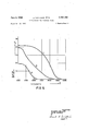
- FIG. compares the spectral sensitivity of the photocathode of the invention with several prior art cathodes.
- the quantum efficiencies are plotted along the ordinate as a function of the wavelength of the exciting light in A.
- the curve I was obtained with a monocrystal of cesium-activated gallum arsenide containing 4 10 atoms of zinc/cm. cleaved in a vacuum of torr.
- the curve II is typical of a Na KSb-Cs cathode
- the curve III is typical of a cathode Cs Sb.
- the gallium arsenide photocathode of the invention has a particularly favorable quantum efficiency, a very long-wave red boundary and a steeply ascending sensitivity curve.
- the light outputs for white light for the photocathodes associated with the curves I, II and III are approximately 450 a/lumen, 150 ,ua/lumen and 50 nah/lumen, respectively.
- a photocathode of an electron tube having an emissive surface portion comprising a p-type semiconductive material having an acceptor concentration of at least 1x10 atoms/cm. and selected from the group consisting of a III-V compound and mixed crystals of III-V compounds and having an energy gap between 1.1 and 1.6 electron volts and activated with an alkali metal, where III is an element selected from the group consisting of boron, aluminum, gallium, and indium, and V is an element selected from the group consisting of nitrogen, phosphorus, arsenic, and antimony.
Landscapes
- Common Detailed Techniques For Electron Tubes Or Discharge Tubes (AREA)
- Formation Of Various Coating Films On Cathode Ray Tubes And Lamps (AREA)
- Vessels And Coating Films For Discharge Lamps (AREA)
- Discharge Lamps And Accessories Thereof (AREA)
- Image-Pickup Tubes, Image-Amplification Tubes, And Storage Tubes (AREA)
Applications Claiming Priority (1)
| Application Number | Priority Date | Filing Date | Title |
|---|---|---|---|
| NL646413961A NL147572B (nl) | 1964-12-02 | 1964-12-02 | Elektrische ontladingsbuis met een fotokathode. |
Publications (1)
| Publication Number | Publication Date |
|---|---|
| US3387161A true US3387161A (en) | 1968-06-04 |
Family
ID=19791550
Family Applications (1)
| Application Number | Title | Priority Date | Filing Date |
|---|---|---|---|
| US508499A Expired - Lifetime US3387161A (en) | 1964-12-02 | 1965-11-18 | Photocathode for electron tubes |
Country Status (10)
| Country | Link |
|---|---|
| US (1) | US3387161A (de) |
| AT (1) | AT255506B (de) |
| BE (1) | BE673078A (de) |
| CH (1) | CH441527A (de) |
| DE (1) | DE1256808B (de) |
| DK (1) | DK120403B (de) |
| ES (1) | ES320158A1 (de) |
| GB (1) | GB1086228A (de) |
| NL (1) | NL147572B (de) |
| SE (1) | SE325968B (de) |
Cited By (15)
| Publication number | Priority date | Publication date | Assignee | Title |
|---|---|---|---|---|
| US3521073A (en) * | 1965-11-26 | 1970-07-21 | Gen Dynamics Corp | Light emitting semiconductor diode using the field emission effect |
| US3575628A (en) * | 1968-11-26 | 1971-04-20 | Westinghouse Electric Corp | Transmissive photocathode and devices utilizing the same |
| US3630587A (en) * | 1968-03-15 | 1971-12-28 | Philips Corp | Activating method for cesium activated iii-v compound photocathode using rare gas bombardment |
| US3631303A (en) * | 1970-01-19 | 1971-12-28 | Varian Associates | Iii-v cathodes having a built-in gradient of potential energy for increasing the emission efficiency |
| US3632442A (en) * | 1967-04-21 | 1972-01-04 | Philips Corp | Photocathodes |
| US3667007A (en) * | 1970-02-25 | 1972-05-30 | Rca Corp | Semiconductor electron emitter |
| US3699404A (en) * | 1971-02-24 | 1972-10-17 | Rca Corp | Negative effective electron affinity emitters with drift fields using deep acceptor doping |
| US3769536A (en) * | 1972-01-28 | 1973-10-30 | Varian Associates | Iii-v photocathode bonded to a foreign transparent substrate |
| US3845496A (en) * | 1973-09-10 | 1974-10-29 | Rca Corp | Infrared photocathode |
| US3958143A (en) * | 1973-01-15 | 1976-05-18 | Varian Associates | Long-wavelength photoemission cathode |
| US3960421A (en) * | 1972-03-27 | 1976-06-01 | U.S. Philips Corporation | Method of manufacturing a non-thermally emitting electrode for an electric discharge tube |
| US3986065A (en) * | 1974-10-24 | 1976-10-12 | Rca Corporation | Insulating nitride compounds as electron emitters |
| US4816183A (en) * | 1986-08-21 | 1989-03-28 | The Board Of Trustees Of The Leland Stanford Junior University | Composite photosensitive material |
| US5982093A (en) * | 1997-04-10 | 1999-11-09 | Hamamatsu Photonics K.K. | Photocathode and electron tube having enhanced absorption edge characteristics |
| US20060049755A1 (en) * | 2003-01-17 | 2006-03-09 | Takashi Watanabe | Alkali metal generating agent, alkali metal generator, photoelectric surface, secondary electron emission surface, electron tube, method for manufacturing photoelectric surface, method for manufacturing secondary electron emission surface, and method for manufacturing electron tube |
Families Citing this family (1)
| Publication number | Priority date | Publication date | Assignee | Title |
|---|---|---|---|---|
| JPH1196896A (ja) * | 1997-09-24 | 1999-04-09 | Hamamatsu Photonics Kk | 半導体光電面 |
Citations (2)
| Publication number | Priority date | Publication date | Assignee | Title |
|---|---|---|---|---|
| US3098168A (en) * | 1958-03-24 | 1963-07-16 | Csf | Hot electron cold lattice semiconductor cathode |
| US3114070A (en) * | 1957-12-16 | 1963-12-10 | Ass Elect Ind Manchester Ltd | Electron emitters |
-
1964
- 1964-12-02 NL NL646413961A patent/NL147572B/xx unknown
-
1965
- 1965-11-18 US US508499A patent/US3387161A/en not_active Expired - Lifetime
- 1965-11-27 DE DEN27690A patent/DE1256808B/de not_active Withdrawn
- 1965-11-29 SE SE15426/65A patent/SE325968B/xx unknown
- 1965-11-29 DK DK612865AA patent/DK120403B/da unknown
- 1965-11-29 CH CH1644965A patent/CH441527A/de unknown
- 1965-11-29 GB GB50530/65A patent/GB1086228A/en not_active Expired
- 1965-11-29 AT AT1070365A patent/AT255506B/de active
- 1965-11-30 ES ES0320158A patent/ES320158A1/es not_active Expired
- 1965-11-30 BE BE673078A patent/BE673078A/xx unknown
Patent Citations (2)
| Publication number | Priority date | Publication date | Assignee | Title |
|---|---|---|---|---|
| US3114070A (en) * | 1957-12-16 | 1963-12-10 | Ass Elect Ind Manchester Ltd | Electron emitters |
| US3098168A (en) * | 1958-03-24 | 1963-07-16 | Csf | Hot electron cold lattice semiconductor cathode |
Cited By (16)
| Publication number | Priority date | Publication date | Assignee | Title |
|---|---|---|---|---|
| US3521073A (en) * | 1965-11-26 | 1970-07-21 | Gen Dynamics Corp | Light emitting semiconductor diode using the field emission effect |
| US3632442A (en) * | 1967-04-21 | 1972-01-04 | Philips Corp | Photocathodes |
| US3630587A (en) * | 1968-03-15 | 1971-12-28 | Philips Corp | Activating method for cesium activated iii-v compound photocathode using rare gas bombardment |
| US3575628A (en) * | 1968-11-26 | 1971-04-20 | Westinghouse Electric Corp | Transmissive photocathode and devices utilizing the same |
| US3631303A (en) * | 1970-01-19 | 1971-12-28 | Varian Associates | Iii-v cathodes having a built-in gradient of potential energy for increasing the emission efficiency |
| US3667007A (en) * | 1970-02-25 | 1972-05-30 | Rca Corp | Semiconductor electron emitter |
| US3699404A (en) * | 1971-02-24 | 1972-10-17 | Rca Corp | Negative effective electron affinity emitters with drift fields using deep acceptor doping |
| US3769536A (en) * | 1972-01-28 | 1973-10-30 | Varian Associates | Iii-v photocathode bonded to a foreign transparent substrate |
| US3960421A (en) * | 1972-03-27 | 1976-06-01 | U.S. Philips Corporation | Method of manufacturing a non-thermally emitting electrode for an electric discharge tube |
| US3958143A (en) * | 1973-01-15 | 1976-05-18 | Varian Associates | Long-wavelength photoemission cathode |
| US3845496A (en) * | 1973-09-10 | 1974-10-29 | Rca Corp | Infrared photocathode |
| US3986065A (en) * | 1974-10-24 | 1976-10-12 | Rca Corporation | Insulating nitride compounds as electron emitters |
| US4816183A (en) * | 1986-08-21 | 1989-03-28 | The Board Of Trustees Of The Leland Stanford Junior University | Composite photosensitive material |
| US5982093A (en) * | 1997-04-10 | 1999-11-09 | Hamamatsu Photonics K.K. | Photocathode and electron tube having enhanced absorption edge characteristics |
| US20060049755A1 (en) * | 2003-01-17 | 2006-03-09 | Takashi Watanabe | Alkali metal generating agent, alkali metal generator, photoelectric surface, secondary electron emission surface, electron tube, method for manufacturing photoelectric surface, method for manufacturing secondary electron emission surface, and method for manufacturing electron tube |
| US7772771B2 (en) * | 2003-01-17 | 2010-08-10 | Hamamatsu Photonics K.K. | Alkali metal generating agent, alkali metal generator, photoelectric surface, secondary electron emission surface, electron tube, method for manufacturing photoelectric surface, method for manufacturing secondary electron emission surface, and method for manufacturing electron tube |
Also Published As
| Publication number | Publication date |
|---|---|
| DE1256808B (de) | 1967-12-21 |
| DK120403B (da) | 1971-05-24 |
| AT255506B (de) | 1967-07-10 |
| CH441527A (de) | 1967-08-15 |
| NL147572B (nl) | 1975-10-15 |
| BE673078A (de) | 1966-05-31 |
| ES320158A1 (es) | 1966-04-16 |
| GB1086228A (en) | 1967-10-04 |
| SE325968B (de) | 1970-07-13 |
| NL6413961A (de) | 1966-06-03 |
Similar Documents
| Publication | Publication Date | Title |
|---|---|---|
| US3387161A (en) | Photocathode for electron tubes | |
| US3814968A (en) | Solid state radiation sensitive field electron emitter and methods of fabrication thereof | |
| US3696262A (en) | Multilayered iii-v photocathode having a transition layer and a high quality active layer | |
| US3478213A (en) | Photomultiplier or image amplifier with secondary emission transmission type dynodes made of semiconductive material with low work function material disposed thereon | |
| Martinelli et al. | The application of semiconductors with negative electron affinity surfaces to electron emission devices | |
| US5354694A (en) | Method of making highly doped surface layer for negative electron affinity devices | |
| US3894332A (en) | Solid state radiation sensitive field electron emitter and methods of fabrication thereof | |
| US3644770A (en) | Photoemitter having a p-type semiconductive substrate overlaid with cesium and n-type cesium oxide layers | |
| Williams et al. | Current status of negative electron affinity devices | |
| US3575628A (en) | Transmissive photocathode and devices utilizing the same | |
| GB1299549A (en) | Aiii-bv cathodes having a built-in gradient of potential energy for increasing the emission efficiency | |
| US4639638A (en) | Photomultiplier dynode coating materials and process | |
| Escher et al. | Calculated energy distributions of electrons emitted from negative electron affinity GaAs: Cs–O surfaces | |
| US3197662A (en) | Transmissive spongy secondary emitter | |
| US3753023A (en) | Electron emissive device incorporating a secondary electron emitting material of antimony activated with potassium and cesium | |
| US4419603A (en) | Bialkaline photocathode having increased spectral sensitivity and method of manufacturing same | |
| US3986065A (en) | Insulating nitride compounds as electron emitters | |
| US3632442A (en) | Photocathodes | |
| Sommer | Practical use of III-V compound electron emitters | |
| US3408521A (en) | Semiconductor-type photocathode for an infrared device | |
| Miyazawa | Photoelectric Emission and Energy Structure of Cs3Sb | |
| US2254073A (en) | Photoelectrically sensitive surface | |
| US3858955A (en) | Method of making a iii-v compound electron-emissive cathode | |
| US4019082A (en) | Electron emitting device and method of making the same | |
| Simon et al. | GaAs1− xPx AS A NEW HIGH QUANTUM YIELD PHOTOEMISSIVE MATERIAL FOR THE VISIBLE SPECTRUM |