US3553489A - Phase sequence comparator - Google Patents
Phase sequence comparator Download PDFInfo
- Publication number
- US3553489A US3553489A US691474A US3553489DA US3553489A US 3553489 A US3553489 A US 3553489A US 691474 A US691474 A US 691474A US 3553489D A US3553489D A US 3553489DA US 3553489 A US3553489 A US 3553489A
- Authority
- US
- United States
- Prior art keywords
- pulses
- input
- gate
- pulse
- signal
- Prior art date
- Legal status (The legal status is an assumption and is not a legal conclusion. Google has not performed a legal analysis and makes no representation as to the accuracy of the status listed.)
- Expired - Lifetime
Links
- 238000000819 phase cycle Methods 0.000 title description 6
- 230000008859 change Effects 0.000 claims abstract description 8
- 238000004804 winding Methods 0.000 claims description 21
- 230000004044 response Effects 0.000 claims description 14
- 230000007704 transition Effects 0.000 claims description 3
- PCTMTFRHKVHKIS-BMFZQQSSSA-N (1s,3r,4e,6e,8e,10e,12e,14e,16e,18s,19r,20r,21s,25r,27r,30r,31r,33s,35r,37s,38r)-3-[(2r,3s,4s,5s,6r)-4-amino-3,5-dihydroxy-6-methyloxan-2-yl]oxy-19,25,27,30,31,33,35,37-octahydroxy-18,20,21-trimethyl-23-oxo-22,39-dioxabicyclo[33.3.1]nonatriaconta-4,6,8,10 Chemical compound C1C=C2C[C@@H](OS(O)(=O)=O)CC[C@]2(C)[C@@H]2[C@@H]1[C@@H]1CC[C@H]([C@H](C)CCCC(C)C)[C@@]1(C)CC2.O[C@H]1[C@@H](N)[C@H](O)[C@@H](C)O[C@H]1O[C@H]1/C=C/C=C/C=C/C=C/C=C/C=C/C=C/[C@H](C)[C@@H](O)[C@@H](C)[C@H](C)OC(=O)C[C@H](O)C[C@H](O)CC[C@@H](O)[C@H](O)C[C@H](O)C[C@](O)(C[C@H](O)[C@H]2C(O)=O)O[C@H]2C1 PCTMTFRHKVHKIS-BMFZQQSSSA-N 0.000 abstract description 5
- 101100321992 Drosophila melanogaster ABCD gene Proteins 0.000 abstract description 5
- 239000013598 vector Substances 0.000 description 5
- 230000001419 dependent effect Effects 0.000 description 3
- 238000010586 diagram Methods 0.000 description 3
- 230000001681 protective effect Effects 0.000 description 3
- 230000001052 transient effect Effects 0.000 description 2
- SVTBMSDMJJWYQN-UHFFFAOYSA-N 2-methylpentane-2,4-diol Chemical compound CC(O)CC(C)(C)O SVTBMSDMJJWYQN-UHFFFAOYSA-N 0.000 description 1
- 230000000694 effects Effects 0.000 description 1
- 230000004907 flux Effects 0.000 description 1
- 230000006870 function Effects 0.000 description 1
- 239000000463 material Substances 0.000 description 1
- 238000001208 nuclear magnetic resonance pulse sequence Methods 0.000 description 1
- 230000009993 protective function Effects 0.000 description 1
- 229910000859 α-Fe Inorganic materials 0.000 description 1
Images

Classifications
-
- H—ELECTRICITY
- H02—GENERATION; CONVERSION OR DISTRIBUTION OF ELECTRIC POWER
- H02H—EMERGENCY PROTECTIVE CIRCUIT ARRANGEMENTS
- H02H11/00—Emergency protective circuit arrangements for preventing the switching-on in case an undesired electric working condition might result
- H02H11/004—Emergency protective circuit arrangements for preventing the switching-on in case an undesired electric working condition might result in case of incorrect phase sequence; with switching for obtaining correct phase sequence
-
- G—PHYSICS
- G01—MEASURING; TESTING
- G01R—MEASURING ELECTRIC VARIABLES; MEASURING MAGNETIC VARIABLES
- G01R29/00—Arrangements for measuring or indicating electric quantities not covered by groups G01R19/00 - G01R27/00
- G01R29/18—Indicating phase sequence; Indicating synchronism
-
- H—ELECTRICITY
- H02—GENERATION; CONVERSION OR DISTRIBUTION OF ELECTRIC POWER
- H02H—EMERGENCY PROTECTIVE CIRCUIT ARRANGEMENTS
- H02H3/00—Emergency protective circuit arrangements for automatic disconnection directly responsive to an undesired change from normal electric working condition with or without subsequent reconnection ; integrated protection
- H02H3/38—Emergency protective circuit arrangements for automatic disconnection directly responsive to an undesired change from normal electric working condition with or without subsequent reconnection ; integrated protection responsive to both voltage and current; responsive to phase angle between voltage and current
- H02H3/382—Emergency protective circuit arrangements for automatic disconnection directly responsive to an undesired change from normal electric working condition with or without subsequent reconnection ; integrated protection responsive to both voltage and current; responsive to phase angle between voltage and current involving phase comparison between current and voltage or between values derived from current and voltage
-
- H—ELECTRICITY
- H03—ELECTRONIC CIRCUITRY
- H03K—PULSE TECHNIQUE
- H03K5/00—Manipulating of pulses not covered by one of the other main groups of this subclass
- H03K5/22—Circuits having more than one input and one output for comparing pulses or pulse trains with each other according to input signal characteristics, e.g. slope, integral
- H03K5/26—Circuits having more than one input and one output for comparing pulses or pulse trains with each other according to input signal characteristics, e.g. slope, integral the characteristic being duration, interval, position, frequency, or sequence
Definitions
- the comparator comprises two bistable devices each having a first input connected in common to receive the signal A from one input stage and the signal D from another input stage.
- One of the devices has a second input for receiving the signal B and the other device has a second input for receiving the signal C.
- the present invention consists in a sequence comparator for sensing the sequence of a plurality of input signals applied thereto in succession, comprising at least two bistable devices each having a first input connected to receive both a first and a second one of said signals, and a second input for receiving a further one of said signals, the further signals applied to the bistable devices being different from one another, and detector means for detecting a coincident change of state in all the devices in response to the said second signals applied thereto.
- the input signals may conveniently be pulses derived from different sinusoidal input quantities at predetermined instants together with the said second signal, an output being developed from the gate only in response to coincidence between all its input signals, these signals being either all positive in polarity or all negative.
- This output from the AND gate may be utilized to effect a protective function.
- the outputs from the comparators may be applied in common to detector means comprising two AND gates, one of which is arranged to produce an output in response to coincident pulses of one polarity and the other being arranged to produce an output in response to coincident pulses of the opposite polarity, the outputs from the two' gates themselves being applied to a further AND gate after having been extended for a predetermined period.
- This invention is of particular utility in protective relays in sensing the sequence of four vector quantities of the form described in our Pat. No. 1,096,279, i.e. the two vectors which define limiting conditions of operation for the relay (corresponding to the first and second signals referred to above), and two further vectors one of which is dependent on the impedance of the protected system and the other being dependent on both the impedance of the system and a vectorial quantity having a predetermined magnitude and phase angle which may conveniently define a distance boundary for distance protective relays.
- two bistable devices will be employed, the further signal applied to one device being determined by one of the aforesaid further vectors and the further signal applied to the other device being determined by the other vector.
- the occurrence of these two further signals in either order between the two limiting" signals is indicative of a fault within the system, and appropriate protective action may be taken in response to these conditions.
- FIG. 1 illustrates a bistable device in the form of a magnetic core having input and output windings employed in a comparator according to this invention
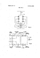
- FIG. 2 illustrates a block diagram of a phase sequence comparator according to this invention
- FIG. 3 illustrates a circuit diagram of one form of AND gate employed for detecting coincidence
- FIG. 4 illustrates a block diagram of another phase sequence comparator according to this invention.
- pulses A, B, C and D are initially produced from the sinusoidal signals at the instant of their transition from one polarity to another, Le. a positive pulse is produced as each signal goes positive and a negative pulse is produced as each signal goes negative.
- the vectorial quantities represented by pulses A and D will be regarded as the limiting values referred to above and the quantities B and C may appear in either one order or the other between them, and if comparison is to be effected on both the positive pulses and the negative pulses in the same circuit element then these limiting pulses A and D must not be spaced apart by more than Since the pulses B and C may arrive in either order, then the comparison may be effected separately, i.e.
- FIG. 1 there is shown a comparator in the form of a magnetic core. More particularly the core is in the form of a ferrite ring 1 upon which are wound two input windings 2 and 3 and an output or sense" winding 4, the winding 2 being arranged to receive the pulses A and D and the winding 3 being arranged to receive the pulse B.
- the material of the core possesses a squareloop characteristic and assuming that the sequence of the pulses is ABD then the initial positive pulse A on winding 2 will set" the magnetic state of the core, the following pulse B on winding 3 will reverse the state of the core causing a flux change through the output winding 4 thereby producing a pulse of one polarity and the subsequent pulse D on winding 2 will again reverse" the state of the core causing a pulse of the opposite polarity to be induced in the windirig 4. Following this, the negative pulses ABD occur in that sequence so that the state of the core continually changes with the application of each pulse.
- the core is thus operative as a bistable device with its operational state changing in synchronism with the application of the input pulses when these are applied in the correct sequence.
- the comparator may comprise any bistable device, e.g. an Eccles-Jordan-type trigger circuit with the pulses A and D applied to one input and the pulse B applied to the other input.
- an identical comparator is also employed for detecting the sequence of pulses ACD and, provided that the sequences of pulses ABD and ACD are in the correct order there will always be coincident output pulses from the two comparators upon the application of pulse D (as also will be the case for all the pulses A following the initial one).
- FIG. 2 there is shown one form of logical circuit for detecting this coincidence.
- This circuit comprises four input stages 5 to 8 for generating pulses A to D, respectively, two isolating stages 9 and 10 for preventing pulses A and D from interacting with their dif ferent sources, two comparators l1 and 12 of the type described and an AND gate 13.
- the comparator 11 receives the pulses A and D from the isolating stage 9 and receives the pulse B from its input stage 6. If the pulses ABD are received in the correct sequence a train of output pulses coincident with the input pulses will be applied to one input of the AND gate 13.
- the comparator l2 receives the pulses A and D from the isolating stage 10 and receives the pulse C from its input stage 7.
- the pulses A to D occur with both positive and negative polarity, and the AND gate must accommodate both types of .pulse.
- One form of gate which may be employed for this purpose is shown in FIG. 3.
- this gate comprises two sets of three series-connected NPN transistors A, B; 16A, B; and 17A, B, having a common collector load resistor 18, with the correspondingpairs of transistors having their base electrodes connectedbetween three center tapped windings 20, 21 and 22, respectively.
- the winding 20 has developed across it the output from the comparator 11
- the winding 21 has developed across it the output from the comparator 12
- the winding 22 has developed across it the D gating pulse from the input circuit 8.
- the windings 20 and 21 may constitute the output winding 3, center tapped.
- the operating time required to detect the occurrence of the pulses A to D in either of the two sequence referred to is minimized and although only one'polarity of these pulses need be considered for detecting a particular sequence the operating time could be up to twice as longas the previous case.
- the operation effected in response to pulse of only one polarity, i.e. one-half cycle of the sinusoidal wave errors due to transient components may be introduced, and in order to avoid this the operation must be dependent on an output being obtained from both positive and negative pulses, i.e. covering a full cycle of the wave, so that transient errors are balanced out.
- FIG. 4 A circuit which responds only to both polarities of pulses being in the particular sequences is shown in FIG. 4 and in this circuit those elements which perform the same function as those referred to in FIG. 2 have been identified by the same reference numeralsjln this case, the output from the ABD comparator 11 is applied to both an AND gate 24 and an AND gate 25, and similarly, the output from the ACD comparator 12 is applied to both AND gates, the two AND gates, the two additionally receiving a D pulse input from the input stage 8.
- the AND gate 24 however is designed to respond only to positive coincidence pulses whereas AND gate 25 responds only to negative coincidence pulses.
- pulses stretching circuits are arranged to extend the pulse lengths by a period equal to at least half a cycle so as to ensure coincidence at the AND gate 28, and thus an output, in response to either input pulse sequence ABCD or ACBD.
- a circuit for determining whether all of a plurality of phase signals on separate lines appear between two reference signals comprising a respective bistable circuit for each phase signal which is set to the same state by both the reference signals and to the opposite state by the respective phase signal, and gating means fed from all the bistable devices and with the second reference signal and effective to produce an output only when the second reference signal appears and all the bistable circuits change state together.
- each bistable circuit being set to one or the other state depending on the polarity of the pulse setting it.
- the gating means comprises two parallel strings of transistors, having collector, base and emitter electrodes, the transistors in each string having series-connected collector-emitter paths, a common load resistor for said transistors, and a plurality of commonly center tapped windings respectively coupled to receive the outputs from the bistable devices and the second reference signal, the base electrodes of corresponding transistors being connected together through these windings.
- the gating means comprises two AND gates, each gate having a plurality of inputs respectively connected to the corresponding outputs from all the bistable devices and a further input for receiving the second reference signal, an output being developed from one of the AND gates in response to coincident pulses of one polarity at all its inputs and an output being developed from the other AND gate in response to coincident pulses ofthe opposite polarity at all its inputs.
- bistable devices are magnetic cores.
Landscapes
- Physics & Mathematics (AREA)
- General Physics & Mathematics (AREA)
- Nonlinear Science (AREA)
- Manipulation Of Pulses (AREA)
- Safety Devices In Control Systems (AREA)
Applications Claiming Priority (1)
| Application Number | Priority Date | Filing Date | Title |
|---|---|---|---|
| GB56442/66A GB1168458A (en) | 1966-12-16 | 1966-12-16 | Signal sequence discriminator |
Publications (1)
| Publication Number | Publication Date |
|---|---|
| US3553489A true US3553489A (en) | 1971-01-05 |
Family
ID=10476629
Family Applications (1)
| Application Number | Title | Priority Date | Filing Date |
|---|---|---|---|
| US691474A Expired - Lifetime US3553489A (en) | 1966-12-16 | 1967-12-18 | Phase sequence comparator |
Country Status (4)
| Country | Link |
|---|---|
| US (1) | US3553489A (fr) |
| CH (1) | CH470669A (fr) |
| DE (1) | DE1591884A1 (fr) |
| GB (1) | GB1168458A (fr) |
Cited By (3)
| Publication number | Priority date | Publication date | Assignee | Title |
|---|---|---|---|---|
| US3744029A (en) * | 1969-04-25 | 1973-07-03 | Atlas Copco Ab | Programmable sequential control means having a plurality of control circuits for controlling a respective plurality of discrete suboperations |
| US4107616A (en) * | 1976-01-22 | 1978-08-15 | M. L. Engineering (Plymouth) Limited | Signal monitoring circuit |
| US4218658A (en) * | 1977-10-17 | 1980-08-19 | Moeller Charles R | Non-contemporaneous logic element and method for synthesizing a condition which represents a sequence |
Citations (3)
| Publication number | Priority date | Publication date | Assignee | Title |
|---|---|---|---|---|
| DE1161313B (de) * | 1961-11-23 | 1964-01-16 | Rotax Ltd | Elektronische Schaltung zum zeitlichen Trennen von gleichzeitig an zwei Eingaengen auftretenden Impulsen |
| US3287495A (en) * | 1965-04-12 | 1966-11-22 | David S Willard | Apparatus for elimination of noise and faint objects from a video signal |
| US3427601A (en) * | 1964-07-24 | 1969-02-11 | Sperry Rand Corp | Detector system and device |
-
1966
- 1966-12-16 GB GB56442/66A patent/GB1168458A/en not_active Expired
-
1967
- 1967-12-13 CH CH1748067A patent/CH470669A/fr not_active IP Right Cessation
- 1967-12-15 DE DE19671591884 patent/DE1591884A1/de active Pending
- 1967-12-18 US US691474A patent/US3553489A/en not_active Expired - Lifetime
Patent Citations (3)
| Publication number | Priority date | Publication date | Assignee | Title |
|---|---|---|---|---|
| DE1161313B (de) * | 1961-11-23 | 1964-01-16 | Rotax Ltd | Elektronische Schaltung zum zeitlichen Trennen von gleichzeitig an zwei Eingaengen auftretenden Impulsen |
| US3427601A (en) * | 1964-07-24 | 1969-02-11 | Sperry Rand Corp | Detector system and device |
| US3287495A (en) * | 1965-04-12 | 1966-11-22 | David S Willard | Apparatus for elimination of noise and faint objects from a video signal |
Cited By (3)
| Publication number | Priority date | Publication date | Assignee | Title |
|---|---|---|---|---|
| US3744029A (en) * | 1969-04-25 | 1973-07-03 | Atlas Copco Ab | Programmable sequential control means having a plurality of control circuits for controlling a respective plurality of discrete suboperations |
| US4107616A (en) * | 1976-01-22 | 1978-08-15 | M. L. Engineering (Plymouth) Limited | Signal monitoring circuit |
| US4218658A (en) * | 1977-10-17 | 1980-08-19 | Moeller Charles R | Non-contemporaneous logic element and method for synthesizing a condition which represents a sequence |
Also Published As
| Publication number | Publication date |
|---|---|
| CH470669A (fr) | 1969-03-31 |
| DE1591884A1 (de) | 1971-01-14 |
| GB1168458A (en) | 1969-10-29 |
Similar Documents
| Publication | Publication Date | Title |
|---|---|---|
| US3890544A (en) | Means for limiting the dynamic overreach in, for example, an impedance relay | |
| US2866092A (en) | Information processing device | |
| GB1272262A (en) | Detecting faults in electrical transmission lines | |
| GB784541A (en) | Improvements in or relating to magnetic switching circuits | |
| US3469196A (en) | Electrical signal phase comparator | |
| US3369156A (en) | Line distance protective device utilising ultra-rapid static relays | |
| GB1312643A (en) | High voltage electric circuit breakers | |
| GB1442812A (en) | Devices for monitoring electrical loads | |
| US3553489A (en) | Phase sequence comparator | |
| US3519884A (en) | Electrical protective relays | |
| GB1370180A (en) | Apparatus for fault testing binary circuit subsystems | |
| US3441745A (en) | Apparatus for frequency and phase comparison of two periodic signals | |
| GB1106843A (en) | Apparatus for correcting timing errors in television signals | |
| US3641443A (en) | Frequency compensated pulse time discriminator | |
| US3475655A (en) | Method and means for protecting an ac electric system from short circuits by a distance relay having quadrilateral characteristics | |
| US3009107A (en) | Electrical phase angle comparators | |
| US3986128A (en) | Phase selective device | |
| US3192323A (en) | Telephone system detection circuit | |
| US3233112A (en) | Preference circuit employing magnetic elements | |
| SU1647738A1 (ru) | Устройство дл выбора поврежденной фазы трехфазной линии электропередачи | |
| SU1003227A1 (ru) | Реле направлени мощности | |
| US3382372A (en) | Protective apparatus | |
| US3266017A (en) | Plural electrical paths monitored by comparison of transients | |
| US3371216A (en) | Protective apparatus | |
| SU1628228A1 (ru) | Статический определитель |