US3660682A - Current limiting circuit - Google Patents
Current limiting circuit Download PDFInfo
- Publication number
- US3660682A US3660682A US111217A US3660682DA US3660682A US 3660682 A US3660682 A US 3660682A US 111217 A US111217 A US 111217A US 3660682D A US3660682D A US 3660682DA US 3660682 A US3660682 A US 3660682A
- Authority
- US
- United States
- Prior art keywords
- voltage
- transistor
- resistor
- resistors
- current
- Prior art date
- Legal status (The legal status is an assumption and is not a legal conclusion. Google has not performed a legal analysis and makes no representation as to the accuracy of the status listed.)
- Expired - Lifetime
Links
Images
Classifications
-
- H—ELECTRICITY
- H03—ELECTRONIC CIRCUITRY
- H03G—CONTROL OF AMPLIFICATION
- H03G11/00—Limiting amplitude; Limiting rate of change of amplitude
- H03G11/002—Limiting amplitude; Limiting rate of change of amplitude without controlling loop
-
- H—ELECTRICITY
- H04—ELECTRIC COMMUNICATION TECHNIQUE
- H04Q—SELECTING
- H04Q1/00—Details of selecting apparatus or arrangements
- H04Q1/18—Electrical details
- H04Q1/30—Signalling arrangements; Manipulation of signalling currents
Definitions
- the disclosure includes a transistor connected in the signal ap- ..307/237, 307/297 plying path telephone trunk circuit
- the transistor IS Com I 58] Fie'ld 'g 307/296 297 237 nected into a circuit configuration of resistors to operate as a voltage controlled negative-resistance shunted by the resistors which absorb the excess power during adverse line con- [56] References Cited ditions.
- the overall voltage-current circuit characteristics UNITED STATES PATENTS very closely approximate the traditional ballast lamp.
- ballast lamp to compensate for the differences in the interconnecting cable resistances and the differences in the signaling equipment, as well as for possible signaling path faults.
- This type of ballast lamp operates by increasing its resistance as the current through it increases. The increased power dissipation in the lamp causes the resistance element to reach comparatively high temperatures and as a consequence a rather large bulb is used to enclose it.
- the presently available tungsten filament ballast lamp is not rugged, lacks long term reliability and exhibits a response lag that may permit injury to sensitive electronic equipment before its resistance reaches a value sufficient to limit the Current through it.
- Constant current transistor circuit are available that can limit the maximum current therethrough but, these constant current circuits utilize only a transistor or a group of transistors as the series limiting elements, and as a consequence, the power is dissipated in the transistor. This then requires that the transistors be large and be provided with heat sinks to dissipate heat generated by the transistors, thus defeating the space gains made possible by the use of transistors.
- a main object of the invention is to provide a current limiting device of compact form.
- Another object of the invention is to provide a current limiting device having the characteristics of the conventional ballast lamp.
- Still another object of the invention is to provide a transistorized current limiting device in which the transistor dissipates the minimum amount of power consistent with good regulations.
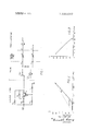
- FIG. 1 is a schematic circuit diagram of an illustrative embodiment of the current-limiting circuit of this invention.
- FIG. 2 is a characteristic curve illustrating the voltage-current characteristics of the circuit
- FIG. 3 is a characteristic curve illustrating the voltage-current characteristics of the transistor of the circuit.
- FIG. 1 shows the current limiting circuit connected in series from a telephone exchange signaling battery source of 50 volts through a trunk circuit signaling control to the M terminal of the trunk circuit.
- the signal path then normally extends via a signal conductor to a remote office trunk circuit where it is terminated on a terminal designated E.
- E This is the path over which the'remote office receives signals from the sending office.
- the E" terminal is normally connected to a battery potential via a signal receiving relay.
- a variation of this signaling system is disclosed in U.S. Pat. No. 2,744,963 where the signaling is performed via a set of composite equipment to economize on line conductors.
- the transistor Q1 operates as a voltage controlled negative-resistance" shunted by a resistor, that is, as the voltage at the collector terminal increases (due to a shorted or grounded signal line) the collector current decreases in equal and opposite proportion to the increase in current through resistor R4.
- the total current to the line remains constant.
- resistors R1 and R2 to the 50 volt potential.
- the potential at the junction of resistors R1 and R2 to the base of the transistor is such that with the emitter resistor R3 the transistor circuit is similar to a conventional constant current source.
- the position of resistor R4 across the emitter and collector terminals of the transistor Q1 causes the transistor to pass less current as the voltage at its collector terminal increases, since there is a greater voltage drop across the resistor network of R3 and R4, thus changing the positive voltage at the emitter terminal of Q1.
- the voltage at the base remains comparatively unchanged; however as the voltage at the emitter is increased, less current flows through the base emitter junction and thus decreases the current flow through the collector to provide a negative resistance effect.
- the transistor operates as a voltage controlled negative-resistance shunted by an effective resistance of about I54 ohms. This negative-resistance characteristic can be seen on FIG. 3. It can be seen that this Combination yields an effective and stable circuit with a characteristic closely approximating that of the ballast lamp.
- the voltage current characteristic curve of thev device is shownon FIG. 2 by the curved line to the right.
- the line from the zero point and intersecting the line of the device characteristic is the characteristic of a linear resistor (the network of R3, R4 and R5).
- the horizontal distance between these two lines at any voltage level represents the increment of current that the transistor must supply beyond that of the shunt resistor.
- said second voltage divider connected in i series between said DC voltage source negative terminal and said DC voltage source positive terminal, a transistor having base, collector and emitter electrodes, said collecto lec'trode' connected to said output terminal, said emitter elect de connected to the junction of said first and second resistors of said age drop across the resistors remains substantially constant, and said first voltage divider resistors have such a value that the voltage drop across the second resistor increases with increasing load current, said transistor operated by said increased voltage across said second resistor to conduct less current.
Landscapes
- Engineering & Computer Science (AREA)
- Computer Networks & Wireless Communication (AREA)
- Direct Current Feeding And Distribution (AREA)
Applications Claiming Priority (1)
| Application Number | Priority Date | Filing Date | Title |
|---|---|---|---|
| US11121771A | 1971-02-01 | 1971-02-01 |
Publications (1)
| Publication Number | Publication Date |
|---|---|
| US3660682A true US3660682A (en) | 1972-05-02 |
Family
ID=22337228
Family Applications (1)
| Application Number | Title | Priority Date | Filing Date |
|---|---|---|---|
| US111217A Expired - Lifetime US3660682A (en) | 1971-02-01 | 1971-02-01 | Current limiting circuit |
Country Status (4)
| Country | Link |
|---|---|
| US (1) | US3660682A (fr) |
| BE (1) | BE778687A (fr) |
| CA (1) | CA934010A (fr) |
| IT (1) | IT946751B (fr) |
Cited By (3)
| Publication number | Priority date | Publication date | Assignee | Title |
|---|---|---|---|---|
| US4377842A (en) * | 1980-10-06 | 1983-03-22 | International Business Machines Corporation | Flyback voltage control |
| US4417280A (en) * | 1980-05-16 | 1983-11-22 | Fuji Photo Optical Co., Ltd. | Servo amplifier for television camera lens |
| US5489874A (en) * | 1992-12-28 | 1996-02-06 | Oki Electric Industry Co., Ltd. | Inverting amplifier having negative-resistance circuit |
Citations (2)
| Publication number | Priority date | Publication date | Assignee | Title |
|---|---|---|---|---|
| US3251951A (en) * | 1962-02-26 | 1966-05-17 | Philips Corp | Circuit for automatic adjustment of impedance of a telephone loop |
| FR1503948A (fr) * | 1966-10-19 | 1967-12-01 | Limiteur de courant à transistor |
-
1971
- 1971-02-01 US US111217A patent/US3660682A/en not_active Expired - Lifetime
- 1971-12-17 CA CA130391A patent/CA934010A/en not_active Expired
-
1972
- 1972-01-20 IT IT19601/72A patent/IT946751B/it active
- 1972-01-31 BE BE778687A patent/BE778687A/fr not_active IP Right Cessation
Patent Citations (2)
| Publication number | Priority date | Publication date | Assignee | Title |
|---|---|---|---|---|
| US3251951A (en) * | 1962-02-26 | 1966-05-17 | Philips Corp | Circuit for automatic adjustment of impedance of a telephone loop |
| FR1503948A (fr) * | 1966-10-19 | 1967-12-01 | Limiteur de courant à transistor |
Cited By (8)
| Publication number | Priority date | Publication date | Assignee | Title |
|---|---|---|---|---|
| US4417280A (en) * | 1980-05-16 | 1983-11-22 | Fuji Photo Optical Co., Ltd. | Servo amplifier for television camera lens |
| US4377842A (en) * | 1980-10-06 | 1983-03-22 | International Business Machines Corporation | Flyback voltage control |
| US5489874A (en) * | 1992-12-28 | 1996-02-06 | Oki Electric Industry Co., Ltd. | Inverting amplifier having negative-resistance circuit |
| US5498991A (en) * | 1992-12-28 | 1996-03-12 | Oki Electric Industry Co., Ltd. | Level shifter circuit |
| US5504442A (en) * | 1992-12-28 | 1996-04-02 | Oki Electric Industry Co., Ltd. | Sense circuit |
| US5510746A (en) * | 1992-12-28 | 1996-04-23 | Oki Electric Industry Co., Ltd. | Load circuit tolerating large current and voltage swings |
| US5514986A (en) * | 1992-12-28 | 1996-05-07 | Oki Electric Industry Co., Ltd. | Sense circuit, memory circuit, negative-resistance circuit, schmitt trigger, load circuit, level shifter, and amplifier |
| US5519348A (en) * | 1992-12-28 | 1996-05-21 | Oki Electric Industry Co., Ltd. | Sense circuit, memory circuit, negative-resistance circuit, schmitt trigger, load circuit, level shifter, and amplifier |
Also Published As
| Publication number | Publication date |
|---|---|
| IT946751B (it) | 1973-05-21 |
| CA934010A (en) | 1973-09-18 |
| BE778687A (fr) | 1972-07-31 |
Similar Documents
| Publication | Publication Date | Title |
|---|---|---|
| US4176288A (en) | Zero voltage switching solid state relay | |
| US4158150A (en) | Solid state relay with zero crossover feature | |
| US3959713A (en) | Solid state current limit circuit | |
| US4158866A (en) | Protection circuit for transistorized switch | |
| US4086503A (en) | Control circuit initiating conduction of an opto-isolator unit | |
| US2848653A (en) | Transistor gating circuit | |
| US3240997A (en) | Power supply | |
| JPS6030140B2 (ja) | 電話機用回路 | |
| US3124697A (en) | Voltage regulating arrangement | |
| US3660682A (en) | Current limiting circuit | |
| EP0593588B1 (fr) | Agencement de protection de circuit | |
| US3109981A (en) | Over-voltage protective circuit | |
| US4789842A (en) | Composite transistor device with over-current protection | |
| US3084311A (en) | Time delay circuit | |
| JPS5814623A (ja) | 電気負荷の短絡保護装置 | |
| US4084070A (en) | Overcurrent protection circuit | |
| US3309583A (en) | Electronic device for the control of relays and similar apparatus | |
| US4567388A (en) | Clamp circuit | |
| SU1001056A1 (ru) | Устройство дл защиты стабилизатора напр жени | |
| SU1030780A1 (ru) | Стабилизатор напр жени с защитой | |
| SU1108418A2 (ru) | Устройство дл защиты стабилизатора напр жени | |
| US3097313A (en) | Rc-coupled monostable transistor circuit with diode shunt to provide fast recovery time | |
| SU1084770A2 (ru) | Компенсационный стабилизатор напр жени посто нного тока | |
| SU873390A1 (ru) | Устройство установки схем цифровой автоматики в исходное состо ние | |
| SU879572A1 (ru) | Стабилизатор посто нного напр жени |
Legal Events
| Date | Code | Title | Description |
|---|---|---|---|
| AS | Assignment |
Owner name: AG COMMUNICATION SYSTEMS CORPORATION, 2500 W. UTOP Free format text: ASSIGNMENT OF ASSIGNORS INTEREST.;ASSIGNOR:GTE COMMUNICATION SYSTEMS CORPORATION;REEL/FRAME:005060/0501 Effective date: 19881228 |