US4045745A - Low-frequency power amplifier - Google Patents
Low-frequency power amplifier Download PDFInfo
- Publication number
- US4045745A US4045745A US05/672,336 US67233676A US4045745A US 4045745 A US4045745 A US 4045745A US 67233676 A US67233676 A US 67233676A US 4045745 A US4045745 A US 4045745A
- Authority
- US
- United States
- Prior art keywords
- terminal
- voltage
- resistor
- inverting input
- transistors
- Prior art date
- Legal status (The legal status is an assumption and is not a legal conclusion. Google has not performed a legal analysis and makes no representation as to the accuracy of the status listed.)
- Expired - Lifetime
Links
Images
Classifications
-
- H—ELECTRICITY
- H03—ELECTRONIC CIRCUITRY
- H03F—AMPLIFIERS
- H03F3/00—Amplifiers with only discharge tubes or only semiconductor devices as amplifying elements
- H03F3/30—Single-ended push-pull [SEPP] amplifiers; Phase-splitters therefor
- H03F3/3083—Single-ended push-pull [SEPP] amplifiers; Phase-splitters therefor the power transistors being of the same type
- H03F3/3086—Single-ended push-pull [SEPP] amplifiers; Phase-splitters therefor the power transistors being of the same type two power transistors being controlled by the input signal
- H03F3/3091—Single-ended push-pull [SEPP] amplifiers; Phase-splitters therefor the power transistors being of the same type two power transistors being controlled by the input signal comprising two complementary transistors for phase-splitting
-
- H—ELECTRICITY
- H03—ELECTRONIC CIRCUITRY
- H03F—AMPLIFIERS
- H03F1/00—Details of amplifiers with only discharge tubes, only semiconductor devices or only unspecified devices as amplifying elements
- H03F1/30—Modifications of amplifiers to reduce influence of variations of temperature or supply voltage or other physical parameters
- H03F1/307—Modifications of amplifiers to reduce influence of variations of temperature or supply voltage or other physical parameters in push-pull amplifiers
Definitions
- Our present invention relates to a low-frequency power amplifier of the operational type, with a noninverting and an inverting input terminal and with a feedback resistor inserted between its inverting input terminal and its output terminal.
- the gain of such an operational amplifier is determined, as is well known, by the ratio of the magnitude of the aforementioned feedback resistor to an external impedance inserted between the inverting input terminal and ground; as shown in the prior patent referred to, this external impedance may comprise another resistor in series with a condenser. If the capacitance of this condenser is large enough to be negligible in the range of operating (e.g. audio) frequencies of the amplifier, the amplification factor A is given by the well-known formula
- R 1 and R 2 respectively represent the internal feedback resistor and the external resistor in series therewith. Resistor R 1 , therefore, is generally made much larger than resistor R 2 .
- the second twin transistor of the voltage-stabilizing circuit draws current through the internal feedback resistor (referred to above as R 1 ) so that the voltage drop thereacross varies with the stabilizing current.
- R 1 the internal feedback resistor
- An object of our present invention is to provide simplified circuitry for a low-frequency power amplifier, or similar semiconductive devices, obviating the need for a separate terminal to be capacitively grounded in order to absorb supply-voltage fluctuations.
- Another object is to provide, in an amplifier of the general type disclosed in prior U.S. Pat. No. 3,828,265, a single external circuit for voltage-stabilizing and gain-controlling purposes.
- the voltage divider comprises a larger first resistance between the tap and the output terminal and a smaller resistance between the tap and the ground terminal.
- the magnitude of the internal feedback resistor (R 1 ) should substantially exceed the first resistance of the divider.
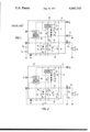
- FIG. 1 is a circuit diagram of a conventional power amplifier generally similar to that shown in prior U.S. Pat. No. 3,828,265;
- FIG. 2 is a circuit diagram showing the same kind of amplifier incorporating our present invention.
- FIG. 1 represents a simplified presentation of an amplifier of the type disclosed in U.S. Pat. No. 3,828,265, including a monolithic chip IC with a number of terminals 1- 6 giving access to its internal circuitry.
- That circuitry includes a transistorized amplification network with three cascaded stages, the first two stages being represented schematically by a block 10.
- the third or power stage includes a pair of NPN output transistors T 1 , T 2 serially connected between a live (positive) bus bar 11 and a ground bus bar 12, bus bar 11 being tied to terminal 5 for connection to a d-c power supply (not shown) delivering a voltage V S to the network; bus bar 12 is tied to terminal 2.
- Power transistors T 1 and T 2 are controlled, in respective Darlington connections, by a pair of pilot transistors T 6 and T 7 of opposite conductivity types (NPN and PNP, respectively); the bases of these pilot transistors are biased by an output lead 13 of a current-limiting circuit G (details of which are shown in the aforementioned patent) with interposition of a low resistance, in the form of three cascaded diodes D 1 - D 3 , between the bases of transistors T 6 and T 7 .
- a current-limiting circuit G (details of which are shown in the aforementioned patent) with interposition of a low resistance, in the form of three cascaded diodes D 1 - D 3 , between the bases of transistors T 6 and T 7 .
- the current flow in lead 13 is determined by the second or intermediate amplification stage in block 10, under the control of a signal applied to terminal 1 which constitutes the noninverting input of the amplifier, and is modified by a voltage-stabilizing circuit including an NPN transistor T 4 whose collector is connected to another output of circuit G via a lead 14.
- the emitter of transistor T 4 is grounded through a resistor R 5 while its base is tied to the collector of another NPN transistor T 3 with a grounded emitter; a twin T 5 of transistor T 3 , also with a grounded emitter, has its collector tied to terminal 3 which is the inverting input of the amplifier.
- the interconnected bases of twin transistors T 3 and T 5 are joined by way of a diode D 4 to the collector of transistor T 3 and thus to the base of transistor T 4 ; the current drawn by transistor T 5 substantially duplicates that drawn by its twin T 3 .
- a feedback resistor R 1 which like resistor R 5 forms part of the integrated chip IC, lies between inverting input terminal 3 and terminal 4 which constitutes the output of the amplifier and which feeds a load connected between this terminal and ground, the load being here shown as a microphone Z in series with a coupling condenser C 3 .
- resistors R 3 and R 4 Two other resistors R 3 and R 4 , also monolithically integrated in the chip IC, form a voltage divider connected between positive bus bar 11 and the collector of transistor T 3 .
- the junction of resistors R 3 and R 4 is tied to terminal 6 which is grounded for alternating current through a capacitor C 1 designed to smooth any fluctuations of supply voltage V S .
- Another external capacitor C 2 is inserted between ground and inverting input terminal 3 in series with an external resistor R 2 forming a gain-determining voltage divider with internal resistor R 1 as discussed above.
- the capacitance C 2 is negligible at the operating frequencies of the system but blocks the flow of direct current through resistor R 2 .
- FIG. 2 showing a generally similar power amplifier whose internal circuitry, within chip IC, differs from that shown in FIG. 1 by the omission of resistor R 4 and of the connection leading from resistor R 3 to an external capacitance C 1 via an ancillary terminal 6.
- Output terminal 4 furthermore, is grounded through a voltage divider consisting of resistors R 6 and R 7 in series; a tap on this voltage divider, i.e. the junction of its two resistors, is returned to inverting input terminal 3 through a capacitance C 4 .
- FIGS. 1 and 2 A comparison between FIGS. 1 and 2 shows that capacitance C 4 and resistor R 7 play the part of elements C 2 and R 2 of the conventional amplifier lying in series with feedback resistor R 1 .
- resistor R 7 in FIG. 2 determines the amplification factor A according to equation (1), it being therefore desirable that R 1 be considerably larger than R 7 .
- ⁇ I 5 is the fluctuation of the collector current of transistor T 5 due to a fluctuation ⁇ V S of the supply voltage V S .
- terminal 3 is linked with terminal 4 by two essentially resistive parallel branches R 1 , R 6 and is grounded through resistor R 7 .
- R 1 > R 6 the ratio between an input voltage V i at terminal 1 (which is essentially duplicated at terminal 3) and the corresponding output voltage V 0 is given by ##EQU3## whence the amplification factor A is given by ##EQU4##
- the gain of the amplifier of FIG. 2 is determined by two external resistance elements R 6 and R 7 which can be easily adjusted to the desired values independently of the circuit constants of chip IC.
- our improved amplifier may be mounted on a socket or supporting strip with five terminals (including ground terminal 2) from which the external connections can be extended with the aid of a 5-tongue lead frame of the type described in commonly owned application Ser. No. 508,951 filed Sept. 23, 1974 by Raimondo Paletto.
- Our present invention is not limited to a power amplifier of the type discussed but is applicable to other semiconductive devices, especially those of the integrated-circuit type, in which fluctuations of a supply voltage are to be compensated to minimize their effect upon the output of an amplification stage.
Landscapes
- Engineering & Computer Science (AREA)
- Power Engineering (AREA)
- Amplifiers (AREA)
Applications Claiming Priority (2)
| Application Number | Priority Date | Filing Date | Title |
|---|---|---|---|
| IT21984/75A IT1034831B (it) | 1975-04-04 | 1975-04-04 | Amplificatore di potenza in bassa frequenza in circuito integrato monolitico con circutto esterno combinato per la reiezione alla linea e la determinazione del guadagno |
| IT21984/75 | 1975-04-04 |
Publications (1)
| Publication Number | Publication Date |
|---|---|
| US4045745A true US4045745A (en) | 1977-08-30 |
Family
ID=11189774
Family Applications (1)
| Application Number | Title | Priority Date | Filing Date |
|---|---|---|---|
| US05/672,336 Expired - Lifetime US4045745A (en) | 1975-04-04 | 1976-03-31 | Low-frequency power amplifier |
Country Status (7)
| Country | Link |
|---|---|
| US (1) | US4045745A (pt) |
| JP (1) | JPS51123043A (pt) |
| BR (1) | BR7601998A (pt) |
| DE (1) | DE2613761C3 (pt) |
| FR (1) | FR2306567A1 (pt) |
| GB (1) | GB1528068A (pt) |
| IT (1) | IT1034831B (pt) |
Cited By (2)
| Publication number | Priority date | Publication date | Assignee | Title |
|---|---|---|---|---|
| US4278540A (en) * | 1979-05-17 | 1981-07-14 | Mordeki Drori | Back washing fluid filters |
| US20040227055A1 (en) * | 2003-05-09 | 2004-11-18 | Peter Hausberger | Device for the reading-out and/or testing of matrices or optical storage media |
Families Citing this family (1)
| Publication number | Priority date | Publication date | Assignee | Title |
|---|---|---|---|---|
| JP3258906B2 (ja) * | 1995-08-09 | 2002-02-18 | ローム株式会社 | オーディオ信号増幅装置 |
Citations (3)
| Publication number | Priority date | Publication date | Assignee | Title |
|---|---|---|---|---|
| DE1259952B (de) * | 1965-10-29 | 1968-02-01 | Audison Vertriebs G M B H | Transistorisierter Niederfrequenzverstaerker fuer hohe Ausgangsleistungen mit einer transformatorlosen Komplementaer-Gegentakt-Endstufe |
| GB1202461A (en) * | 1968-03-29 | 1970-08-19 | Rank Organisation Ltd | Power amplifiers with complementary pair driver stages |
| US3828265A (en) * | 1971-02-05 | 1974-08-06 | Ates Componenti Elettron | Low frequency power amplifier |
Family Cites Families (5)
| Publication number | Priority date | Publication date | Assignee | Title |
|---|---|---|---|---|
| DE1135959B (de) * | 1961-05-25 | 1962-09-06 | Rohde & Schwarz | Schaltungsanordnung zum Einfuehren einer Gegenkopplung bei einem Verstaerker |
| US3376515A (en) * | 1965-03-05 | 1968-04-02 | William G. Dilley | Single-ended, push-pull transistor audio amplifier |
| US3550030A (en) * | 1968-11-29 | 1970-12-22 | Abex Corp | Transient regulation of direct current electrical power supplies |
| DE1927496C3 (de) * | 1969-05-30 | 1980-01-03 | Gorenje Koerting Electronic Gmbh & Co, 8217 Grassau | Selektiver Transistorverstärker für amplitudenmodulierte Schwingungen |
| NL165617C (nl) * | 1974-12-18 | 1981-04-15 | Philips Nv | Televisiebeeldweergeefinrichting met een video- versterker. |
-
1975
- 1975-04-04 IT IT21984/75A patent/IT1034831B/it active
-
1976
- 1976-03-31 US US05/672,336 patent/US4045745A/en not_active Expired - Lifetime
- 1976-03-31 DE DE2613761A patent/DE2613761C3/de not_active Expired
- 1976-04-02 BR BR7601998A patent/BR7601998A/pt unknown
- 1976-04-02 GB GB13417/76A patent/GB1528068A/en not_active Expired
- 1976-04-02 FR FR7609637A patent/FR2306567A1/fr active Granted
- 1976-04-03 JP JP51037708A patent/JPS51123043A/ja active Pending
Patent Citations (3)
| Publication number | Priority date | Publication date | Assignee | Title |
|---|---|---|---|---|
| DE1259952B (de) * | 1965-10-29 | 1968-02-01 | Audison Vertriebs G M B H | Transistorisierter Niederfrequenzverstaerker fuer hohe Ausgangsleistungen mit einer transformatorlosen Komplementaer-Gegentakt-Endstufe |
| GB1202461A (en) * | 1968-03-29 | 1970-08-19 | Rank Organisation Ltd | Power amplifiers with complementary pair driver stages |
| US3828265A (en) * | 1971-02-05 | 1974-08-06 | Ates Componenti Elettron | Low frequency power amplifier |
Cited By (2)
| Publication number | Priority date | Publication date | Assignee | Title |
|---|---|---|---|---|
| US4278540A (en) * | 1979-05-17 | 1981-07-14 | Mordeki Drori | Back washing fluid filters |
| US20040227055A1 (en) * | 2003-05-09 | 2004-11-18 | Peter Hausberger | Device for the reading-out and/or testing of matrices or optical storage media |
Also Published As
| Publication number | Publication date |
|---|---|
| JPS51123043A (en) | 1976-10-27 |
| DE2613761A1 (de) | 1976-10-28 |
| BR7601998A (pt) | 1976-10-05 |
| IT1034831B (it) | 1979-10-10 |
| DE2613761B2 (de) | 1978-07-27 |
| GB1528068A (en) | 1978-10-11 |
| FR2306567A1 (fr) | 1976-10-29 |
| DE2613761C3 (de) | 1986-11-13 |
| FR2306567B1 (pt) | 1978-11-17 |
Similar Documents
| Publication | Publication Date | Title |
|---|---|---|
| US4586000A (en) | Transformerless current balanced amplifier | |
| US5323121A (en) | Folded cascode operational amplifier with gain enhancing base current compensation | |
| GB1470736A (en) | Amplifier circuit | |
| US3555309A (en) | Electrical circuits | |
| JP2869664B2 (ja) | 電流増幅器 | |
| JP2877315B2 (ja) | 低周波増幅器のための集積可能なab級出力段 | |
| US4045745A (en) | Low-frequency power amplifier | |
| US4425551A (en) | Differential amplifier stage having bias compensating means | |
| GB1513024A (en) | Amplifier circuit arrangement | |
| US3970947A (en) | Multi-stage differential amplifier circuit with means for compensating the temperature drift of a constant current source transistor | |
| US5115204A (en) | Differential amplifier | |
| US4017749A (en) | Transistor circuit including source voltage ripple removal | |
| US3262062A (en) | Direct current amplifier of the type comprising two cascaded transistors in series with a third transistor | |
| JPS5827411A (ja) | 差動増幅器回路 | |
| US5150073A (en) | Low-noise preamplifier stage, in particular for magnetic heads | |
| US4167708A (en) | Transistor amplifier | |
| US4293824A (en) | Linear differential amplifier with unbalanced output | |
| JP2694767B2 (ja) | 積分器 | |
| NO124403B (pt) | ||
| US5528683A (en) | Method and circuit for implementing an impedance, in particular for DC telephonic applications | |
| US4758798A (en) | Output amplifier | |
| JP2538013Y2 (ja) | ハイパスフィルタ回路 | |
| JPS646583Y2 (pt) | ||
| JP2577946B2 (ja) | 増幅回路 | |
| SU1626327A1 (ru) | Дифференциальный усилитель |