US4259145A - Ion source for reactive ion etching - Google Patents
Ion source for reactive ion etching Download PDFInfo
- Publication number
- US4259145A US4259145A US06/053,491 US5349179A US4259145A US 4259145 A US4259145 A US 4259145A US 5349179 A US5349179 A US 5349179A US 4259145 A US4259145 A US 4259145A
- Authority
- US
- United States
- Prior art keywords
- ion
- grid
- plasma
- etching
- apertures
- Prior art date
- Legal status (The legal status is an assumption and is not a legal conclusion. Google has not performed a legal analysis and makes no representation as to the accuracy of the status listed.)
- Expired - Lifetime
Links
- 238000001020 plasma etching Methods 0.000 title claims abstract description 18
- 150000002500 ions Chemical class 0.000 claims abstract description 89
- 238000010884 ion-beam technique Methods 0.000 claims abstract description 34
- 238000005530 etching Methods 0.000 claims abstract description 25
- 238000000605 extraction Methods 0.000 claims abstract description 12
- 239000000463 material Substances 0.000 claims abstract description 12
- 238000004544 sputter deposition Methods 0.000 claims abstract description 11
- 239000000126 substance Substances 0.000 claims abstract description 4
- 238000000034 method Methods 0.000 claims description 18
- 239000000758 substrate Substances 0.000 claims description 6
- 229910052710 silicon Inorganic materials 0.000 claims 1
- 239000010703 silicon Substances 0.000 claims 1
- 239000007787 solid Substances 0.000 claims 1
- 235000012431 wafers Nutrition 0.000 abstract description 19
- 230000001133 acceleration Effects 0.000 description 21
- 239000007789 gas Substances 0.000 description 14
- VYPSYNLAJGMNEJ-UHFFFAOYSA-N Silicium dioxide Chemical compound O=[Si]=O VYPSYNLAJGMNEJ-UHFFFAOYSA-N 0.000 description 12
- TXEYQDLBPFQVAA-UHFFFAOYSA-N tetrafluoromethane Chemical compound FC(F)(F)F TXEYQDLBPFQVAA-UHFFFAOYSA-N 0.000 description 8
- XKRFYHLGVUSROY-UHFFFAOYSA-N argon Substances [Ar] XKRFYHLGVUSROY-UHFFFAOYSA-N 0.000 description 6
- 229910052681 coesite Inorganic materials 0.000 description 6
- 229910052906 cristobalite Inorganic materials 0.000 description 6
- 230000009977 dual effect Effects 0.000 description 6
- 239000000377 silicon dioxide Substances 0.000 description 6
- 229910052682 stishovite Inorganic materials 0.000 description 6
- 229910052905 tridymite Inorganic materials 0.000 description 6
- 238000013461 design Methods 0.000 description 5
- 238000000992 sputter etching Methods 0.000 description 5
- 229910052786 argon Inorganic materials 0.000 description 4
- 238000003486 chemical etching Methods 0.000 description 3
- 238000001312 dry etching Methods 0.000 description 3
- 239000004065 semiconductor Substances 0.000 description 3
- XEEYBQQBJWHFJM-UHFFFAOYSA-N Iron Chemical compound [Fe] XEEYBQQBJWHFJM-UHFFFAOYSA-N 0.000 description 2
- PXHVJJICTQNCMI-UHFFFAOYSA-N Nickel Chemical compound [Ni] PXHVJJICTQNCMI-UHFFFAOYSA-N 0.000 description 2
- -1 argon ions Chemical class 0.000 description 2
- 238000005516 engineering process Methods 0.000 description 2
- 230000000873 masking effect Effects 0.000 description 2
- 230000007935 neutral effect Effects 0.000 description 2
- 238000004088 simulation Methods 0.000 description 2
- 229910004014 SiF4 Inorganic materials 0.000 description 1
- 238000013459 approach Methods 0.000 description 1
- 239000002131 composite material Substances 0.000 description 1
- 239000003989 dielectric material Substances 0.000 description 1
- 238000010494 dissociation reaction Methods 0.000 description 1
- 230000005593 dissociations Effects 0.000 description 1
- 238000009826 distribution Methods 0.000 description 1
- 230000000694 effects Effects 0.000 description 1
- 238000002474 experimental method Methods 0.000 description 1
- 230000003116 impacting effect Effects 0.000 description 1
- 230000006698 induction Effects 0.000 description 1
- 239000011261 inert gas Substances 0.000 description 1
- 239000011810 insulating material Substances 0.000 description 1
- 239000012212 insulator Substances 0.000 description 1
- 230000003993 interaction Effects 0.000 description 1
- 238000010849 ion bombardment Methods 0.000 description 1
- 239000005433 ionosphere Substances 0.000 description 1
- 239000005443 ionospheric plasma Substances 0.000 description 1
- 229910052742 iron Inorganic materials 0.000 description 1
- 239000000696 magnetic material Substances 0.000 description 1
- 238000004519 manufacturing process Methods 0.000 description 1
- 239000002184 metal Substances 0.000 description 1
- 229910052751 metal Inorganic materials 0.000 description 1
- 239000000203 mixture Substances 0.000 description 1
- 229910052759 nickel Inorganic materials 0.000 description 1
- 238000012545 processing Methods 0.000 description 1
- 238000005086 pumping Methods 0.000 description 1
- 238000005546 reactive sputtering Methods 0.000 description 1
- 238000011160 research Methods 0.000 description 1
- 238000000926 separation method Methods 0.000 description 1
- ABTOQLMXBSRXSM-UHFFFAOYSA-N silicon tetrafluoride Chemical compound F[Si](F)(F)F ABTOQLMXBSRXSM-UHFFFAOYSA-N 0.000 description 1
- 229910001220 stainless steel Inorganic materials 0.000 description 1
- 239000010935 stainless steel Substances 0.000 description 1
- 238000012360 testing method Methods 0.000 description 1
- XLYOFNOQVPJJNP-UHFFFAOYSA-N water Substances O XLYOFNOQVPJJNP-UHFFFAOYSA-N 0.000 description 1
- 238000007704 wet chemistry method Methods 0.000 description 1
Images

Classifications
-
- H—ELECTRICITY
- H01—ELECTRIC ELEMENTS
- H01J—ELECTRIC DISCHARGE TUBES OR DISCHARGE LAMPS
- H01J37/00—Discharge tubes with provision for introducing objects or material to be exposed to the discharge, e.g. for the purpose of examination or processing thereof
- H01J37/02—Details
- H01J37/04—Arrangements of electrodes and associated parts for generating or controlling the discharge, e.g. electron-optical arrangement or ion-optical arrangement
- H01J37/08—Ion sources; Ion guns
-
- H—ELECTRICITY
- H01—ELECTRIC ELEMENTS
- H01J—ELECTRIC DISCHARGE TUBES OR DISCHARGE LAMPS
- H01J27/00—Ion beam tubes
- H01J27/02—Ion sources; Ion guns
- H01J27/08—Ion sources; Ion guns using arc discharge
- H01J27/14—Other arc discharge ion sources using an applied magnetic field
-
- H—ELECTRICITY
- H01—ELECTRIC ELEMENTS
- H01J—ELECTRIC DISCHARGE TUBES OR DISCHARGE LAMPS
- H01J37/00—Discharge tubes with provision for introducing objects or material to be exposed to the discharge, e.g. for the purpose of examination or processing thereof
- H01J37/30—Electron-beam or ion-beam tubes for localised treatment of objects
- H01J37/305—Electron-beam or ion-beam tubes for localised treatment of objects for casting, melting, evaporating, or etching
- H01J37/3053—Electron-beam or ion-beam tubes for localised treatment of objects for casting, melting, evaporating, or etching for evaporating or etching
- H01J37/3056—Electron-beam or ion-beam tubes for localised treatment of objects for casting, melting, evaporating, or etching for evaporating or etching for microworking, e. g. etching of gratings or trimming of electrical components
Definitions
- the present invention relates to reactive ion beam etching processes, and more particularly to a method for providing a low energy ion beam of controlled energy and current density in the reactive ion etching of materials.
- Dry etching of semiconducting and insulating materials by reactive ions is of increasing importance in semiconductor technology as an improvement on wet chemical processes.
- Three aspects of the dry etching process are identified as follows:
- the main etching process used is almost entirely due to physical sputtering, usually by ions accelerated from a dual-grid ion source.
- the wafers to be etched are placed in a chamber of reactive gas (e.g. CF 4 ) at a pressure of about 1 torr.
- a glow discharge (plasma) is ignited by an r.f. induction coil outside the chamber.
- Reactive species are formed by ionization and dissociation in the plasma and diffuse to the wafer surfaces, which are allowed to float close to the plasma potential. Bombardment of the wafer is from all angles, giving isotropic etching of the wafer by mostly energetic neutral gas atoms, for which chemical etching dominates.
- Reactive ion etching introduces the capability of anisotropic etching, of extreme importance in forming closely spaced surface features. In this process, both chemical etching and ion-assisted etching dominate, and some physical sputtering may occur.
- the wafers are placed on the cathode of an rf discharge maintained at a pressure of typically 30 millitorr, with cathode voltage of 600 to 900 V. peak-to-peak.
- the ion sheath which forms above the cathode provides a region of acceleration of positive ions (e.g. CF 3 +) toward the cathode surface.
- the ions hit the surface near normal incidence, providing a directionality (anisotropy) of etch rate.
- the lower pressure assists in maintaining the directionality of the reactive ions.
- Ion sources have been employed for many years using multi-aperture, multi-grid accelerator systems.
- U.S. Pat. No. 3,156,090 to H. R. Kaufman, issued on Nov. 10, 1964 such a system is shown, which is similar to many sources since used for physical sputtering (ion milling).
- D. Pigache describes in an article entitled "A Laboratory Simulation of the Ionospheric Plasma", AIAA Journal, Vol. 11, pp. 129-130, ; February, 1973, a high current density ion source that operates at low ion energy due to a single grid accelerator system.
- Bihan et al employs a fine mesh screen, it is essentially a dual grid system with a fine mesh screen added to one of the grids. As such, such system does not provide the high current density at low ion energy that is obtainable with the single grid design of Pigache described above.
- the above objects, and other objects, are achieved by the present invention which provides a reactive ion beam etching process for materials which uses a low energy ion beam of controlled energy and current density.
- the ion beam is generated from an electron bombardment ion source using a single extraction grid having multiple apertures to obtain high current densities at low ion energies.
- a reactive gas such as CF 4 is introduced into the ion source and ionized to form a plasma which acts as the source of ions for the beam.
- the plasma forms a sheath located adjacent to the single extraction grid such that the ions are extracted from the plasma through the grid apertures and form a low energy ion beam for bombarding the wafers for etching the same.
- the size of each of the grid apertures is about the same or smaller than the thickness of the plasma sheath adjacent the grid.
- the ion source is designed to produce an ion current density of lmA/cm 2 at a low ion energy of about 10-100 electron volts. This low energy minimizes etching by physical sputtering and allows the chemical component of reactive ion etching to dominate.
- FIG. 1 shows the reactive ion beam etching system in accordance with the present invention
- FIG. 2 shows a prior art system comprising a dual-grid ion milling system
- FIG. 3A shows the plasma sheath formed adjacent the acceleration grid in the single grid reactive ion beam etching system in accordance with the present invention.
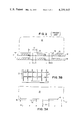
- FIG. 3B shows a section of the multi-aperture grid used by the present invention.
- FIG. 1 shows the reactive ion beam etching system in accordance with the present invention.
- a single grid ion source together with wafers and holders are contained within a vacuum chamber.
- the ion source includes a thermionic cathode 10 located within the chamber formed by the walls 12 of the ion source.
- a plurality of anodes 14 are disposed as shown around the ion source adjacent the walls 12 and are made of non-magnetic material such as stainless steel.
- the anodes 14 are located between pole pieces 16 on both sides of the anodes 14.
- the pole pieces 16 are made of a magnetically permeable material such as soft iron.
- a reactive gas such as CF 4 is provided into the ion source through a gas inlet 18.
- the gas is ionized by electrons from the cathode 10 which are accelerated to the anodes 14.
- Magnetic field lines 20 are produced between the pole pieces 16 and enhance the ionization efficiency.
- a multi-aperture accelerator grid 22 is shown at the lower end of the ion source, details of such grid 22 being described below.
- a plasma 24 is formed by the ions and electrons in the ion source chamber and provides a source of ions for the ion beam. These ions are extracted from the plasma 24 to the apertures in the accelerator grid 22 and form a beam shown by the ion trajectory lines 26 in the figure.
- Electrons are added to the beam 26 from a neutralizer 28 to prevent the charging up of insulating wafers 30.
- the wafers 30 to be patterned are bombarded with the low energy ion beam 26.
- Such wafers 30 are mounted on a wafer holder 32 and have masking material 34 on such wafers for delineating the desired patterns.
- Reactive species in the beam 26 combine with atoms in the wafer 30 to form etching products indicated by 35.
- etching products 35 are often volatile gases and will be removed by a pumping port 38 from the vacuum chamber indicated by 40.
- the masking material 34 is chosen so as not to react easily with the beam of ions 26, thereby remaining an effective mask while the wafers 30 are being patterned.
- FIG. 2 there is shown a dual grid ion milling system of the conventional type wherein a screen grid 42 is at a positive potential, close to the potential of the discharge-chamber plasma. Components not shown in FIG. 2 are similar to those shown in FIG. 1.
- the screen grid 42 serves to define the ion flow into small beamlets or ion trajectories 44 which are directed during normal operation to miss an accelerator grid 46.
- the plasma is indicated in FIG. 2 by 48 with each aperture indicated by 50.
- a plasma sheath 52 is formed adjacent the screen grid 42.
- the acceleration distance of the ions is indicated by 54 and represents the spacing between the accelerator grid 46 and the plasma 48 at the opposite side of the screen grid 42.
- the ion current density in the ion beam is limited by the acceleration distance 54 which cannot be made smaller than about 1-2 millimeters due to the presence of the screen grid 42.
- the accelerator grid 46 is negative relative to the neutralizer cathode, not shown, to prevent backstreaming of neutalizing electrons. Upon leaving the accelerator system, the beamlets from each aperture 50 coalesce to form a broad composite ion beam, not shown, further away from the apertures. The width of the apertures 50 in the grids is indicated by numeral 56.
- Additional grids are often used to improve focusing.
- An intermediate grid between the screen and accelerator grids has been used, as well as a grid grounded to the vacuum facility and neutralizer that is located on the neutralizer side of the accelerator grid.
- These additional grids do not ease the requirement for close grid spacings at high current densities.
- FIG. 3A there is shown the single grid reactive ion beam etching system described with respect to FIG. 1.
- the plasma 24, the accelerator grid 22 and the ion beam trajectories 26 are diagrammatically shown with the identical numerals as those shown and described with respect to FIG. 1.
- the acceleration distance is indicated by numeral 58 and is equal to the thickness of the plasma sheath adjacent the accelerator grid 22.
- This acceleration distance 58, or thickness of the sheath 60 increases with acceleration voltage, the potential difference between the plasma 24 and the accelerator grid 22. At low acceleration voltages this distance can approach the Debye length of the ions in the plasma, which is typically 0.1 mm.
- the single grid system shown in FIGS. 1 and 3 generates more ion current than the dual grid system according to the relationship of Child's law described above.
- the current density is inversely proportional to the square of the acceleration distance.
- the acceleration distance 58 shown in the single grid design of FIG. 3 is the sheath thickness which can be of the order of 0.1 millimeters, while the acceleration distance 54 in the dual-grid design of the prior art shown in FIG. 2 is in the order of 1-2 millimeters due to the presence of the screen grid 42 which places a limitation on the minimum size of the acceleration distance.
- V is the potential difference between the plasma 24 and the accelerator grid 22
- l is the acceleration distance 58. It is apparent that at low ion energy, the single grid system generates more ion current than the dual-grid system.
- FIG. 3B shows a portion of the acceleration grid 22 shown in FIG. 3A. It is noted that the acceleration distance 58 shown in FIG. 3A is larger than the size of the aperture 62 for the screen grid 22.
- the rectangular apertures 62 shown in the embodiment of FIG. 3A is one typical design, however, other shapes of apertures may be employed. In any event, for the screen grids employed in the subject system, the size of the aperture 62 must be about the acceleration distance or sheath thickness 58, or smaller.
- a single grid ion source was constructed to test the capability of etching semiconductor materials with reactive and inert gas ions.
- a nickel mesh grid was used with aperture size of 75 microns and wire size 10 microns.
- the ion beam diameter was 2.5 cm.
- argon or CF 4 (tetrafluoromethane) gas ion beams of 1 mA/cm 2 current density were obtained over the energy range of 20 to 100eV.
- wafers of Si and SiO 2 were exposed to ion beams of Ar on CF 4 of 100eV energy and etch rates were measured.
- the anodes 14 were held at a positive potential of 100V above ground.
- the single accelerator grid was held at a negative potential of -40V below ground.
- a discharge voltage of 40V was maintained between the cathode 10 and anodes 14 to maintain a discharge current of 0.1 amperes.
- a neutralizer filament 28 was heated by a current of 4 amperes to provide a flow of electrons to the substrate to balance the positive charge from the ion beam.
- a gas pressure of 2 ⁇ 10 31 4 Torr was maintained in the chamber 40.
- the wafers were located on a rotating water cooled holder 14 cm from the ion source. A mask was used to generate steps on the etched wafer surfaces which were then measured.
- SiO 2 etch rate 40A/min.
- Si etch rate 10A/min.
- SiO 2 etch rate ⁇ 0.1A/min.
- Si etch rate ⁇ 0.1A/min.
- etch rate ratio 4 to 1 between SiO 2 and Si was obtained. This etch rate ratio may be modified by changing the etching gas composition and ion energy.
- a directional ion beam may be aimed at the substrate at varying angles to produce either vertical etch walls or other wall profiles.
- the ion beam area can be increased to a large diameter of many cm. for large area processing.
- the acceleration distance must be maintained by mechanically holding the two grids at a predetermined required separation therebetween.
- the ion source is not only suitable as a research tool, but can be scaled up to production size.
- the subject invention provides a single grid accelerator system to produce a high current low energy ion beam for reactive sputtering and reactive ion etching. Also, high ion current densities are possible in large beam diameters because the acceleration distance is set by the plasma sheath rather than a mechanical spacing between grids.
Landscapes
- Chemical & Material Sciences (AREA)
- Analytical Chemistry (AREA)
- Engineering & Computer Science (AREA)
- Combustion & Propulsion (AREA)
- Physics & Mathematics (AREA)
- Plasma & Fusion (AREA)
- Drying Of Semiconductors (AREA)
Priority Applications (4)
| Application Number | Priority Date | Filing Date | Title |
|---|---|---|---|
| US06/053,491 US4259145A (en) | 1979-06-29 | 1979-06-29 | Ion source for reactive ion etching |
| JP4580980A JPS566441A (en) | 1979-06-29 | 1980-04-09 | Reactive ion beam etching method |
| EP80103077A EP0021140B1 (de) | 1979-06-29 | 1980-06-03 | Ionenquelle in einer Vakuumkammer und Verfahren zum Betrieb derselben |
| DE8080103077T DE3064623D1 (en) | 1979-06-29 | 1980-06-03 | Ion source in a vacuum chamber and method for its operation |
Applications Claiming Priority (1)
| Application Number | Priority Date | Filing Date | Title |
|---|---|---|---|
| US06/053,491 US4259145A (en) | 1979-06-29 | 1979-06-29 | Ion source for reactive ion etching |
Publications (1)
| Publication Number | Publication Date |
|---|---|
| US4259145A true US4259145A (en) | 1981-03-31 |
Family
ID=21984645
Family Applications (1)
| Application Number | Title | Priority Date | Filing Date |
|---|---|---|---|
| US06/053,491 Expired - Lifetime US4259145A (en) | 1979-06-29 | 1979-06-29 | Ion source for reactive ion etching |
Country Status (4)
| Country | Link |
|---|---|
| US (1) | US4259145A (2) |
| EP (1) | EP0021140B1 (2) |
| JP (1) | JPS566441A (2) |
| DE (1) | DE3064623D1 (2) |
Cited By (32)
| Publication number | Priority date | Publication date | Assignee | Title |
|---|---|---|---|---|
| US4351712A (en) * | 1980-12-10 | 1982-09-28 | International Business Machines Corporation | Low energy ion beam oxidation process |
| US4383177A (en) * | 1980-12-24 | 1983-05-10 | International Business Machines Corporation | Multipole implantation-isotope separation ion beam source |
| US4436581A (en) | 1981-04-22 | 1984-03-13 | Hitachi, Ltd. | Uniform etching of silicon (doped and undoped) utilizing ions |
| US4450031A (en) * | 1982-09-10 | 1984-05-22 | Nippon Telegraph & Telephone Public Corporation | Ion shower apparatus |
| FR2545984A1 (fr) * | 1983-05-11 | 1984-11-16 | Semiconductor Res Found | Procede de fabrication a sec d'un dispositif semi-conducteur par reaction photochimique et appareil pour la mise en oeuvre de ce procede |
| US4516050A (en) * | 1982-07-14 | 1985-05-07 | Varian Associates, Inc. | Ion chamber for electron-bombardment ion sources |
| US4522674A (en) * | 1983-01-24 | 1985-06-11 | Hitachi, Ltd. | Surface treatment apparatus |
| US4523971A (en) * | 1984-06-28 | 1985-06-18 | International Business Machines Corporation | Programmable ion beam patterning system |
| US4538067A (en) * | 1982-12-09 | 1985-08-27 | International Business Machines Corporation | Single grid focussed ion beam source |
| US4541890A (en) * | 1982-06-01 | 1985-09-17 | International Business Machines Corporation | Hall ion generator for working surfaces with a low energy high intensity ion beam |
| US4544444A (en) * | 1984-08-15 | 1985-10-01 | General Motors Corporation | Reactive ion etching of tin oxide films using silicon tetrachloride reactant gas |
| US4624214A (en) * | 1982-10-08 | 1986-11-25 | Hitachi, Ltd. | Dry-processing apparatus |
| US4778562A (en) * | 1984-08-13 | 1988-10-18 | General Motors Corporation | Reactive ion etching of tin oxide films using neutral reactant gas containing hydrogen |
| US4793961A (en) * | 1983-07-26 | 1988-12-27 | The United States Of America As Represented By The Department Of Energy | Method and source for producing a high concentration of positively charged molecular hydrogen or deuterium ions |
| US4931698A (en) * | 1988-04-12 | 1990-06-05 | Matsushita Electric Industrial Co., Ltd. | Ion source |
| US5580421A (en) * | 1994-06-14 | 1996-12-03 | Fsi International | Apparatus for surface conditioning |
| US5855745A (en) * | 1997-04-23 | 1999-01-05 | Sierra Applied Sciences, Inc. | Plasma processing system utilizing combined anode/ ion source |
| US5882538A (en) * | 1995-08-28 | 1999-03-16 | Georgia Tech Research Corporation | Method and apparatus for low energy electron enhanced etching of substrates |
| WO1999039860A1 (en) * | 1998-02-06 | 1999-08-12 | Plasmaquest, Inc. | Permanent magnet ecr plasma source with magnetic field optimization |
| US6015503A (en) * | 1994-06-14 | 2000-01-18 | Fsi International, Inc. | Method and apparatus for surface conditioning |
| US6027663A (en) * | 1995-08-28 | 2000-02-22 | Georgia Tech Research Corporation | Method and apparatus for low energy electron enhanced etching of substrates |
| US6033587A (en) * | 1996-09-20 | 2000-03-07 | Georgia Tech Research Corporation | Method and apparatus for low energy electron enhanced etching and cleaning of substrates in the positive column of a plasma |
| US6258287B1 (en) | 1996-08-28 | 2001-07-10 | Georgia Tech Research Corporation | Method and apparatus for low energy electron enhanced etching of substrates in an AC or DC plasma environment |
| US6663792B2 (en) | 1997-10-21 | 2003-12-16 | Fsi International, Inc. | Equipment for UV wafer heating and photochemistry |
| US20050020070A1 (en) * | 2001-09-28 | 2005-01-27 | Katsunori Ichiki | Etching method and apparatus |
| US20090189083A1 (en) * | 2008-01-25 | 2009-07-30 | Valery Godyak | Ion-beam source |
| US20110198314A1 (en) * | 2010-02-12 | 2011-08-18 | Headway Technologies, Inc. | Method to fabricate small dimension devices for magnetic recording applications |
| US20130327015A1 (en) * | 2012-06-12 | 2013-12-12 | Pamela Pollet | Dual use hydrazine propulsion thruster system |
| US8759223B2 (en) | 2011-08-26 | 2014-06-24 | Applied Materials, Inc. | Double patterning etching process |
| US20180166291A1 (en) * | 2013-10-14 | 2018-06-14 | Taiwan Semiconductor Manufacturing Company Ltd. | Semiconductor manufacturing apparatus and method thereof |
| WO2019126729A1 (en) * | 2017-12-22 | 2019-06-27 | Chirp Microsystems | Method for tuning a resonant frequency of a piezoelectric micromachined ultrasonic transducer |
| US10699876B2 (en) * | 2015-10-28 | 2020-06-30 | Advanced Ion Beam Technology, Inc. | Method of cleaning electrostatic chuck |
Families Citing this family (6)
| Publication number | Priority date | Publication date | Assignee | Title |
|---|---|---|---|---|
| DE3218728A1 (de) * | 1982-05-18 | 1984-03-01 | Telefunken electronic GmbH, 7100 Heilbronn | Ionenstrahl-aetzvorrichtung |
| US4690744A (en) * | 1983-07-20 | 1987-09-01 | Konishiroku Photo Industry Co., Ltd. | Method of ion beam generation and an apparatus based on such method |
| JPS6049629A (ja) * | 1983-08-29 | 1985-03-18 | Mitsubishi Electric Corp | 反応性イオンビ−ムエツチング装置 |
| JPS6355205A (ja) * | 1986-08-22 | 1988-03-09 | 福島 修 | 舗装面除去方法およびそれに用いる舗装切削装置 |
| SU1758086A1 (ru) * | 1990-06-26 | 1992-08-30 | Московский авиационный институт им.Серго Орджоникидзе | Устройство дл ионно-лучевой обработки деталей |
| EP0469236B1 (en) * | 1990-07-30 | 1995-09-20 | Hauzer Holding B.V. | Apparatus for ion-plasma machining workpiece surfaces |
Citations (8)
| Publication number | Priority date | Publication date | Assignee | Title |
|---|---|---|---|---|
| US3177654A (en) * | 1961-09-26 | 1965-04-13 | Ryan Aeronautical Company | Electric aerospace propulsion system |
| US3361659A (en) * | 1967-08-14 | 1968-01-02 | Ibm | Process of depositing thin films by cathode sputtering using a controlled grid |
| US3660715A (en) * | 1970-08-18 | 1972-05-02 | Atomic Energy Commission | Ion source with mosaic ion extraction means |
| US3969646A (en) * | 1975-02-10 | 1976-07-13 | Ion Tech, Inc. | Electron-bombardment ion source including segmented anode of electrically conductive, magnetic material |
| US4104086A (en) * | 1977-08-15 | 1978-08-01 | International Business Machines Corporation | Method for forming isolated regions of silicon utilizing reactive ion etching |
| US4119881A (en) * | 1978-02-27 | 1978-10-10 | Control Data Corporation | Ion beam generator having concentrically arranged frustoconical accelerating grids |
| US4139442A (en) * | 1977-09-13 | 1979-02-13 | International Business Machines Corporation | Reactive ion etching method for producing deep dielectric isolation in silicon |
| US4158589A (en) * | 1977-12-30 | 1979-06-19 | International Business Machines Corporation | Negative ion extractor for a plasma etching apparatus |
Family Cites Families (10)
| Publication number | Priority date | Publication date | Assignee | Title |
|---|---|---|---|---|
| US3156090A (en) * | 1961-09-18 | 1964-11-10 | Harold R Kaufman | Ion rocket |
| FR1402020A (fr) * | 1964-04-27 | 1965-06-11 | Csf | Perfectionnements aux sources d'ions |
| DE1565173A1 (de) * | 1965-04-02 | 1970-03-19 | Halbleiterwerk Frankfurt Oder | Verfahren und Vorrichtung zur Behandlung von elektrisch leitendem Material,insbesondere Halbleitermaterial |
| JPS4948119B1 (2) * | 1969-12-19 | 1974-12-19 | ||
| FR2096876B1 (2) * | 1970-07-09 | 1973-08-10 | Thomson Csf | |
| US3744247A (en) * | 1971-09-14 | 1973-07-10 | Nasa | Single grid accelerator for an ion thrustor |
| FR2218652B1 (2) * | 1973-02-20 | 1976-09-10 | Thomson Csf | |
| US3908183A (en) * | 1973-03-14 | 1975-09-23 | California Linear Circuits Inc | Combined ion implantation and kinetic transport deposition process |
| DE2536718C3 (de) * | 1975-08-18 | 1978-04-27 | Siemens Ag, 1000 Berlin Und 8000 Muenchen | Verfahren zur Herstellung geätzter Strukturen in Festkörperoberflächen durch Ionenätzung und Bestrahlungsmaske zur Verwendung in diesem Verfahren |
| DE2625870A1 (de) * | 1976-06-09 | 1977-12-22 | Siemens Ag | Fotolithografisches aetzverfahren |
-
1979
- 1979-06-29 US US06/053,491 patent/US4259145A/en not_active Expired - Lifetime
-
1980
- 1980-04-09 JP JP4580980A patent/JPS566441A/ja active Granted
- 1980-06-03 EP EP80103077A patent/EP0021140B1/de not_active Expired
- 1980-06-03 DE DE8080103077T patent/DE3064623D1/de not_active Expired
Patent Citations (8)
| Publication number | Priority date | Publication date | Assignee | Title |
|---|---|---|---|---|
| US3177654A (en) * | 1961-09-26 | 1965-04-13 | Ryan Aeronautical Company | Electric aerospace propulsion system |
| US3361659A (en) * | 1967-08-14 | 1968-01-02 | Ibm | Process of depositing thin films by cathode sputtering using a controlled grid |
| US3660715A (en) * | 1970-08-18 | 1972-05-02 | Atomic Energy Commission | Ion source with mosaic ion extraction means |
| US3969646A (en) * | 1975-02-10 | 1976-07-13 | Ion Tech, Inc. | Electron-bombardment ion source including segmented anode of electrically conductive, magnetic material |
| US4104086A (en) * | 1977-08-15 | 1978-08-01 | International Business Machines Corporation | Method for forming isolated regions of silicon utilizing reactive ion etching |
| US4139442A (en) * | 1977-09-13 | 1979-02-13 | International Business Machines Corporation | Reactive ion etching method for producing deep dielectric isolation in silicon |
| US4158589A (en) * | 1977-12-30 | 1979-06-19 | International Business Machines Corporation | Negative ion extractor for a plasma etching apparatus |
| US4119881A (en) * | 1978-02-27 | 1978-10-10 | Control Data Corporation | Ion beam generator having concentrically arranged frustoconical accelerating grids |
Non-Patent Citations (1)
| Title |
|---|
| Vossen et al., ed. Thin Film Processes, Academic Press, New York, N.Y., (1978), pp. 497-553. * |
Cited By (47)
| Publication number | Priority date | Publication date | Assignee | Title |
|---|---|---|---|---|
| US4351712A (en) * | 1980-12-10 | 1982-09-28 | International Business Machines Corporation | Low energy ion beam oxidation process |
| US4383177A (en) * | 1980-12-24 | 1983-05-10 | International Business Machines Corporation | Multipole implantation-isotope separation ion beam source |
| US4436581A (en) | 1981-04-22 | 1984-03-13 | Hitachi, Ltd. | Uniform etching of silicon (doped and undoped) utilizing ions |
| US4541890A (en) * | 1982-06-01 | 1985-09-17 | International Business Machines Corporation | Hall ion generator for working surfaces with a low energy high intensity ion beam |
| US4516050A (en) * | 1982-07-14 | 1985-05-07 | Varian Associates, Inc. | Ion chamber for electron-bombardment ion sources |
| US4450031A (en) * | 1982-09-10 | 1984-05-22 | Nippon Telegraph & Telephone Public Corporation | Ion shower apparatus |
| US4624214A (en) * | 1982-10-08 | 1986-11-25 | Hitachi, Ltd. | Dry-processing apparatus |
| US4538067A (en) * | 1982-12-09 | 1985-08-27 | International Business Machines Corporation | Single grid focussed ion beam source |
| US4522674A (en) * | 1983-01-24 | 1985-06-11 | Hitachi, Ltd. | Surface treatment apparatus |
| FR2545984A1 (fr) * | 1983-05-11 | 1984-11-16 | Semiconductor Res Found | Procede de fabrication a sec d'un dispositif semi-conducteur par reaction photochimique et appareil pour la mise en oeuvre de ce procede |
| US4540466A (en) * | 1983-05-11 | 1985-09-10 | Semiconductor Research Foundation | Method of fabricating semiconductor device by dry process utilizing photochemical reaction, and apparatus therefor |
| US4793961A (en) * | 1983-07-26 | 1988-12-27 | The United States Of America As Represented By The Department Of Energy | Method and source for producing a high concentration of positively charged molecular hydrogen or deuterium ions |
| US4523971A (en) * | 1984-06-28 | 1985-06-18 | International Business Machines Corporation | Programmable ion beam patterning system |
| US4778562A (en) * | 1984-08-13 | 1988-10-18 | General Motors Corporation | Reactive ion etching of tin oxide films using neutral reactant gas containing hydrogen |
| US4544444A (en) * | 1984-08-15 | 1985-10-01 | General Motors Corporation | Reactive ion etching of tin oxide films using silicon tetrachloride reactant gas |
| US4931698A (en) * | 1988-04-12 | 1990-06-05 | Matsushita Electric Industrial Co., Ltd. | Ion source |
| US6015503A (en) * | 1994-06-14 | 2000-01-18 | Fsi International, Inc. | Method and apparatus for surface conditioning |
| US5580421A (en) * | 1994-06-14 | 1996-12-03 | Fsi International | Apparatus for surface conditioning |
| US6027663A (en) * | 1995-08-28 | 2000-02-22 | Georgia Tech Research Corporation | Method and apparatus for low energy electron enhanced etching of substrates |
| US5882538A (en) * | 1995-08-28 | 1999-03-16 | Georgia Tech Research Corporation | Method and apparatus for low energy electron enhanced etching of substrates |
| US6852195B2 (en) | 1996-08-28 | 2005-02-08 | Georgia Tech Research Corporation | Method and apparatus for low energy electron enhanced etching of substrates in an AC or DC plasma environment |
| US7431796B2 (en) | 1996-08-28 | 2008-10-07 | Georgia Tech Research Corporation | Method and apparatus for low energy electron enhanced etching of substrates in an AC or DC plasma environment |
| US6258287B1 (en) | 1996-08-28 | 2001-07-10 | Georgia Tech Research Corporation | Method and apparatus for low energy electron enhanced etching of substrates in an AC or DC plasma environment |
| WO2000033362A1 (en) * | 1996-08-28 | 2000-06-08 | Georgia Tech Research Corporation | Method and apparatus for low energy electron enhanced etching of substrates |
| US20040163763A1 (en) * | 1996-08-28 | 2004-08-26 | Martin Kevin P. | Method and apparatus for low energy electron enhanced etching of substrates in an AC or DC plasma environment |
| US6033587A (en) * | 1996-09-20 | 2000-03-07 | Georgia Tech Research Corporation | Method and apparatus for low energy electron enhanced etching and cleaning of substrates in the positive column of a plasma |
| US5855745A (en) * | 1997-04-23 | 1999-01-05 | Sierra Applied Sciences, Inc. | Plasma processing system utilizing combined anode/ ion source |
| US6663792B2 (en) | 1997-10-21 | 2003-12-16 | Fsi International, Inc. | Equipment for UV wafer heating and photochemistry |
| WO2000032851A1 (en) * | 1997-12-03 | 2000-06-08 | Georgia Tech Research Corporation | Method and apparatus for low energy electron enhanced etching and cleaning of substrates |
| WO1999039860A1 (en) * | 1998-02-06 | 1999-08-12 | Plasmaquest, Inc. | Permanent magnet ecr plasma source with magnetic field optimization |
| US6163006A (en) * | 1998-02-06 | 2000-12-19 | Astex-Plasmaquest, Inc. | Permanent magnet ECR plasma source with magnetic field optimization |
| US20050020070A1 (en) * | 2001-09-28 | 2005-01-27 | Katsunori Ichiki | Etching method and apparatus |
| US7314574B2 (en) * | 2001-09-28 | 2008-01-01 | Ebara Corporation | Etching method and apparatus |
| US20090189083A1 (en) * | 2008-01-25 | 2009-07-30 | Valery Godyak | Ion-beam source |
| US7863582B2 (en) | 2008-01-25 | 2011-01-04 | Valery Godyak | Ion-beam source |
| US20110198314A1 (en) * | 2010-02-12 | 2011-08-18 | Headway Technologies, Inc. | Method to fabricate small dimension devices for magnetic recording applications |
| US8728333B2 (en) * | 2010-02-12 | 2014-05-20 | Headway Technologies, Inc. | Method to fabricate small dimension devices for magnetic recording applications |
| US8759223B2 (en) | 2011-08-26 | 2014-06-24 | Applied Materials, Inc. | Double patterning etching process |
| US20130327015A1 (en) * | 2012-06-12 | 2013-12-12 | Pamela Pollet | Dual use hydrazine propulsion thruster system |
| US20180166291A1 (en) * | 2013-10-14 | 2018-06-14 | Taiwan Semiconductor Manufacturing Company Ltd. | Semiconductor manufacturing apparatus and method thereof |
| US10763117B2 (en) * | 2013-10-14 | 2020-09-01 | Taiwan Semiconductor Manufacturing Company Ltd. | Semiconductor manufacturing apparatus and method thereof |
| US20220367197A1 (en) * | 2013-10-14 | 2022-11-17 | Taiwan Semiconductor Manufacturing Company Ltd. | Method for manufacturing semiconductor structure |
| US11908700B2 (en) * | 2013-10-14 | 2024-02-20 | Taiwan Semiconductor Manufacturing Company Ltd. | Method for manufacturing semiconductor structure |
| US10699876B2 (en) * | 2015-10-28 | 2020-06-30 | Advanced Ion Beam Technology, Inc. | Method of cleaning electrostatic chuck |
| WO2019126729A1 (en) * | 2017-12-22 | 2019-06-27 | Chirp Microsystems | Method for tuning a resonant frequency of a piezoelectric micromachined ultrasonic transducer |
| US11938515B2 (en) | 2017-12-22 | 2024-03-26 | Invensense, Inc. | Method for tuning the resonant frequency of a piezoelectric micromachined ultrasonic transducer |
| US12226801B2 (en) | 2017-12-22 | 2025-02-18 | Invensense, Inc. | Apparatus and system for tuning the resonant frequency of a piezoelectric micromachined ultrasonic transducer |
Also Published As
| Publication number | Publication date |
|---|---|
| EP0021140A1 (de) | 1981-01-07 |
| JPS566441A (en) | 1981-01-23 |
| JPS5719570B2 (2) | 1982-04-23 |
| EP0021140B1 (de) | 1983-08-24 |
| DE3064623D1 (en) | 1983-09-29 |
Similar Documents
| Publication | Publication Date | Title |
|---|---|---|
| US4259145A (en) | Ion source for reactive ion etching | |
| US4521286A (en) | Hollow cathode sputter etcher | |
| US4351712A (en) | Low energy ion beam oxidation process | |
| US5022977A (en) | Ion generation apparatus and thin film forming apparatus and ion source utilizing the ion generation apparatus | |
| EP0328076B1 (en) | Thin film forming apparatus and ion source utilizing sputtering with microwave plasma | |
| US4277304A (en) | Ion source and ion etching process | |
| US5156703A (en) | Mthod for the surface treatment of semiconductors by particle bombardment | |
| US4422896A (en) | Magnetically enhanced plasma process and apparatus | |
| US4581118A (en) | Shaped field magnetron electrode | |
| US5135634A (en) | Apparatus for depositing a thin layer of sputtered atoms on a member | |
| US4541890A (en) | Hall ion generator for working surfaces with a low energy high intensity ion beam | |
| JP2001520433A (ja) | 加速された粒子を発生させる装置並びに方法 | |
| US4414069A (en) | Negative ion beam selective etching process | |
| Ishikawa et al. | Mass‐separated negative‐ion‐beam deposition system | |
| US4496449A (en) | Electron beam etching of integrated circuit structures | |
| US4749910A (en) | Electron beam-excited ion beam source | |
| US7510666B2 (en) | Time continuous ion-ion plasma | |
| Horwitz | Hollow cathode reactive sputter etching—A new high‐rate process | |
| Matsuo et al. | Gas cluster ion beam equipments for industrial applications | |
| US5728261A (en) | Magnetically enhanced radio frequency reactive ion etching method and apparatus | |
| Ryu et al. | Trajectories of ions inside a Faraday cage located in a high density plasma etcher | |
| Kaufman et al. | Broad-beam ion source technology and applications | |
| JPH05102083A (ja) | ドライエツチング方法及びそのための装置 | |
| US5853521A (en) | Multi-cathode electron beam plasma etcher | |
| US7911120B2 (en) | Source for providing an electron beam of settable power |