US4260935A - Circuit arrangement for suppressing CRT beam in television receiver - Google Patents
Circuit arrangement for suppressing CRT beam in television receiver Download PDFInfo
- Publication number
- US4260935A US4260935A US06/073,088 US7308879A US4260935A US 4260935 A US4260935 A US 4260935A US 7308879 A US7308879 A US 7308879A US 4260935 A US4260935 A US 4260935A
- Authority
- US
- United States
- Prior art keywords
- transistor
- signal
- pulse
- input
- slave
- Prior art date
- Legal status (The legal status is an assumption and is not a legal conclusion. Google has not performed a legal analysis and makes no representation as to the accuracy of the status listed.)
- Expired - Lifetime
Links
- 230000000737 periodic effect Effects 0.000 claims abstract 2
- 230000003213 activating effect Effects 0.000 claims description 6
- 230000008034 disappearance Effects 0.000 claims description 2
- 229920006395 saturated elastomer Polymers 0.000 abstract description 3
- 230000001629 suppression Effects 0.000 abstract description 3
- 239000003990 capacitor Substances 0.000 description 8
- 238000010586 diagram Methods 0.000 description 3
- 239000013256 coordination polymer Substances 0.000 description 2
- 230000007257 malfunction Effects 0.000 description 2
- 230000001681 protective effect Effects 0.000 description 2
- 230000000306 recurrent effect Effects 0.000 description 2
- 238000009738 saturating Methods 0.000 description 2
- 230000002159 abnormal effect Effects 0.000 description 1
Images

Classifications
-
- H—ELECTRICITY
- H04—ELECTRIC COMMUNICATION TECHNIQUE
- H04N—PICTORIAL COMMUNICATION, e.g. TELEVISION
- H04N3/00—Scanning details of television systems; Combination thereof with generation of supply voltages
- H04N3/10—Scanning details of television systems; Combination thereof with generation of supply voltages by means not exclusively optical-mechanical
- H04N3/16—Scanning details of television systems; Combination thereof with generation of supply voltages by means not exclusively optical-mechanical by deflecting electron beam in cathode-ray tube, e.g. scanning corrections
- H04N3/20—Prevention of damage to cathode-ray tubes in the event of failure of scanning
Definitions
- My present invention relates to a circuit arrangement for the suppression of the beam of a cathode-ray tube in a televisions receiver during flyback as well as in the event of a malfunction.
- Conventional sweep circuits used for horizontal and vertical scanning in television receivers periodically emit a blanking pulse, derived from the sawtooth voltage of a respective ramp generator, in order to suppress the beam during its return stroke.
- Such a system generally comprises a storage capacitor chargeable by a guard circuit in response to the flyback pulse; in the discharged state of the capacitor, the blanking pulse is extended into a continuous d-c voltage whereby the beam is permanently cut off. See, for example, Technical Note 078 by N. V. Philips'Gloeilampenfabrieken (1978) relating to the integrated vertical-deflection module known as TDA2652.
- the storage capacitor used with such a prior-art guard circuit must be fairly large, with a capacitance of at least one microfarad. Such capacitors cannot be incorporated in an integrated-circuit module and are therefore designed as separate circuit components connected to the i-c chip via an external terminal.
- the general object of my present invention is to provide a circuit arrangement of the type referred to which obviates the need for a separate capacitor designed to store the flyback pulse.
- a related object is to provide a more compact unit of this description which is realizable entirely by integrated circuitry.
- I provide a normally deactivated comparator with a first signal input for receiving a switching signal from a first biasing circuit and a second signal input for receiving a reference signal from a second biasing circuit.
- a control circuit with an output connection extending to an activating input of the comparator receives the blanking pulse from the sweep circuit via an input connection and a holding signal from the comparator via a feedback connection whenever that comparator is activated in response to such a blanking pulse to assume a first operational state; the holding signal then maintains that operational state independently of the blanking pulse.
- This first biasing circuit is coupled to switchover means such as a shunt transistor connected to receive the flyback pulse and, in response to that pulse, modifies the switching signal emitted by it to establish a second operational state of the comparator with concurrent disablement of the feedback connection to the control circuit.
- switchover means such as a shunt transistor connected to receive the flyback pulse and, in response to that pulse, modifies the switching signal emitted by it to establish a second operational state of the comparator with concurrent disablement of the feedback connection to the control circuit.
- the output connection of the control circuit includes a master transistor and several slave or follower transistors which are interconnected in a current-mirror configuration, one such slave transistor being connected to the activating input of the comparator for energizing same upon conduction of the associated master transistor.
- Another slave transistor so associated may form part of the first biasing circuit and of the output circuit which generates the beam-suppressing signal.
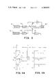
- FIG. 1 is a block diagram of a conventional guard circuit for suppressing the beam of a CRT tube
- FIG. 2 is a circuit diagram of a protective arrangement embodying my invention, having the same purpose as the device of FIG. 1 but consisting only of resistors and electronic switches realizable by integrated circuitry;
- FIG. 3 is a generalized representation, in block form, of the circuitry shown in FIG. 2;
- FIGS. 4a and 4b are two sets of graphs depicting the mode of operation of the system of FIG. 2 under normal and under abnormal circumstances, respectively.
- FIG. 1 I have shown a conventional beam suppressor, such as the above-mentioned guard circuit of the TDA2652 modlule, receiving a recurrent blanking pulse V b1 of negativve polarity from a generator G b1 and an accompanying flyback pulse V fb of positive polarity, of shorter duration, form another generator G fb .
- the flyback pulse V fb is applied to the base of a PNP transistor T 1 connected in cascade with two similar transistors T 2 and T 3 ; all three transistors have their collector/emitter paths connected in parallel, through respective series resistors, across a source of d-c voltage +V.
- An R/C network in the input of transistor T 1 includes a storage capacitor CP which is charged by recurrent flyback pulses V fb so as to saturate the transistor T 1 whereby transistor T 2 is cut off and transistor T 3 conducts, except in the presence of a blanking pulse V b1 applied to its base to override the voltage +V on the collector of transistor T 2 whereby a positive beam-suppressing pulse V 3 appears on the collector of transistor T 3 .
- Generator G b1 is driven by a nonillustrated sawtooth oscillator included in the vertical-sweep circuit associated with the cathode-ray tube of a television receiver whose beam is to be cut off during flyback and in the event of a malfunction of that sweep circuit, as discussed above.
- G fb may comprise a small capacitor connected across the vertical-deflection yoke of that cathode-ray tube, as in the aforedescribed TDA2652 module.
- Capacitor CP as noted above, constitutes an extraneous component of the guard circuit represented by transistors T 1 -T 3 .
- FIG. 2 I have shown a pair of generators G 1 and G 2 which are similar to components G b1 and G fb of FIG. 1 but produce a flyback pulse V 1 and a blanking pulse V 2 both of positive polarity. These two pulses have also been illustrated in the timing diagrams of FIGS. 4a and 4b which indicate that the blanking pulse V 2 lasts for a longer period t 1 -t 4 than the accompanying flyback pulse V 1 occurring between times t 2 and t 3 ; the two pulse widths may be 1.2 msec. and 0.5 msec., respectively.
- the illustrated offset t 1 -t 2 between the leading edges of pulses V 2 and V 1 is not essential for the operation of the system but will generally occur in practice.
- the integrated circuitry shown in FIG. 2, serving to derive beam-suppressing signals from flyback and blanking pulses V 1 and V 2 may be conceptually subdivided into five components also illustrated in block form in FIG. 3, namely a comparator CMP, first and second biasing circuits PL1, PL2, a control circuit COM and an output circuit or final stage SF, all inserted between ground and a positive supply terminal +V.
- Components COM and PL1 share common circuit elements and have therefore not been separately indicated in FIG. 2.
- p Comparator CMP has two signal inputs A and B represented by the bases of respective PNP transistors T 4 and T 5 whose emitters are connected in parallel to the collector of a similar transistor T 6 and whose collectors are grounded via respective series resistors R 1 and R 2 .
- PNP transistor T 6 is one of four such transistors with emitters joined to supply terminal +V and with bases interconnected by a lead Y in a current-mirror configuration; the remaining transistors of this configuration have been designated T 7 , T 8 and T 13 , with transistor T 7 acting as the master and the others serving as followers.
- the collector of master transistor T 7 tied to lead Y, is connected by way of a voltage divider R 4 , R 8 to the emitters of two NPN transistors T 11 , T 12 inserted in parallel between that voltage divider and ground, these latter transistors forming part of control circuit COM.
- a shunt transistor T 9 also of NPN type, has its collector tied to the junction of resistors R 4 , R 8 and its emitter grounded. Transistor T 9 , whose base receives the flyback pulse V 1 from generator G 1 , conducts only in the presenc of that pulse to switch over the comparator CMP from a first to a second operational state as described hereinafter.
- Slave transistor T 8 has its collector connected to the base of transistor T 4 at comparator input A from which a biasing resistor R 3 extends to ground.
- the opposite input B i.e. the base of transistor T 5 , is connected to the junction of two series resistors R 5 and R 6 forming with a further series resistor R 7 a voltage divider inserted between terminal +V and ground.
- This voltage divider is part of biasing circuit PL2, as is an NPN transistor T 10 which constitutes an electronic bypass switch connected across resistor R 7 .
- the collectors of the two symmetrical comparator transistors T 4 and T 5 are respectively joined to the base of transistor T 12 via a lead C and to the base of transistor T 10 via a lead D; lead C constitutes a feedback connection delivering a holding signal to control circuit COM as will also be described hereinafter.
- Slave transistor T 13 is part of output circuit SF and has its collector grounded through a resistor R 9 in parallel with a Zener diode DZ.
- the output terminal 0 of the system, producing the beam-suppressing signal, lies at the junction of the collector of transistor T 13 with impedance network R 9 , DZ.
- transistors T 11 , T 12 of control circuit COM are cut off whereby master transistor T 7 and the associated slave transistors T 6 , T 8 and T 13 are likewise nonconducting.
- the potential of comparator input A shown at V A in FIG. 4a, is then at ground level and well below the magnitude of the reference signal V B applied to the other input B by biasing circuit PL2.
- Neither of transistors T 4 and T 5 conducts at this stage, however, in view of the cutoff of transistor T 6 .
- Shunt transistor T 9 and bypass transistor T 10 are also nonconducting; the voltage of output terminal 0 is likewise at ground level as seen at V o in FIG. 4a.
- flyback pulse V 1 effectively reinserts the resistor R 8 in the collector lead of master transistor T 7 , thereby raising once more the potential of lead Y so that the switching voltage at point A is again lowered to its previous level V A '. Since, however, point B is still more negative than point A, the state of comparator CMP does not change until instant t 4 when the trailing edge of blanking pulse V 2 restores the original condition of the system.
- comparator CMP would have remained in its first operational state with voltages of points A and B at their respective levels V A ' and V B , as shown in FIG. 4b.
- the output signal on terminal 0 would therefore have remained at its high level V z instead of returning to ground potential V o as in FIG. 4a, thereby continuing the suppression of the beam of the associated cathode-ray tube.
- comparator CMP is shown to have two separate output leads C and D respectively extending to control circuit COM and biasing circuit PL2, it will be apparent that these two leads could be replaced by a single output connection with two branches, one of them including an inverter INV, as illustrated in FIG. 3.
Landscapes
- Engineering & Computer Science (AREA)
- Multimedia (AREA)
- Signal Processing (AREA)
- Details Of Television Scanning (AREA)
- Transforming Electric Information Into Light Information (AREA)
- Electronic Switches (AREA)
Applications Claiming Priority (2)
| Application Number | Priority Date | Filing Date | Title |
|---|---|---|---|
| IT27399A/78 | 1978-09-07 | ||
| IT27399/78A IT1098809B (it) | 1978-09-07 | 1978-09-07 | Circuito per il comando dello spegnimento del fascio elettronico di un cinescopio |
Publications (1)
| Publication Number | Publication Date |
|---|---|
| US4260935A true US4260935A (en) | 1981-04-07 |
Family
ID=11221571
Family Applications (1)
| Application Number | Title | Priority Date | Filing Date |
|---|---|---|---|
| US06/073,088 Expired - Lifetime US4260935A (en) | 1978-09-07 | 1979-09-06 | Circuit arrangement for suppressing CRT beam in television receiver |
Country Status (7)
| Country | Link |
|---|---|
| US (1) | US4260935A (it) |
| JP (1) | JPS5555671A (it) |
| DE (1) | DE2934338A1 (it) |
| FR (1) | FR2435873A1 (it) |
| GB (1) | GB2032739B (it) |
| IT (1) | IT1098809B (it) |
| SE (1) | SE438400B (it) |
Cited By (2)
| Publication number | Priority date | Publication date | Assignee | Title |
|---|---|---|---|---|
| US5300865A (en) * | 1990-02-10 | 1994-04-05 | Deutsche Thomson-Brandt Gmbh | Self adjusting blanking signal generator |
| CN104393855B (zh) * | 2014-10-31 | 2017-04-19 | 广西师范学院 | 一种三稳态触发器 |
Families Citing this family (1)
| Publication number | Priority date | Publication date | Assignee | Title |
|---|---|---|---|---|
| GB2160078A (en) * | 1984-06-05 | 1985-12-11 | Motorola Inc | Failure detection circuit |
Citations (1)
| Publication number | Priority date | Publication date | Assignee | Title |
|---|---|---|---|---|
| US4176301A (en) * | 1977-03-17 | 1979-11-27 | U.S. Philips Corporation | Circuit arrangement for supplying a protection signal for a television picture display tube |
Family Cites Families (1)
| Publication number | Priority date | Publication date | Assignee | Title |
|---|---|---|---|---|
| US3763315A (en) * | 1971-07-22 | 1973-10-02 | Rca Corp | Blanking circuits for television receivers |
-
1978
- 1978-09-07 IT IT27399/78A patent/IT1098809B/it active
-
1979
- 1979-08-23 SE SE7907048A patent/SE438400B/sv not_active IP Right Cessation
- 1979-08-24 DE DE19792934338 patent/DE2934338A1/de not_active Withdrawn
- 1979-08-31 GB GB7930204A patent/GB2032739B/en not_active Expired
- 1979-09-06 FR FR7922302A patent/FR2435873A1/fr active Granted
- 1979-09-06 JP JP11363579A patent/JPS5555671A/ja active Pending
- 1979-09-06 US US06/073,088 patent/US4260935A/en not_active Expired - Lifetime
Patent Citations (1)
| Publication number | Priority date | Publication date | Assignee | Title |
|---|---|---|---|---|
| US4176301A (en) * | 1977-03-17 | 1979-11-27 | U.S. Philips Corporation | Circuit arrangement for supplying a protection signal for a television picture display tube |
Non-Patent Citations (1)
| Title |
|---|
| Philips, Technical Note 078, TDA2652-Integrated Vertical Deflection for 30AX. * |
Cited By (2)
| Publication number | Priority date | Publication date | Assignee | Title |
|---|---|---|---|---|
| US5300865A (en) * | 1990-02-10 | 1994-04-05 | Deutsche Thomson-Brandt Gmbh | Self adjusting blanking signal generator |
| CN104393855B (zh) * | 2014-10-31 | 2017-04-19 | 广西师范学院 | 一种三稳态触发器 |
Also Published As
| Publication number | Publication date |
|---|---|
| IT1098809B (it) | 1985-09-18 |
| JPS5555671A (en) | 1980-04-23 |
| GB2032739A (en) | 1980-05-08 |
| GB2032739B (en) | 1982-12-15 |
| SE7907048L (sv) | 1980-03-08 |
| DE2934338A1 (de) | 1980-03-27 |
| FR2435873B1 (it) | 1983-07-01 |
| IT7827399A0 (it) | 1978-09-07 |
| FR2435873A1 (fr) | 1980-04-04 |
| SE438400B (sv) | 1985-04-15 |
Similar Documents
| Publication | Publication Date | Title |
|---|---|---|
| US4045742A (en) | High voltage shutdown circuit responsive to excessive beam current and high voltage | |
| US4090111A (en) | Malfunction detecting apparatus for use in a CRT deflection circuit | |
| US4056758A (en) | Light spot suppression circuit for a cathode ray tube | |
| CA2041228C (en) | Protection circuit for a cathode ray tube | |
| JPS6239591B2 (it) | ||
| US4260935A (en) | Circuit arrangement for suppressing CRT beam in television receiver | |
| US3885201A (en) | Fail-safe high voltage protection circuit | |
| US4182992A (en) | Pulse width modulated signal amplifier | |
| US5084657A (en) | Spot killer circuit having blanking function | |
| US3863106A (en) | Vertical deflection circuit | |
| US3215948A (en) | Triggering circuit for automatically changing the mode of operation of a signal generator | |
| US4233635A (en) | High voltage limiting circuit for a television receiver | |
| US3819955A (en) | Counter circuit using current source | |
| US4169241A (en) | Overvoltage protected de-boost regulator | |
| US4042859A (en) | Horizontal deflection circuit of a television receiver with means to eliminate generation of dangerous high potential under faulty condition | |
| US3411032A (en) | Transistor television deflection circuits having protection means | |
| US3898525A (en) | Hysteresis voltage supply for deflection synchronizing waveform generator | |
| GB2077544A (en) | Drive circuits for a high resolution cathode ray tube display | |
| US3525011A (en) | Circuit arrangement for controlling the beam of a cathode-ray tube | |
| KR950009652B1 (ko) | 편향회로 | |
| US4353013A (en) | Drive circuits for a high resolutions cathode ray tube display | |
| US4164687A (en) | Television kinescope protection circuit | |
| US3794877A (en) | Jitter immune transistorized vertical deflection circuit | |
| US3449622A (en) | Television deflection circuits | |
| JPH01268355A (ja) | テレビジョン偏向装置 |