US4549280A - Apparatus for creating a multiplication pipeline of arbitrary size - Google Patents
Apparatus for creating a multiplication pipeline of arbitrary size Download PDFInfo
- Publication number
- US4549280A US4549280A US06/451,130 US45113082A US4549280A US 4549280 A US4549280 A US 4549280A US 45113082 A US45113082 A US 45113082A US 4549280 A US4549280 A US 4549280A
- Authority
- US
- United States
- Prior art keywords
- parity
- bit
- multiply
- multiplier
- carry
- Prior art date
- Legal status (The legal status is an assumption and is not a legal conclusion. Google has not performed a legal analysis and makes no representation as to the accuracy of the status listed.)
- Expired - Lifetime
Links
Images
Classifications
-
- G—PHYSICS
- G06—COMPUTING OR CALCULATING; COUNTING
- G06F—ELECTRIC DIGITAL DATA PROCESSING
- G06F7/00—Methods or arrangements for processing data by operating upon the order or content of the data handled
- G06F7/38—Methods or arrangements for performing computations using exclusively denominational number representation, e.g. using binary, ternary, decimal representation
- G06F7/48—Methods or arrangements for performing computations using exclusively denominational number representation, e.g. using binary, ternary, decimal representation using non-contact-making devices, e.g. tube, solid state device; using unspecified devices
- G06F7/52—Multiplying; Dividing
- G06F7/523—Multiplying only
- G06F7/53—Multiplying only in parallel-parallel fashion, i.e. both operands being entered in parallel
- G06F7/5324—Multiplying only in parallel-parallel fashion, i.e. both operands being entered in parallel partitioned, i.e. using repetitively a smaller parallel parallel multiplier or using an array of such smaller multipliers
-
- G—PHYSICS
- G06—COMPUTING OR CALCULATING; COUNTING
- G06F—ELECTRIC DIGITAL DATA PROCESSING
- G06F11/00—Error detection; Error correction; Monitoring
- G06F11/07—Responding to the occurrence of a fault, e.g. fault tolerance
- G06F11/08—Error detection or correction by redundancy in data representation, e.g. by using checking codes
- G06F11/10—Adding special bits or symbols to the coded information, e.g. parity check, casting out 9's or 11's
-
- G—PHYSICS
- G06—COMPUTING OR CALCULATING; COUNTING
- G06F—ELECTRIC DIGITAL DATA PROCESSING
- G06F2207/00—Indexing scheme relating to methods or arrangements for processing data by operating upon the order or content of the data handled
- G06F2207/38—Indexing scheme relating to groups G06F7/38 - G06F7/575
- G06F2207/3804—Details
- G06F2207/386—Special constructional features
- G06F2207/3884—Pipelining
Definitions
- This invention relates to a multibit multiplier which increases performance for the multiply operations of a large scale processor by providing a building block which may be used in a multiplication pipeline of arbitrary size.
- Such arrays are commonly built of a combination of adders and multiplexers, with multiplier decoders used for control.
- the adders used may be of the conventional type or they may take the carry/save form.
- Multiplication of binary fractions is normally implemented as the addition of a number of summands, each some simple multiple of the multiplicand, chosen from a limited set of available multiples on the basis of one or more multiplier digits. No good reason is known to depart from this general scheme. Acceleration of the process must then be based on one or more of the following expedients: (1) reduction in the number of summands; (2) acceleration of the formation of summands; (3) acceleration of the addition of summands. Acceleration of addition will be discussed initially.
- a simple form for such an adder is a string of full adder circuits of the normal sort, where the carry inputs are used for the third input number, and the carry outputs for the second output number.
- one pseudoadder is usually used, and storage is provided for two numbers. On each pass through the adder, the two stored numbers and one multiple of the multiplicand are added, and the resulting two numbers returned to storage.
- the number of adder passes occurring in a multiplication before the product is reduced to the sum of two numbers will be two less than the number of summands, since each pass through an adder converts three numbers of two, reducing the count of numbers by one.
- one must arrange many of these passes to occur simultaneously by providing several pseudoadders.
- the best possible first step is to group the summands into threes, and introduce each group into its own pseudoadder, thus reducing the count of numbers by a factor of 1.5 (or a little less, if the number of summands is not a multiple of three).
- the best possible second step is to group the numbers resulting from the first step into threes and again add each group in its own pseudoadder. By continuing such steps until only two numbers remain, the addition is completed in a time proportional to the logarithm of the number of summands.
- digits 0, 1, 2, 3 are recoded into digits 0, 1, -2, -1, respectively, if the next less significant original base-four digit is 0 or 1, and into 1, 2, -1,0 if the next less significant original digit is 2 or 3.
- the number of summands is half the number of binary multiplier digits. Attempts to reduce the number further appear to require multiples not obtainable by shifting. Some complications arise in the pseudoadder structure because of the negative multiplier digits, which, in a two's complement system, require correction digits to be added in. However, detailed examination shows that these problems are surmountable without loss of speed of undue circuit cost.
- the total multiplication time is composed of two parts: the first is the time elapsed from the application of the signals representing the two factors to the inputs of the multiplier, to the availability of the inputs to the carry-propagating adder; the second part is the delay proper of the adder, mainly consisting in the carry propagation delay.
- a logical building block for use in a binary digital multiplier circuit wherein the logical building block may be used to create a multiplication pipeline with parity, which pipeline may be of arbitrary size.
- the multiply pipeline with parity configuration includes circuits for generating and checking parity.
- the parity of the output carries leaving the component chips of the multiply pipeline are explicitly generated internally to those chips.
- By generating output carry parity on-chip all single-bit errors except for those caused by on-chip internal gate or metallization faults will be detected.
- the proposed multiply pipeline with parity circuit includes a pair of gate arrays, or chips, which participate as follows.
- a 6-bit by 6-bit multiply with parity chip is used as a building block in a portion of the pipeline in which all logical products are initially generated, and reduction of these logical products, or partial products, commences.
- a 6-bit by 4-bit adder/register with parity chip is used as a building block in subsequent sections of the pipeline, which are used to further reduce the partial products.
- This latter chip type also contains a latch register to provide orderly and controlled staging of the intermediate partial products.
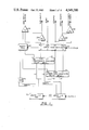
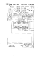
- FIG. 1 illustrates a block diagram of the multiplier implementation.
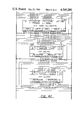
- FIG. 2 presents the detailed block diagram of the 6 ⁇ 6 multiply with parity gate array used in the multiplier of FIG. 1.
- FIG. 3 functionally illustrates an individual carry/save adder used in the logical diagram of FIG. 2.
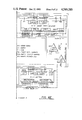
- FIG. 4 pictorially illustrates the function of the 6 ⁇ 6 multiply with parity gate array.
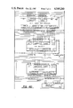
- FIG. 5 shows the detailed logical block diagram of the 6 ⁇ 4 adder tree/register with parity gate array used in the multiplier of FIG. 1.
- FIG. 6 includes FIGS. 6A, 6B, 6C, 6D and 6E, positioned as shown, and taken together they illustrate the detailed logical interconnection of the 6 ⁇ 6 multiplier gate array and the 6 ⁇ 4 adder tree/register gate array to form a 12-bit by 12-bit multiplier.
- FIG. 7 presents a table showing the formation of logical products in the 6 ⁇ 6 multiplier gate arrays for the multiplier of FIG. 6.
- FIG. 8 includes FIGS. 8A and 8B, positioned as shown, and taken together they diagram the use of 12-bit by 48-bit multipliers, adder tree/registers.
- FIG. 1 shows a simplified block diagram of a 12-bit by n-bit multiplier.
- the value of n is assumed to be a multiple of six, which may be achieved by appending zeros onto the data which is to be used as the multiplicand.
- the inputs to the multiplier consist of a 12-bit multiplier held in the Multiplier Register 110, and a n-bit multiplicand, held in the Multiplicand Register 112. These registers are clocked simultaneously via clock signal A. The bits in these registers are numbered starting at 1, from left to right.
- the main outputs of the multiplier consist of a n+12 bit Sums word and a n+12 bit Carries word. These two outputs, when added together after shifting the Carries left one position, will form the desired product. Parity information is included with all input and output data and parity checking of the multiplier is performed.
- Each of the lower ranks ( ⁇ and 1) 114 and 118, of the multiplier consists of 6-bit by 6-bit multiplier chips, numbering n/6+1 chips.
- the outputs of these ranks 114, 118 consist of Sums and Carries similar in principal to the overall multiplier outputs, and combined Parity of the Internal, (PIC) and Output (POC) Carries.
- Internal carries are any carries produced in the process of reducing the summands by addition, but which are not accessible to the pins of the individual chips because of pin limitations.
- the Upper Rank 122 of the multiplier consists of 6-bit-wide by 4-bit adder/register chips, numbering n/6+2 chips. This rank 122 reduces the four inputs from the lower ranks 114, 118 to the Sums and Carries which form the final product, and it also produces the Parities of the Internal (PIC) and Output (POC) Carries separately for error detection.
- PIC Internal
- POC Output
- Lower rank ⁇ , 118 is fed the most significant six bits of the Multiplier, bits 1 through 6, and Lower Rank 1, 114 is fed the least significant six bits of the Multiplier, bits 7 through 12.
- the entire Multiplicand 112 is fed to both of the Lower Ranks 114, 118.
- Equations for parity generation are developed as follows.
- Multr stands for Multiplier
- Mpcd Multiplicand
- IC Internal Carries
- OC Output Carries.
- parity of any of the carries, internal or external, is not readily predicted, and is instead generated directly from the carries inside each chip.
- External parity generators 124, 126 are labeled PG in FIG. 1, and parity checkers 128, 130 which detect single bit errors, are labeled PC.
- the PC and PG functions are logically identical, and are circuits which perform multiple-bit exclusive-OR functions.
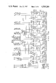
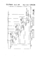
- FIG. 2 shows the internal structure 200 of the 6-bit by 6-bit multiply circuits which are used to build structures 114, 118 of FIG. 1.
- the triangular structures 250, 254, 258, 262, 268, 272, 276, 278 and 280 represent parity generators with the same function as in the previous discussion. These circuits are well known in the art and require no further discussion.
- the trapezoidal structures 300 represent carry-save adders, each of whose function will be later described in conjunction with FIG. 3.
- the entire multiplicand is multiplied by each digit of the multiplier. This causes the formation of as many partial products as there are digits in the multiplier.
- the multiplicand is merely copied for non-zero multiplier bits, and all zeros are copied for multiplier bits equal to zero.
- the circuit of FIG. 2 generates a 6-bit by 6-bit square of this parallelogram for binary multiplication, and reduces the six rows to two rows termed sums and carries using the network of carry-save adders. There are six columns of four carry-save adders each. The partial product bits are all formed at the inputs to the lowest row of the carry-save adders via AND gates at each adder input. These are not explicitly shown in FIG. 2, but are implied by the structure labeled Adder Control 212. The bits being AND-ed at each input will be later detailed in FIG. 4.
- the man inputs to the circuit chip are the 6-bit Multiplier 208 entering Adder Control 212 which implies the generation of six rows of partial products, and the 11-bit Multiplicand 210. Eleven bits are required since eleven different Multiplier bits participate in a 6-bit wide slice of the partial product parallelogram as the Multiplicand is left-shifted five times. This is also illustrated in FIG. 4.
- the main outputs of the circuit chip are six Sum bits, (noted as out sum 1 through out sum 6) and six Carry bits, (out cy1 through out cy6). When added together as shown in the lower portion of FIG. 4 below the summation bar, along with the Stage Carries to be discussed later, these form the sum of the six original rows of partial products.
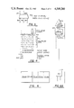
- FIG. 3 illustrates the function of a single carry-save adder 300.
- the function of this structure is to add together three input bits of equal weight x, y, and z to produce a two-bit output sum.
- the most significant bit of this sum is termed the Carry bit, and the least significant bit is termed the Sum bit.
- Carry bit The most significant bit of this sum
- Sum bit The least significant bit is termed the Sum bit.
- Generalized Boolean equations for these bits are also shown in FIG. 3.
- each column of four carry-save adders reduces a column of six partial product bits to two bits, a Sum and a Carry Sn, Cn.
- Internal carries are allowed to propagate only to the next-highest order column when passing through each of the three ranks of adders in the circuit chip. Carries leaving the highest-order column and entering the lowest-order column are termed Stage Carries. These are provided as pins on the circuit chip to allow unlimited extension of the three adder ranks for wider multiplicands.
- the parity of the internal carries and output stage carries, the parity of the output carries, and their combined parity is also generated and sent to output pins for error checking.
- FIG. 4 illustrates the function of the 6-bit by 6-bit multiplier chip.
- the generation of the 6-bit square slice of the partial product parallelogram is also shown in FIG. 4.
- the Multiplier and Multiplicand bits are numbered to correspond with FIG. 2.
- Each Multiplier bit is AND-ed with each of the Multiplicand bits on its row.
- FIG. 4 illustrates the manner in which the output Sums, Carries, and Stage Carries are aligned before addition to produce the sum of the six partial product rows.
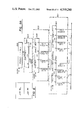
- FIG. 5 shows the internal organization of the 6-bit wide by 4-bit adder/register circuit chip 500.
- This circuit chip 500 reduces four summands A, B, C, and D to two numbers, also termed Sums and Carries, using a network of carry-save adders 512 to 534, as in the multiplier circuit chip. In this case, only four rows A, B, C and D of data are being reduced, so that two ranks of adders are sufficient. Again, carries from the lower rank are allowed to propagate only to the next highest-order column of adders.
- Stage Carries leaving the first rank of adders from the highest-order column 512 and entering the second rank of adders in the lowest-order column 534 are termed Stage Carries. Pins are provided for the Stage Carries to allow unlimited extension of the adder/register structure.
- the main inputs to the adder/register chip 500 are the four Summands, named A, B, C, and D, each consisting of six bits numbered 1-6.
- the like-numbered bits of each Summand are applied to the same column of adders.
- the outputs of the second rank of adders 524, 526, 528, 530, 532 and 534 are six sum bits and six carry bits which are captured in twelve bits of a latch register 540 located on the circuit chip.
- Parity of the internal carries and the output Stage Carry is generated and latched in the remaining bit of the 13-bit latch register 540.
- the main outputs of the circuit chip are the Sum and Carry output signals and the parity of the output Carries which is generated on the circuit chip directly from the register outputs via parity generator 542.
- the Sum and Carry outputs 544, 546 and internal carry parity 548 come directly from the latch register 540.
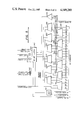
- FIG. 6A through FIG. 6E when arranged as shown in FIG. 6, illustrates the detailed interconnection of the Multiplier 610 and Multiplicand 612 registers, the two Lower Ranks of 6-bit by 6-bit multiplier chips 200, the Upper Rank of 6-bit by 4-bit adder/register chips 500, and external error detection gating necessary to build a 12-bit by 12-bit multiplier.
- a 24-bit full binary adder may be used to add the output Sums from the Upper Rank to the left-shifted output Carries from the Upper Rank. This adder is not shown.
- FIG. 6A through FIG. 6E when arranged as shown in FIG. 6, further clearly illustrates how the Carry outputs from each of the Lower Ranks ⁇ and 1 are, in effect, left-shifted before being fed forward to the Upper Rank.
- bit 1 of the Carries is not connected to any subsequent logic for any of the ranks. This is because these Carry bits will always be zero if the multiply array is connected in this scheme. If these bits were non-zero, the product would be forced to be one bit wider than is mathematically possible for a given rank.
- Another point is that the Stage Carries out of the left end of any given rank are also left unconnected for the same reason.
- the relationship of the Lower Ranks ⁇ and 1 to the Upper Rank and to each other is also clearly shown.
- the Lower Ranks ⁇ and 1 are offset from each other by six bit positions, since each takes a separate but adjacent six-bit slice of the Multiplier.
- Each of the Lower Ranks ⁇ and 1 takes identical Multiplicand connections as shown. The scheme of these connections will be better understood when studying FIG. 7.
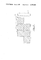
- FIG. 7 shows a chart of how the partial products are formed in each of the Lower Ranks and the necessary Multiplier and Multiplicand connections for the 12-bit by 12-bit multiplier of FIG. 6A through 6E.
- This chart can be extended to show the necessary connections for a 12-bit by n-bit multiplier where n is a multiple of 6. Note that this chart is reversed top-for-bottom with respect to the logical connection scheme of FIG. 6A through 6E, to present its information in a natural mathematical sense.
- FIG. 7 illustrates how the multiplication operation may be thought of as taking shifted copies of the Multiplicand 710, ANDing each of the shifted copies with a particular bit of the Multiplier 712, and summing the resultant logical products.
- Each of the six-bit square areas 714, 716, 718, 720, 722, 724 outlined in FIG. 7 represents the area of logical products covered by a single 6-bit by 6-bit multiply chip.
- FIG. 8A and FIG. 8B when positioned as shown in FIG. 8, when taken together diagrams the use of a 12-bit by 48-bit multipliers, adder tree/registers, and full binary adders to form a 48-bit by 48-bit multiplication pipeline.
- the pipeline implementation shown is designed to multiply a 48-bit Multiplier 810 and a 48-bit Multiplicand 812 to form a 96-bit Product. Since this is a pipeline, a new Product may be formed at the clock cycle rate of the pipeline.
- Each of the first structure type A's included in dotted area 801 consists of two ranks of 6-bit by 6-bit multiply circuit chips and one rank of 6-bit by 4-bit adder/register chips as shown in FIG. 1 and FIG. 6A through 6E.
- the ranks of multiply circuit chips are nine chips wide, and the rank of adder/register chips is ten chips wide. These structures form the original 48 partial product rows, and reduce them to 8 partial product rows.
- Each of the second structure type B's included in dotted area 802 consists of a rank of twelve 6-bit by 4-bit adder/register chips, interconnected as shown in FIG. 6A through 6E. These structures reduce the 8 rows of partial products to 4 rows. Structure type C 826 shown in dotted area 803 is a similar arrangement of sixteen adder/register chips, and reduces the 4 remaining partial product rows to 2 rows.
- Structure type D, 828 shown in dotted area 804 is an ordinary full binary adder, which reduces the two remaining partial products to the final product.
- the inputs to a multiplier consists of a 12-bit multiplier (MULTR) and an n-bit multiplicand (MPCD); outputs consist of an n+12 bit sum word (SUM) and an n+12 bit carry word (CY). Parity is included with all input and output data.
- Ranks ⁇ and 1 gate arrays each consist of (n+6)/6 chips, and perform n-bit X 6-bit multiplies.
- Outputs consist of an n+6 bit sum word and an n+6 bit carry word, and the parity of all carries generated (P IOC ).
- the higher rank of gate arrays consists of (n+12)/6 chips, and sums four n+12 bit input words resulting in an n+12 bit sum word and an n+12 bit carry word, which are then latched. Parity of the internal carries (P IC ) and of the output carry word (P OC ) are also provided.
- the inputs to the higher rank of gate arrays consists of the sum and carry outputs of ranks ⁇ and 1 of lower gate arrays.
- the outputs of rank ⁇ are logically shifted left six positions relative to those from rank 1 before being fed to the next higher rank.
- the sum and carry words from this higher rank may be summed using a full binary adder to completely resolve the n+12 bit product. If a multiplier of arbitrary size is desired, subsequent ranks of these chips followed by a full binary adder may be used.
- the carry parity (internal or output) is not predictable at any point, but is generated directly from the carries inside each circuit chip. Parity may be generated directly from data using a parity generator (PG) and checked using a parity checker (PC). These functions are logically identical, and are exclusive-OR functions.
- PG parity generator
- PC parity checker
- the lower level gate array forms a six bit by six bit square slice of the parallelogram of logical products formed in a binary multiplication.
- Inputs include 11 bits of multiplicand and six bits of multiplier; outputs include a six bit sum word and a six bit carry word.
- Internal to the circuit chip is a tree of carry/save adders. Logical products are formed at the inputs to a first rank of carry-save adders. Stage carry inputs and outputs for extending the carry-save adder array beyond circuit chip boundaries are provided. The parity of the internal carries, output carries and their combination are provided for error checking.
- the circuit chip reduces four six-bit summands to two six-bit outputs.
- Inputs include four six-bit summands: A1-A6, B1-B6, C1-C6 and D1-D6.
- Outputs include a six-bit sum with a six-bit carry.
- the circuit consists of a six-bit wide, four-bit deep carry-save adder tree followed by a latch which captures the six-bit sum and six-bit carry outputs of the adder tree and the parity of the carries generated in the adder tree.
- the internal carry parity (latched) and the output parity (taken from the latch outputs) are again provided for error checking.
Landscapes
- Engineering & Computer Science (AREA)
- Physics & Mathematics (AREA)
- General Physics & Mathematics (AREA)
- Theoretical Computer Science (AREA)
- Computational Mathematics (AREA)
- Mathematical Analysis (AREA)
- Mathematical Optimization (AREA)
- Pure & Applied Mathematics (AREA)
- General Engineering & Computer Science (AREA)
- Computing Systems (AREA)
- Quality & Reliability (AREA)
- Complex Calculations (AREA)
Priority Applications (4)
| Application Number | Priority Date | Filing Date | Title |
|---|---|---|---|
| US06/451,130 US4549280A (en) | 1982-12-20 | 1982-12-20 | Apparatus for creating a multiplication pipeline of arbitrary size |
| JP58234437A JPS59116853A (ja) | 1982-12-20 | 1983-12-14 | 任意サイズの乗算パイプラインを創り出す装置 |
| DE8383307696T DE3381262D1 (de) | 1982-12-20 | 1983-12-19 | Modulare hochgeschwindigkeitsmultiplizierer, und integrierte schaltungs-modulen fuer solche multiplizierer. |
| EP83307696A EP0112186B1 (en) | 1982-12-20 | 1983-12-19 | Modular high-speed multipliers, and integrated circuit chip modules for such multipliers |
Applications Claiming Priority (1)
| Application Number | Priority Date | Filing Date | Title |
|---|---|---|---|
| US06/451,130 US4549280A (en) | 1982-12-20 | 1982-12-20 | Apparatus for creating a multiplication pipeline of arbitrary size |
Publications (1)
| Publication Number | Publication Date |
|---|---|
| US4549280A true US4549280A (en) | 1985-10-22 |
Family
ID=23790932
Family Applications (1)
| Application Number | Title | Priority Date | Filing Date |
|---|---|---|---|
| US06/451,130 Expired - Lifetime US4549280A (en) | 1982-12-20 | 1982-12-20 | Apparatus for creating a multiplication pipeline of arbitrary size |
Country Status (4)
| Country | Link |
|---|---|
| US (1) | US4549280A (ja) |
| EP (1) | EP0112186B1 (ja) |
| JP (1) | JPS59116853A (ja) |
| DE (1) | DE3381262D1 (ja) |
Cited By (5)
| Publication number | Priority date | Publication date | Assignee | Title |
|---|---|---|---|---|
| US4752905A (en) * | 1984-11-09 | 1988-06-21 | Hitachi, Ltd. | High-speed multiplier having carry-save adder circuit |
| US4754422A (en) * | 1983-12-28 | 1988-06-28 | Hitachi, Ltd. | Dividing apparatus |
| GB2244829A (en) * | 1989-01-13 | 1991-12-11 | Vlsi Technology Inc | Method for analyzing datapath elements |
| US10873332B2 (en) | 2018-07-12 | 2020-12-22 | Intel Corporation | Adder circuitry for very large integers |
| US11301213B2 (en) | 2019-06-24 | 2022-04-12 | Intel Corporation | Reduced latency multiplier circuitry for very large numbers |
Citations (5)
| Publication number | Priority date | Publication date | Assignee | Title |
|---|---|---|---|---|
| US3508038A (en) * | 1966-08-30 | 1970-04-21 | Ibm | Multiplying apparatus for performing division using successive approximate reciprocals of a divisor |
| US3596072A (en) * | 1968-05-24 | 1971-07-27 | Hitachi Ltd | Error-detecting circuitry in adder system |
| US3670956A (en) * | 1968-09-26 | 1972-06-20 | Hughes Aircraft Co | Digital binary multiplier employing sum of cross products technique |
| US3986015A (en) * | 1975-06-23 | 1976-10-12 | International Business Machines Corporation | Arithmetic unit for use in a digital data processor and having an improved system for parity check bit generation and error detection |
| US4314349A (en) * | 1979-12-31 | 1982-02-02 | Goodyear Aerospace Corporation | Processing element for parallel array processors |
Family Cites Families (2)
| Publication number | Priority date | Publication date | Assignee | Title |
|---|---|---|---|---|
| JPS5395540A (en) * | 1977-02-01 | 1978-08-21 | Nec Corp | Multi-input adder |
| JPS5523518A (en) * | 1978-08-02 | 1980-02-20 | Nippon Telegr & Teleph Corp <Ntt> | Adder circuit having error check and correction function |
-
1982
- 1982-12-20 US US06/451,130 patent/US4549280A/en not_active Expired - Lifetime
-
1983
- 1983-12-14 JP JP58234437A patent/JPS59116853A/ja active Pending
- 1983-12-19 EP EP83307696A patent/EP0112186B1/en not_active Expired
- 1983-12-19 DE DE8383307696T patent/DE3381262D1/de not_active Expired - Fee Related
Patent Citations (5)
| Publication number | Priority date | Publication date | Assignee | Title |
|---|---|---|---|---|
| US3508038A (en) * | 1966-08-30 | 1970-04-21 | Ibm | Multiplying apparatus for performing division using successive approximate reciprocals of a divisor |
| US3596072A (en) * | 1968-05-24 | 1971-07-27 | Hitachi Ltd | Error-detecting circuitry in adder system |
| US3670956A (en) * | 1968-09-26 | 1972-06-20 | Hughes Aircraft Co | Digital binary multiplier employing sum of cross products technique |
| US3986015A (en) * | 1975-06-23 | 1976-10-12 | International Business Machines Corporation | Arithmetic unit for use in a digital data processor and having an improved system for parity check bit generation and error detection |
| US4314349A (en) * | 1979-12-31 | 1982-02-02 | Goodyear Aerospace Corporation | Processing element for parallel array processors |
Non-Patent Citations (4)
| Title |
|---|
| Lai et al., "Logic Networks of Carry-Save Adders", IEEE Trans. on Computers, vol. C-31, No. 9, Sep. 1982, pp. 870-882. |
| Lai et al., Logic Networks of Carry Save Adders , IEEE Trans. on Computers , vol. C 31, No. 9, Sep. 1982, pp. 870 882. * |
| Partridge, "Cascade Adder for Multiply Operations", IBM Tech. Disclosure Bulletin, vol. 13, No. 8, Jan. '71, pp. 2406-2407. |
| Partridge, Cascade Adder for Multiply Operations , IBM Tech. Disclosure Bulletin, vol. 13, No. 8, Jan. 71, pp. 2406 2407. * |
Cited By (7)
| Publication number | Priority date | Publication date | Assignee | Title |
|---|---|---|---|---|
| US4754422A (en) * | 1983-12-28 | 1988-06-28 | Hitachi, Ltd. | Dividing apparatus |
| US4752905A (en) * | 1984-11-09 | 1988-06-21 | Hitachi, Ltd. | High-speed multiplier having carry-save adder circuit |
| GB2244829A (en) * | 1989-01-13 | 1991-12-11 | Vlsi Technology Inc | Method for analyzing datapath elements |
| GB2244829B (en) * | 1989-01-13 | 1993-01-13 | Vlsi Technology Inc | Method for analyzing datapath elements |
| US10873332B2 (en) | 2018-07-12 | 2020-12-22 | Intel Corporation | Adder circuitry for very large integers |
| US11662979B2 (en) | 2018-07-12 | 2023-05-30 | Intel Corporation | Adder circuitry for very large integers |
| US11301213B2 (en) | 2019-06-24 | 2022-04-12 | Intel Corporation | Reduced latency multiplier circuitry for very large numbers |
Also Published As
| Publication number | Publication date |
|---|---|
| JPS59116853A (ja) | 1984-07-05 |
| EP0112186A3 (en) | 1986-10-15 |
| EP0112186B1 (en) | 1990-02-28 |
| EP0112186A2 (en) | 1984-06-27 |
| DE3381262D1 (de) | 1990-04-05 |
Similar Documents
| Publication | Publication Date | Title |
|---|---|---|
| US5325320A (en) | Area efficient multiplier for use in an integrated circuit | |
| Ma et al. | Multiplier policies for digital signal processing | |
| Parhami | Carry-free addition of recoded binary signed-digit numbers | |
| Anderson et al. | The IBM system/360 model 91: Floating-point execution unit | |
| US5787029A (en) | Ultra low power multiplier | |
| US4228520A (en) | High speed multiplier using carry-save/propagate pipeline with sparse carries | |
| US4168530A (en) | Multiplication circuit using column compression | |
| US4489393A (en) | Monolithic discrete-time digital convolution circuit | |
| US4780842A (en) | Cellular processor apparatus capable of performing floating point arithmetic operations | |
| US5253195A (en) | High speed multiplier | |
| US3795880A (en) | Partial product array multiplier | |
| US5126964A (en) | High performance bit-sliced multiplier circuit | |
| US5010511A (en) | Digit-serial linear combining apparatus useful in dividers | |
| KR100308726B1 (ko) | 고속 산술 장치에서 올림수 예견가산기 스테이지의 수를 감소시키는 장치 및 방법 | |
| US6434586B1 (en) | Narrow Wallace multiplier | |
| US4796219A (en) | Serial two's complement multiplier | |
| US4549280A (en) | Apparatus for creating a multiplication pipeline of arbitrary size | |
| US4700325A (en) | Binary tree calculations on monolithic integrated circuits | |
| US4545028A (en) | Partial product accumulation in high performance multipliers | |
| US5257217A (en) | Area-efficient multiplier for use in an integrated circuit | |
| US4523210A (en) | Fast error checked multibit multiplier | |
| US5677863A (en) | Method of performing operand increment in a booth recoded multiply array | |
| US5126965A (en) | Conditional-sum carry structure compiler | |
| US5283755A (en) | Multiplier employing carry select or carry look-ahead adders in hierarchical tree configuration | |
| EP0529755B1 (en) | Method and apparatus for negating an operand of a multiplication operation |
Legal Events
| Date | Code | Title | Description |
|---|---|---|---|
| AS | Assignment |
Owner name: SPERRY CORPORATION, 1290 AVENUE OF THE AMERICAS, N Free format text: ASSIGNMENT OF ASSIGNORS INTEREST.;ASSIGNOR:SCHOMBURG, JOHN R.;REEL/FRAME:004428/0402 Effective date: 19821215 |
|
| STCF | Information on status: patent grant |
Free format text: PATENTED CASE |
|
| FPAY | Fee payment |
Year of fee payment: 4 |
|
| FEPP | Fee payment procedure |
Free format text: PAYOR NUMBER ASSIGNED (ORIGINAL EVENT CODE: ASPN); ENTITY STATUS OF PATENT OWNER: LARGE ENTITY |
|
| FPAY | Fee payment |
Year of fee payment: 8 |
|
| FPAY | Fee payment |
Year of fee payment: 12 |