US4677622A - Error correction method and system - Google Patents
Error correction method and system Download PDFInfo
- Publication number
- US4677622A US4677622A US06/622,711 US62271184A US4677622A US 4677622 A US4677622 A US 4677622A US 62271184 A US62271184 A US 62271184A US 4677622 A US4677622 A US 4677622A
- Authority
- US
- United States
- Prior art keywords
- words
- flags
- error
- decoding
- circuit
- Prior art date
- Legal status (The legal status is an assumption and is not a legal conclusion. Google has not performed a legal analysis and makes no representation as to the accuracy of the status listed.)
- Expired - Lifetime
Links
- 238000012937 correction Methods 0.000 title claims abstract description 65
- 238000000034 method Methods 0.000 title claims description 39
- 208000011580 syndromic disease Diseases 0.000 claims description 40
- 230000015654 memory Effects 0.000 claims description 34
- 230000004044 response Effects 0.000 claims description 4
- 230000014509 gene expression Effects 0.000 description 31
- 238000010586 diagram Methods 0.000 description 22
- 239000000872 buffer Substances 0.000 description 10
- 238000001514 detection method Methods 0.000 description 8
- 230000005540 biological transmission Effects 0.000 description 7
- 238000006243 chemical reaction Methods 0.000 description 7
- 230000009191 jumping Effects 0.000 description 6
- 239000002131 composite material Substances 0.000 description 5
- 239000011159 matrix material Substances 0.000 description 2
- 238000012545 processing Methods 0.000 description 2
- 230000001360 synchronised effect Effects 0.000 description 2
- 108091005425 Sr-CI Proteins 0.000 description 1
- 102220536910 Transcription factor JunD_F32A_mutation Human genes 0.000 description 1
- 230000005856 abnormality Effects 0.000 description 1
- 238000004891 communication Methods 0.000 description 1
- 238000007796 conventional method Methods 0.000 description 1
- 125000004122 cyclic group Chemical group 0.000 description 1
- 230000003247 decreasing effect Effects 0.000 description 1
- 238000005516 engineering process Methods 0.000 description 1
- 238000004519 manufacturing process Methods 0.000 description 1
- 230000002265 prevention Effects 0.000 description 1
- 102220139828 rs587782481 Human genes 0.000 description 1
- 238000005070 sampling Methods 0.000 description 1
Images




Classifications
-
- G—PHYSICS
- G11—INFORMATION STORAGE
- G11B—INFORMATION STORAGE BASED ON RELATIVE MOVEMENT BETWEEN RECORD CARRIER AND TRANSDUCER
- G11B20/00—Signal processing not specific to the method of recording or reproducing; Circuits therefor
- G11B20/10—Digital recording or reproducing
- G11B20/18—Error detection or correction; Testing, e.g. of drop-outs
- G11B20/1806—Pulse code modulation systems for audio signals
- G11B20/1809—Pulse code modulation systems for audio signals by interleaving
Definitions
- the present invention relates to error correction in an apparatus for reproducing a digital signal and, more particularly, to an error correction method and a system which are suitable for decoding code words having a number of check words, such as in the decoding of Reed Solomon Codes.
- check words are added when transmitting or recording and the error data is corrected using those check words upon reception or reproduction.
- BCH codes and the like which have good efficiency and can be easily decoded are used.
- Reed Solomon codes as one type of the BCH codes are usually used as the block codes.
- cross-interleave codes are known as a method of increasing the correcting capability by performing double encoding by the use of these codes.
- FIGS. 1 and 2 show well-known examples of an encoding circuit and a decoding circuit for the cross-interleave Reed Solomon codes (hereinbelow, abbreviated as CIRC codes), which circuits are respectively disclosed in GB No. 2076569A (Odaka et al, U.S. Pat. No. 4,413,340), and in BG No. 2079993A (Sako et al, U.S. Pat. No. 4,437,185).
- numerals 1 and 2 denote encoders
- 3, 4 and 5 indicate interleave circuits
- 6 represents a data inverting circuit.
- numerals 7 and 8 denote decoders
- 9, 10 and 11 are deinterleave circuits.
- the double encoding by the use of Reed Solomon codes is performed.
- the coding circuit of FIG. 1 after the first interleave was performed by the interleave circuit 3 with respect to 24 information words, check words Q 1 , Q 2 , Q 3 and Q 4 of four words are added by the encoder 1. Further, after the second interleave was performed by the interleave circuit 4 with regard to the code block of 28 words consisting of the 24 information words and four check words, check words P 1 , P 2 , P 3 , and P 4 of four words are added by the encoder 2.
- the code block of 32 words consisting of 24 information words and eight check words is further subjected to the third interleave processing by the interleave circuit 5, and thereafter they are converted to serial data and this data is then transmitted or recorded.
- the check words are inverted by the data inverting circuit 6 for prevention of misdetection or miscorrection when sequential data is lost.
- the first decoding is done by the decoder 7.
- the error detection and error correction by use of the check words P 1 to P 4 are executed.
- the 24 information words and four check words to which the error detection and error correction were done by the decoder 7 are deinterleaved .by the deinterleave circuit 10 corresponding to the foregoing second interleave, thereafter they are subjected to the second decoding by the decoder 8.
- the error detection and error correction are performed by use of the check words Q 1 to Q 4 .
- the 24 information words to which the error detection and error correction were done by the decoder 8 are deinterleaved by the deinterleave circuit 11 corresponding to the above-mentioned first interleave, then they are outputted.
- the correcting capability can be raised by performing the decoding twice or more times by use of two different code blocks (P 1 -P 4 ; Q 1 -Q 4 ).
- the technology for raising the error correction capability is disclosed in GB No. 2079993A (U.S. Pat. No. 4,437,185 issued Mar. 13, 1984).
- the conventional decoding method only one or two words are corrected in the first decoding C 1 and the second decoding C 2 , so that the correcting capability which the codes inherently have is not sufficiently made the most of.
- the optimum decoding method in accordance with the state of flag upon the first decoding is not employed in the second decoding.
- the fundamental concept of the present invention is that in case of correcting the errors of p-words in the codes having a Hamming distance of d and in case of correcting the erasures of q-words in the same codes, plural decoding methods so as to satisfy the relation
- the above decoding method is implemented by an error correcting system using programs.
- FIG. 1 is a diagram showing a prior art coding circuit for the CIRC codes
- FIG. 2 is a diagram showing a prior art decoding circuit for the CIRC codes
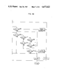
- FIG. 3 is a schematic flowchart showing the second decoding procedure for the CIRC codes according to the invention.
- FIGS. 4, 4A, 4B and 5, 5A, 5B show detailed flowcharts of FIG. 3;
- FIG. 6 is a block diagram showing a reproducing apparatus in which a system according to an embodiment of the present invention is incorporated;
- FIGS. 7, 7A and 7B show a timing chart for error correction
- FIG. 8 is a block diagram of an error correction system according to an embodiment of the invention.
- FIG. 9 is a diagram showing a syndrome generating circuit
- FIG. 10 is a diagram showing a multiplying/dividing circuit over GF (2 8 );
- FIG. 11 is a diagram showing an adder over GF (2 8 );
- FIG. 12 is a diagram showing the program arrangement
- FIGS. 13, 13A and 13B show one embodiment of the error correcting system of the invention
- FIG. 14 is a diagram showing an arithmetic logic circuit over Galois field
- FIG. 15 is a diagram showing the program arrangement
- FIGS. 16, 16A and 16B show another embodiment of the error correcting system of the invention.
- FIG. 17 is a diagram showing an example of an arrangement of the multiplying circuit which is used in the invention.
- FIG. 18 is a diagram showing the dividing circuit which is suitable for use in the invention.
- FIG. 19 is a diagram showing the arithmetic logic circuit for performing the composite operations which is suitable for use in the invention.
- FIG. 20 shows a comparison diagram regarding the correcting capabilities by the present invention and the conventional example.
- the set ⁇ 0, 1, ⁇ , ⁇ 2 , . . . , ⁇ 254 ⁇ of which the (2 8 -2) elements which are represented by the power of ⁇ were added to the elements of GF (2) constitutes GF (2 8 ).
- the word length n can be reduced within a range of
- a Hamming distance d is (2t+1) in these Reed Solomon codes.
- the error locations ⁇ i can be obtained by solving expression (9). Further, by obtaining these error locations ⁇ i and error values e i .sbsb.1, e i .sbsb.2, . . . e i ⁇ from expression (7) to obtain E(x), the error correction can be performed by
- the error correction can be performed within a range of
- the error values e i .sbsb.1, e i .sbsb.2 and e i .sbsb.3 can be obtained from
- the error correction can be efficiently performed by use of the combination of these decoding methods.
- the number of check words is four and the Hamming distance is five.
- the error correction is performed and, at the same time such flags are added to each word.
- the reason why a plurality of flags are added in this way is that probabilities of misdetection and miscorrection which are caused upon decoding differ in dependence upon the respective cases. As the correcting capability is higher, the probabilities of misdetection and miscorrection become larger. Assuming that these probabilities are P(F i ),
- the error locations can be detected by use of the flags added in the first decoding. Consequently, the following three kinds of correcting methods are considered. ##EQU20##
- the errors of up to four words to which the flags were added can be corrected.
- this method has the highest correcting capability, if there are errors to which no flags are added due to the misdetection or miscorrection in the first decoding in the correction block, miscorrection will have occurred.
- the error flag the flag such as F 0 of which the probability of misdetection and miscorrection is low.
- the detecting capability can be raised due to the checking of syndromes or by other correcting method.
- the two words (or one word) to which the F 1 flags were added are regarded as the error words and the error location of one word is detected.
- the error location detected coincides with the location of the F 1 flag or where no error is detected, the error correction of three or less words is performed.
- the error detecting capability can be improved by further finely checking in dependence upon the states of the F 2 flags.
- N(F 0 ), N(F 1 ) and N(F 2 ) respectively indicate the numbers of words to which the F 0 flag, F 1 flag and F 2 flag were added
- N(E) denotes the number of errors detected by the decoding
- L(N 0 ), L(F 1 ) and L(F 2 ) represent the numbers of words to which the respective flags were added among the error locations detected.
- N(F 0 ) and N(F 1 ) are checked for determination with respect to which decoding should be performed.
- the error correcting capability can be raised as compared with the conventional method whereby the error correction of up to two words is done.
- the error correcting capability can be also raised by the use of an optimum decoding method in accordance with the state of the flag. For this purpose, selection of such an optimum decoding method is made such that both (a) the error correcting capability determined from the probability of addition of flags and that of failure of error detection at the first decoding and the probability of failure of error correction and that of failure of error detection at the second decoding and (b) the error detection capability are enhanced thereby.
- the error correcting method of invention can be also applied to other decoding than the CIRC codes, for example, to the case where the cyclic codes (CRC codes) are used for production of the second check words and only the error detection is performed in the first decoding.
- CRC codes cyclic codes
- FIG. 6 shows a block diagram of the reproducing apparatus, in which a reference numeral 115 denotes a digital signal reproducing circuit; 116 is a data storing circuit; 117 an error correcting system according to the present invention; 118 a flag storing circuit; 119 an error concealing circuit; 120 a D/A converter; and 121 a control circuit.
- the digital signal reproducing circuit 115 reproduces the digital signal from the reproduction signal input from an input terminal 112 and outputs it to a bus line 114, and at the same time it detects the sync signal in the reproduction signal and outputs it to the control circuit 121.
- the data storing circuit 116 temporarily stores the digital signal reproduced and an RAM is generally used.
- the deinterleave is performed by controlling the write addresses and read addresses of this storing circuit 116.
- the error correcting system 117 performs the first decoding and the second decoding.
- the flag storing circuit 118 temporarily stores the flags added on a frame unit basis by the first decoding and an RAM is generally used.
- the error concealing circuit 119 conceals, by means of mean value interpolation or the like, the words which were determined to be uncorrectable in the second decoding which is carried out by the error correcting system 117.
- the digital signal is converted to the analog signal by the D/A converter 120 and is outputted to an output terminal 113.
- the control circuit 121 controls each section by use of the sync signals detected by the digital signal reproducing circuit and the master clock output from an oscillator 122 as a reference.
- a numeral 126 denotes a data output timing to the D/A converter 120. Namely, it is necessary to perform the D/A conversion at a constant period determined by the sampling frequency irrespective of other operations. Therefore, it is necessary to execute the reception and transmission of the data among the digital signal reproducing circuit 115, error correcting apparatus 117 and data storing circuit 116 at other time than the time of outputting the data. Also, a sync signal 127 is used as a reference signal upon data input and error correction.
- the data reproduced by the digital signal reproducing circuit 115 is first inputted to the data storing circuit 116 and to a data input/output terminal 123 of the error correcting system 117 in the interval indicated at 129 of FIGS. 7A and 7B. At this time, the data locations (0 to 31) corresponding to the input data are inputted to a location input/output terminal 124 of the error correcting system 117.
- the first decoding is performed in the interval 132 with regard to the data of 132 words inputted in the interval 129.
- the data stored in the data storing circuit 116 is corrected in the interval 128 in the next frame using the decoded result.
- the flag data is outputted from a flag input/output terminal 125 and is stored in the flag storing circuit 118.
- the data which is subjected to the second decoding is inputted in the interval 132. Namely, the data of 28 words is inputted from the data storing circuit 116 in the interval 128. At this time, the data locations (0 to 27) corresponding to the input data are inputted to the location input/output terminal 124.
- the second decoding is performed in the interval 129 in the next frame.
- the data stored in the data storing circuit 116 is corrected in the interval 131 in the next frame using the decoded result.
- the uncorrectable flag which is used when the correction is impossible in the second decoding is outputted in the interval 130.
- This uncorrectable flag is written in the location of the data storing circuit 116 where the check words have been written and is read out simultaneously when the data is outputted to the D/A converter.
- the error concealment is performed by the error concealing circuit 119.
- the data transferring operation and decoding operation can be carried out at a low speed.
- FIG. 8 shows a block diagram of the error correcting system.
- numerals 17 to 19 denote bus lines; 20 is a syndrome generating circuit; 21 and 22 are ROMs; 25, 27 and 29 are RAMs; 24 an arithmetic logic circuit; 26 a counter; 28 a comparator; 30 a conditional judging circuit; 31 a program ROM; and 32 an address counter.
- This circuit comprises: the three bus lines; the circuits connected to these bus lines; and a control circuit for controlling the operations of the respective circuits in accordance with the program.
- the bus line 17 is the data bus for reception and transmission of the reception signal and data such as error patterns and the like.
- the bus line 18 is the location bus for reception and transmission of the data such as the locations of the data and the like.
- the bus line 19 is the flag bus for reception and transmission of the data regarding the flags which are added to the data.
- a data input/output terminal 12, a location input/output terminal 13 and a flag input/output terminal 14 are connected to each bus, respectively.
- the syndrome generating circuit 20 produces the syndromes S 0 to S 3 on the basis of the reception signals inputted from the data input/output terminal 12.
- the syndrome generating circuit 20 is constituted by circuits as shown in FIG. 9.
- a numeral 42 is an EOR circuit and 44 is an eight-bit latch.
- a numeral 43 is a matrix arithmetic logic circuit: in which the product of "1" and the input signal is outputted from the S 0 forming circuit; the product of " ⁇ " and the input signal is outputted from the S 1 generating circuit, the product of " ⁇ 2 " and the input signal is outputted from the S 2 generating circuit; and the product of " ⁇ 3 " and the input signal is outputted from the S 3 generating circuit.
- FIG. 9 An example of the S 1 generating circuit is shown in FIG. 9.
- a reception signal is inputted to an input terminal 38 of this circuit and a clock signal synchronized with the reception signal is inputted to a clock input terminal 40 of the latch 44, so that the syndrome is outputted from an output terminal 39 at the end of input of the reception signal.
- a clear signal input terminal 41 is used to clear the latch before producing the syndrome.
- the arithmetic logic circuit 24 serves to perform the operation to obtain the error locations and error patterns by use of the syndromes S 0 to S 3 produced by the syndrome generating circuit 20.
- the multiplication, division and addition over GF (2 8 ) are executed.
- FIG. 10 shows an example of the multiplying/dividing circuit which is included in the arithmetic logic circuit 24.
- ROMs 48 and 49 respectively output x and y for X and Y which are fed to input terminals 45 and 46.
- An adding/subtracting circuit 50 performs the addition in case of the multiplication and performs the subtraction in case of the division.
- An ROM 51 outputs ⁇ x ⁇ y to an output terminal 47 for the output (x ⁇ y) of the adding/subtracting circuit 50.
- the addition over GF (2 8 ) may be done by performing the addition of mod 2 for every bit.
- the RAM 25 serves to store the syndromes S 0 to S 3 and the arithmetic operation results by the arithmetic logic circuit 24. Also, an eight-input OR circuit 23 acts to discriminate whether the data of the data bus 17 is "0" or not.
- the ROM 21 performs the conversion from i to ⁇ i
- the ROM 22 performs the conversion from ⁇ i to i.
- the counter 26 counts the number of flags in one block.
- the numbers of F 0 , F 1 and F 2 are counted by the counter 26 and those numbers are compared with predetermined numbers by the comparator 28, thereby making the determination with respect to how many words are corrected, or that whether the correction is done or the uncorrectable state is set without correcting, and the like.
- the RAM 27 stores the number of flags counted by the counter 26, error locations, etc. Also, the comparator 28 is used to compare the above-mentioned number of flags with a predetermined number, and the data during the decoding processing with constants.
- the RAM 29 stores the flags F 0 to F 2 representing the results of the first decoding which were added to the data in the second decoding.
- the states of the flags stored in the RAM 29 are used to check the presence and absence of the flag at the error location obtained by the decoding.
- the conditional judging circuit 30 determines the execution of branching of the program on the basis of the discrimination results by the OR circuit 23 and comparator 28 and of the states of the flags stored in the RAM 29.
- the program ROM 31 stores the program for decoding by control of each of the above-mentioned circuits.
- FIG. 12 shows a program arrangement.
- One word of this program consists of 32 bits.
- a numeral 52 is an instruction field (four bits) to select the register for storage of data among the registers included in the input section of each circuit.
- An instruction field (four bits) 53 is used to select the buffer for output of data among the buffers included in the output section of each circuit. The data can be transferred through the bus lines from arbitrary circuits to arbitrary circuits by the instruction fields 52 and 53.
- An instruction field (two bits) 54 is used to write data into the RAM 25 or 27. Since the data is written in the RAM 29 only when the reception signal is inputted, there is no need to control by the program.
- a two-bit instruction field 55 is used to perform the selection and the like of the multiplication and division in the arithmetic logic circuit 24.
- a seven-bit instruction field 33 is used to determine the addresses of RAMs and constants which are inputted to each bus line and comparator.
- a four-bit instruction field 34 is used to determine the jump condition of the program. In the conditional judging circuit 30, the content of the field 34 is compared with the states of the OR circuit 23, comparator 28, RAM 29, etc., thereby determining whether the jumping is performed or not.
- a nine-bit instruction field 35 is used to determine the jump address in case of jumping.
- the CIRC codes can be decoded by a relatively short program of about 400 words.
- the counter 32 acts to control the address of the program. This counter serves to advance the address of the program ROM 31 in response to the clock signal which is inputted from a master clock input 15, thereby allowing the program to be executed. In addition, in case of jumping the program, the jump address 35 is loaded to the counter by a jump instruction 37, thereby jumping the program. In addition, an input terminal 16 is used to input a signal to reset the counter 32 at the start of the program.
- the reception signal is first inputted and the syndromes S 0 to S 3 are produced, and in the second decoding, the number of flags is counted and the states of the flags are stored in the RAM 29.
- the decoding is performed by the program and the error locations and error patterns are obtained, then the error data is corrected by expression (10).
- the flags which are added to the data are outputted from the flag input/output terminal 14.
- each circuit is controlled on the basis of the program it is also possible by merely changing the program, to cope with different error correction codes and decoding method in which the circuit scale is small.
- FIGS. 13A and 13B show an embodiment of the error correcting system of the present invention.
- a numeral 133 denotes a syndrome generating circuit
- 134, 139, 141 and 143 are memories
- 136, 137 and 138 are data converters
- 135 an arithmetic logic circuit over Galois field
- 140 a counter
- 142 a comparator
- 144 a control circuit
- 145 an address counter
- 146 a program memory
- 147 a program latch
- 149 and 151 are registers
- 150 and 152 are buffers.
- the reception signal is first inputted and the syndromes S 0 to S 3 are produced.
- the second decoding the number of flags is counted and the states of the flags are stored in the memories 139, 141 and 143.
- the decoding is then performed on the basis of the program and the error location and error patterns are obtained, thereby correcting the error data by expression (10).
- the flags which are added to the data are outputted from the flag input/output terminal 125.
- the syndrome generating circuit 133 produces the syndromes S 0 to S 3 on the basis of the reception signal inputted from the data input/output terminal 123.
- the syndrome generating circuit 133 is constituted by the circuits as shown in FIG. 9.
- a numeral 42 is the EOR circuit and 44 is the eight-bit latch.
- 43 denotes the matrix arithmetic logic circuit. The product of "1" and the input signal is outputted from the S 0 generating circuit; the product of " ⁇ " and the input signal is outputted from the S 1 generating circuit; the product of " ⁇ 2 " and the input signal is outputted from the S 2 generating circuit; and the product of " ⁇ 3 " and the input signal is outputted from the S 3 generating circuit.
- the reception signal is inputted to the input terminal 38 of this circuit and the clock signal synchronized with the reception signal is inputted to the clock input terminal 40 of the latch 44, so that the syndromes are outputted from the output terminal 39 at the end of inputting of the reception signal.
- the counter 140 counts the number of flags in one block.
- the numbers of F 0 , F 1 and F 2 are counted by the counter 140. These numbers are compared with predetermined numbers by the comparator 142, thereby making the determination with respect to how many words are corrected or whether the correction is performed or the correction is determined to be impossible without performing the correction, and the like.
- the memories 139 and 143 store the information regarding the flags added to the respective words.
- the flag information is written when the data is inputted.
- the information stored in the memory 143 is used to check the error locations detected by the second decoding and the locations where the flags were added.
- the information stored in the memory 139 is used as the uncorrectable flag in case of adding the uncorrectable flag to only the word to which the F 0 flag or F 1 flag was added in the case where the correction is impossible in the second decoding.
- the locations (0 to 28) of the words to which the flags were added are written in the memory 141. These locations are used as the error locations when performing the decoding of q ⁇ 1 in the second decoding.
- the decoding time can be shortened.
- the writing of the flag information into the syndrome generating circuit 133, memory 139, counter 140, and memories 141 and 143 is performed by the control circuit 144 independently of the program operation which will be mentioned later. The data input and decoding operation can be therefore simultaneously executed.
- the decoding is performed by the memories 134 and 141, data converters 136, 137 and 138, and arithmetic logic circuit 135.
- the memory 134 stores the syndromes S 0 to S 3 produced by the syndrome generating circuit 133 and the operation result of the arithmetic logic circuit 135.
- the memory 141 stores the error locations and the number of flags counted by the counter 140.
- the converter 136 is the ROM for converting from i to ⁇ i
- the converter 137 is the ROM for converting from ⁇ i to i.
- ( ⁇ i1-i2 + ⁇ i2-i1 ) is first obtained from ⁇ 1 and ⁇ 2 .
- i 1 and i 2 will be known.
- the value of (i 1 -i 2 ) corresponding to ( ⁇ i1-i2 + ⁇ i2-i1 ) has been stored in the converter 138. This value can be obtained from the above-mentioned corresponding table between i and ⁇ i .
- the arithmetic logic circuit 135 performs the multiplication, division and addition over the Galois field GF (2 8 ).
- This logic circuit 135 is constituted by such circuits as shown in FIG. 14.
- a numeral 167 denotes a circuit to obtain the reciprocal number of Y and an ROM or PLA is used;
- 168 is an MPX circuit;
- 169 is a multiplier which is constituted by an EOR and AND circuits;
- 170 is an adder.
- the addition over the Galois field may be done by performing the EOR operation with respect to each bit.
- the MPX circuit 168 selects Y, the operation of
- the comparator 142 is used to compare the above-mentioned numbers of flags with predetermined numbers and to compare the data during the decoding operation with constants.
- the decoding is performed by controlling the above-mentioned memories 134 and 141, data converters 136, 137 and 138, arithmetic logic circuit 135, comparator 142, registers 149, and buffers 150 in accordance with the program stored in the program memory 146.
- the address counter 145 determines the address of the program and advances the address of the program in response to the clock produced by the control circuit 144.
- the jump control circuit 148 determines the execution of the program jump on the basis of the result discriminated by the OR circuit 154 and comparator 142 and of the states of the flags stored in the memory 143. When jumping, the jump address is loaded to the address counter 145 in accordance with the discrimination result of the jump control circuit 148, thereby changing the address of the program.
- FIG. 15 shows the program arrangement.
- One word consists of 32 bits.
- a register selecting code 172 is used to select the register in which the data is stored among the registers 149 provided in the input section of each circuit.
- a buffer selecting code 171 is used to select the buffer from which the data is outputted among the buffers 150 provided in the output section of each circuit. The data can be transferred through the bus lines from arbitrary circuits to arbitrary circuits by these codes 171 and 172.
- SWE 177 and LWE 178 are used to write the data into the memories 134 and 141, respectively.
- YSEL 179 is used to select the multiplication and division in the arithmetic logic circuit 135.
- BSEL 180 is used to select an MPX circuit 153.
- the instruction field 175 is used to determine the addresses of the memories and the constants which are inputted to each bus line and comparators.
- the instruction field indicated at 174 is used to determine the jump condition of the program.
- the content of the instruction field 174 is compared with the states of an OR circuit 154, comparator 142, memory 143, etc., thereby determining the execution of jump.
- the instruction field 176 is used to determine the jump address when jumping.
- the denominations of the buffers and registers indicate 149 and 150 of FIGS. 16A and 16B.
- codes 7 to 9 are used to make the determination on the basis of the result of comparison by the comparator 142.
- Codes A to F are used to make the determination on the basis of the content of the memory 143 corresponding to the address which is determined in dependence upon the value of the FA register.
- the flag information has been stored in the memory 143 as the two-bit data (0 to 3) as shown below.
- the data correction on the basis of the result of the decoding is also performed in accordance with the program.
- the error locations detected by the decoding are first outputted from the location input/output terminal 124 and the data corresponding to those locations are inputted from the data storing circuit 116.
- the error correction shown in expression (10) is performed by the arithmetic logic circuit 135 and they are again written in the data storing circuit 116.
- the flag information Upon correcting, the flag information is also outputted.
- the flag information is handled as the two-bit data instead of handling the F 0 , F 1 and F 2 flags as they are.
- the flag information as shown below is first stored in the FO register.
- this flag information is outputted from the flag input/output terminal 125 to the flag storing circuit 118. Also, in the second decoding, the uncorrectable flag corresponding to this flag information is written in the data storing circuit 116 at 130 of FIG. 7.
- FIG. 16A and 16B show another embodiment of the error correcting system of the present invention.
- the memory 143 is omitted in the circuit of FIGS. 16A and 16B; this point is different from FIGS. 13A and 13B.
- the flag information is stored in both memories 139 and 143. Therefore, by adding some decoding circuit, the memory can be commonly used. With such a circuit arrangement as shown in FIGS. 16A and 16B, the circuit scale can be more reduced.
- each circuit is controlled in accordance with the program it is also possible, by merely changing the program, to cope with the different error correction codes and decoding method in which the circuit scale is small. Further, the operation speed of the system may be lowered by performing the data input and decoding operations simultaneously.
- This arithmetic logic operation can be implemented by nine AND circuits and nine EOR circuits as shown in FIGS. 16A and 16B.
- a reference numeral 208 denotes an A input terminal; 209 is a B input terminal; and 210 is a C output terminal.
- the reciprocal number of Y is ⁇ .sup.(7-j) and can be obtained by the converting ROM as shown in the below Table._____________________________________________ Address Data_____________________________________________ 000 -- 001 001 010 101 011 110 100 111 101 010 110 011 111 100______________________________________
- FIG. 18 The dividing circuit which is used in the invention is shown in FIG. 18, in which a reference numeral 211 denotes a converting ROM having the content of the above converting table, and 212 is a multiplier shown in FIG.17.
- the arithmetic logic circuit of FIG. 16B is constituted by only one ROM, nine AND circuits and nine EOR circuits, the circuit scale is also small.
- FIG. 19 shows another embodiment of the arithmethic logic circuit for use in the present invention.
- the multiplication and division of X and Y are performed in the multiplier 212 by converting the signal which is inputted to the B input terminal of the multiplier 212 to Y or 1/Y by an MPX 214.
- the number of operations can be reduced by performing the composite operation of multiplication and addition or the composite operation of division and addition.
- FIG. 20 shows an example of comparison in error correcting capability between the present invention and the prior art.
- an axis of abscissa indicates the error rate of the reproduction data and an axis of ordinate represents the error rate after error correction.
- Curve 1 indicates the error correcting capability by the prior art correcting method such as disclosed in the above-mentioned Sako et al, U.S. Pat. No. 4,437,185 and The Journal of The Institute of Electronics and Communication Engineers of Japan, J66-A, pages 284 to 285, March 1983.
- This correcting method is of the type in which only one flag, namely, one pointer code signal is added to each word signal at the initial decoding stage and two errors can be corrected at the subsequent decoding stage.
- Curve 2 represents the characteristics of the error correcting capability in the case where the invention is employed, in which up to three flag can be added to each word signal at the initial decoding stage.
- Curve 2 shows the case where the algorithm is adopted which uses three kinds of correcting methods of error correction, error and erasure correction, and erasure correction at the subsequent decoding stage. It will be appreciated from comparison of the curves 1 and 2 that the errors can be reduced to 1/10 12 by the correction when the error rate is 10 -3 in the former case and that they can be decreased to 1/10 15 under the same condition in the latter case.
Landscapes
- Engineering & Computer Science (AREA)
- Multimedia (AREA)
- Signal Processing (AREA)
- Error Detection And Correction (AREA)
Applications Claiming Priority (6)
| Application Number | Priority Date | Filing Date | Title |
|---|---|---|---|
| JP58110931A JPH0636286B2 (ja) | 1983-06-22 | 1983-06-22 | 誤り訂正方法及び装置 |
| JP58-110931 | 1983-06-22 | ||
| JP58130839A JPS6024650A (ja) | 1983-07-20 | 1983-07-20 | ガロア体上の演算回路 |
| JP58-130839 | 1983-07-20 | ||
| JP21085883A JPS60103562A (ja) | 1983-11-11 | 1983-11-11 | 誤り訂正装置 |
| JP58-210858 | 1983-11-11 |
Publications (1)
| Publication Number | Publication Date |
|---|---|
| US4677622A true US4677622A (en) | 1987-06-30 |
Family
ID=27311842
Family Applications (1)
| Application Number | Title | Priority Date | Filing Date |
|---|---|---|---|
| US06/622,711 Expired - Lifetime US4677622A (en) | 1983-06-22 | 1984-06-20 | Error correction method and system |
Country Status (3)
| Country | Link |
|---|---|
| US (1) | US4677622A (de) |
| EP (1) | EP0129849B1 (de) |
| DE (1) | DE3483375D1 (de) |
Cited By (22)
| Publication number | Priority date | Publication date | Assignee | Title |
|---|---|---|---|---|
| US4794602A (en) * | 1983-06-17 | 1988-12-27 | Sony Corporation | Method for error detection |
| US4964128A (en) * | 1987-09-29 | 1990-10-16 | Sony Corporation | Data transmission method for interleaved data |
| US5140596A (en) * | 1990-02-20 | 1992-08-18 | Eastman Kodak Company | High speed encoder for non-systematic codes |
| US5325371A (en) * | 1990-08-24 | 1994-06-28 | Sony Corporation | Coding/decoding apparatus |
| US5392299A (en) * | 1992-01-15 | 1995-02-21 | E-Systems, Inc. | Triple orthogonally interleaed error correction system |
| US5453996A (en) * | 1992-05-29 | 1995-09-26 | Pioneer Electronic Corporation | Error correction method |
| US5541939A (en) * | 1993-10-20 | 1996-07-30 | Goldstar Company, Ltd. | Error correction code decoder and a method thereof |
| US5675586A (en) * | 1994-09-12 | 1997-10-07 | Sony Corporation | Record medium, and method for recording to and reproducing from a record medium |
| US5712861A (en) * | 1994-07-12 | 1998-01-27 | Mitsubishi Denki Kabushiki Kaisha | Error correcting method and decoder with improved reliability |
| US5732093A (en) * | 1996-02-08 | 1998-03-24 | United Microelectronics Corporation | Error correction method and apparatus on optical disc system |
| US5831999A (en) * | 1996-03-11 | 1998-11-03 | Sanyo Electric Co., Ltd. | Method and apparatus for correcting code errors |
| US5944848A (en) * | 1996-09-30 | 1999-08-31 | United Microelectronics Corp. | Error decoding method and apparatus for Reed-Solomon codes |
| US6175945B1 (en) * | 1997-05-07 | 2001-01-16 | Texas Instruments Incorporated | Reed-Solomon decoder |
| US20020032891A1 (en) * | 2000-09-12 | 2002-03-14 | Hitachi, Ltd. | Data processing system and data processing method |
| US20030026359A1 (en) * | 1997-12-10 | 2003-02-06 | Adtran, Inc. | Mechanism for reducing recovery time after path loss in coded data communication system having sequential decoder |
| US20070150798A1 (en) * | 2005-12-12 | 2007-06-28 | Jia-Horng Shieh | Method for decoding an ecc block and related apparatus |
| US20080082901A1 (en) * | 2006-08-28 | 2008-04-03 | Kabushiki Kaisha Toshiba | Semiconductor memory device |
| US20080184086A1 (en) * | 2007-01-29 | 2008-07-31 | Sun Kwon Kim | Semiconductor memory system performing data error correction using flag cell array of buffer memory |
| US20100115383A1 (en) * | 2008-10-31 | 2010-05-06 | Kabushiki Kaisha Toshiba | Memory device with an ecc system |
| US20120137416A1 (en) * | 2010-12-06 | 2012-06-07 | Marilyn Taul | Dual Purpose Scarf Accessory and Outer Protective Garment |
| US20160020784A1 (en) * | 2014-07-16 | 2016-01-21 | Phison Electronics Corp. | Decoding method, memory storage device and memory control circuit unit |
| US10567112B2 (en) | 2004-03-03 | 2020-02-18 | Tq Delta, Llc | Impulse noise management |
Families Citing this family (5)
| Publication number | Priority date | Publication date | Assignee | Title |
|---|---|---|---|---|
| JPH06101207B2 (ja) * | 1985-03-13 | 1994-12-12 | ソニー株式会社 | 誤り検出及び誤り訂正方法 |
| EP0566215B1 (de) * | 1986-09-30 | 1996-11-20 | Canon Kabushiki Kaisha | Fehlerkorrekturgerät |
| AU622626B2 (en) * | 1987-06-03 | 1992-04-16 | Sony Corporation | Method of processing data |
| GB2270811B (en) * | 1992-09-17 | 1996-02-07 | Sony Broadcast & Communication | Video data compression |
| GB2295753B (en) * | 1992-09-17 | 1996-10-16 | Sony Uk Ltd | Data coding |
Citations (3)
| Publication number | Priority date | Publication date | Assignee | Title |
|---|---|---|---|---|
| US4413340A (en) * | 1980-05-21 | 1983-11-01 | Sony Corporation | Error correctable data transmission method |
| US4541093A (en) * | 1982-04-28 | 1985-09-10 | Sony Corporation | Method and apparatus for error correction |
| US4546474A (en) * | 1980-06-20 | 1985-10-08 | Sony Corporation | Method of error correction |
Family Cites Families (2)
| Publication number | Priority date | Publication date | Assignee | Title |
|---|---|---|---|---|
| JPS5710558A (en) * | 1980-06-20 | 1982-01-20 | Sony Corp | Error correcting method |
| CA1170776A (en) * | 1980-07-18 | 1984-07-10 | Yoichiro Sako | Method of error correction of blocks of data |
-
1984
- 1984-06-20 EP EP84107110A patent/EP0129849B1/de not_active Expired
- 1984-06-20 US US06/622,711 patent/US4677622A/en not_active Expired - Lifetime
- 1984-06-20 DE DE8484107110T patent/DE3483375D1/de not_active Expired - Lifetime
Patent Citations (3)
| Publication number | Priority date | Publication date | Assignee | Title |
|---|---|---|---|---|
| US4413340A (en) * | 1980-05-21 | 1983-11-01 | Sony Corporation | Error correctable data transmission method |
| US4546474A (en) * | 1980-06-20 | 1985-10-08 | Sony Corporation | Method of error correction |
| US4541093A (en) * | 1982-04-28 | 1985-09-10 | Sony Corporation | Method and apparatus for error correction |
Cited By (33)
| Publication number | Priority date | Publication date | Assignee | Title |
|---|---|---|---|---|
| US4794602A (en) * | 1983-06-17 | 1988-12-27 | Sony Corporation | Method for error detection |
| US4964128A (en) * | 1987-09-29 | 1990-10-16 | Sony Corporation | Data transmission method for interleaved data |
| US5140596A (en) * | 1990-02-20 | 1992-08-18 | Eastman Kodak Company | High speed encoder for non-systematic codes |
| US5325371A (en) * | 1990-08-24 | 1994-06-28 | Sony Corporation | Coding/decoding apparatus |
| US5392299A (en) * | 1992-01-15 | 1995-02-21 | E-Systems, Inc. | Triple orthogonally interleaed error correction system |
| US5453996A (en) * | 1992-05-29 | 1995-09-26 | Pioneer Electronic Corporation | Error correction method |
| US5541939A (en) * | 1993-10-20 | 1996-07-30 | Goldstar Company, Ltd. | Error correction code decoder and a method thereof |
| US5712861A (en) * | 1994-07-12 | 1998-01-27 | Mitsubishi Denki Kabushiki Kaisha | Error correcting method and decoder with improved reliability |
| US5675586A (en) * | 1994-09-12 | 1997-10-07 | Sony Corporation | Record medium, and method for recording to and reproducing from a record medium |
| US5732093A (en) * | 1996-02-08 | 1998-03-24 | United Microelectronics Corporation | Error correction method and apparatus on optical disc system |
| US5831999A (en) * | 1996-03-11 | 1998-11-03 | Sanyo Electric Co., Ltd. | Method and apparatus for correcting code errors |
| US5944848A (en) * | 1996-09-30 | 1999-08-31 | United Microelectronics Corp. | Error decoding method and apparatus for Reed-Solomon codes |
| DE19719654B4 (de) * | 1996-09-30 | 2008-05-08 | United Microelectronics Corp. | Fehlerdekodierverfahren und -vorrichtung für Reed-Solomon-Codes |
| US6175945B1 (en) * | 1997-05-07 | 2001-01-16 | Texas Instruments Incorporated | Reed-Solomon decoder |
| US20030026359A1 (en) * | 1997-12-10 | 2003-02-06 | Adtran, Inc. | Mechanism for reducing recovery time after path loss in coded data communication system having sequential decoder |
| US7031408B2 (en) * | 1997-12-10 | 2006-04-18 | Adtran Inc. | Mechanism for reducing recovery time after path loss in coded data communication system having sequential decoder |
| US20050281113A1 (en) * | 2000-09-12 | 2005-12-22 | Renesas Technology Corp. | Data processing system and data processing method |
| US6941505B2 (en) * | 2000-09-12 | 2005-09-06 | Hitachi, Ltd. | Data processing system and data processing method |
| US20020032891A1 (en) * | 2000-09-12 | 2002-03-14 | Hitachi, Ltd. | Data processing system and data processing method |
| US11005591B2 (en) | 2004-03-03 | 2021-05-11 | Tq Delta, Llc | Impulse noise management |
| US10805040B2 (en) | 2004-03-03 | 2020-10-13 | Tq Delta, Llc | Impulse noise management |
| US10567112B2 (en) | 2004-03-03 | 2020-02-18 | Tq Delta, Llc | Impulse noise management |
| US20070150798A1 (en) * | 2005-12-12 | 2007-06-28 | Jia-Horng Shieh | Method for decoding an ecc block and related apparatus |
| US20080082901A1 (en) * | 2006-08-28 | 2008-04-03 | Kabushiki Kaisha Toshiba | Semiconductor memory device |
| US8001448B2 (en) * | 2006-08-28 | 2011-08-16 | Kabushiki Kaisha Toshiba | Semiconductor memory device |
| US8055978B2 (en) * | 2007-01-29 | 2011-11-08 | Samsung Electronics Co., Ltd. | Semiconductor memory system performing data error correction using flag cell array of buffer memory |
| US20080184086A1 (en) * | 2007-01-29 | 2008-07-31 | Sun Kwon Kim | Semiconductor memory system performing data error correction using flag cell array of buffer memory |
| US7962838B2 (en) * | 2008-10-31 | 2011-06-14 | Kabushiki Kaisha Toshiba | Memory device with an ECC system |
| US20100115383A1 (en) * | 2008-10-31 | 2010-05-06 | Kabushiki Kaisha Toshiba | Memory device with an ecc system |
| US20120137416A1 (en) * | 2010-12-06 | 2012-06-07 | Marilyn Taul | Dual Purpose Scarf Accessory and Outer Protective Garment |
| US9055775B2 (en) * | 2010-12-06 | 2015-06-16 | Marilyn Taul | Dual purpose scarf accessory and outer protective garment |
| US20160020784A1 (en) * | 2014-07-16 | 2016-01-21 | Phison Electronics Corp. | Decoding method, memory storage device and memory control circuit unit |
| US10193569B2 (en) * | 2014-07-16 | 2019-01-29 | Phison Electronics Corp. | Decoding method, memory storage device and memory control circuit unit |
Also Published As
| Publication number | Publication date |
|---|---|
| EP0129849A3 (en) | 1986-04-09 |
| DE3483375D1 (de) | 1990-11-15 |
| EP0129849B1 (de) | 1990-10-10 |
| EP0129849A2 (de) | 1985-01-02 |
Similar Documents
| Publication | Publication Date | Title |
|---|---|---|
| US4677622A (en) | Error correction method and system | |
| US4646301A (en) | Decoding method and system for doubly-encoded Reed-Solomon codes | |
| US4719628A (en) | Method and apparatus for decoding error correction code | |
| AU603641B2 (en) | Error correction method using reed-solomon code | |
| US4653051A (en) | Apparatus for detecting and correcting errors on product codes | |
| US4497058A (en) | Method of error correction | |
| KR930001071B1 (ko) | 에러 정정회로 | |
| US4541092A (en) | Method for error correction | |
| US4546474A (en) | Method of error correction | |
| EP0229698B1 (de) | Dekoder für Produkt-Kodes und Verfahren zur Dekodierung dieser Kodes | |
| US5408477A (en) | Error correction method | |
| US4608692A (en) | Error correction circuit | |
| US5450421A (en) | Method for correcting multiple erroneous symbols in error correcting encoded data | |
| JPH084233B2 (ja) | 誤り訂正符号の復号装置 | |
| JP3214478B2 (ja) | 誤り訂正復号装置 | |
| US4972416A (en) | Error detection and correction method | |
| JPS61281722A (ja) | デジタル情報ワ−ドのブロツク伝送方法 | |
| JPS632370B2 (de) | ||
| EP0146637B1 (de) | Fehlernachweisverfahren | |
| JP3283122B2 (ja) | 符号訂正方法及び装置 | |
| US4675870A (en) | Method of and apparatus for decoding a data stream which is protected by a multi-symbol error protection code | |
| JPH0361381B2 (de) | ||
| JP2574740B2 (ja) | Pcm信号再生装置 | |
| US6718505B1 (en) | Method and apparatus for error correction in a process of decoding cross-interleaved Reed-Solomon code (CIRC) | |
| HK103688A (en) | System for the transmission of digital information signals |
Legal Events
| Date | Code | Title | Description |
|---|---|---|---|
| AS | Assignment |
Owner name: HITACHI, LTD., 6, KANDA SURUGADAI 4-CHOME, CHIYODA Free format text: ASSIGNMENT OF ASSIGNORS INTEREST.;ASSIGNORS:OKAMOTO, HIROO;KOBAYASHI, MASAHARU;NISHIMURA, KEIZO;AND OTHERS;REEL/FRAME:004301/0734 Effective date: 19840613 |
|
| STCF | Information on status: patent grant |
Free format text: PATENTED CASE |
|
| FPAY | Fee payment |
Year of fee payment: 4 |
|
| FEPP | Fee payment procedure |
Free format text: PAYOR NUMBER ASSIGNED (ORIGINAL EVENT CODE: ASPN); ENTITY STATUS OF PATENT OWNER: LARGE ENTITY |
|
| FPAY | Fee payment |
Year of fee payment: 8 |
|
| FPAY | Fee payment |
Year of fee payment: 12 |