US4783136A - Optical waveguides and methods for making same - Google Patents
Optical waveguides and methods for making same Download PDFInfo
- Publication number
- US4783136A US4783136A US06/852,864 US85286486A US4783136A US 4783136 A US4783136 A US 4783136A US 85286486 A US85286486 A US 85286486A US 4783136 A US4783136 A US 4783136A
- Authority
- US
- United States
- Prior art keywords
- region
- film
- ion beam
- optical waveguide
- accordance
- Prior art date
- Legal status (The legal status is an assumption and is not a legal conclusion. Google has not performed a legal analysis and makes no representation as to the accuracy of the status listed.)
- Expired - Fee Related
Links
- 230000003287 optical effect Effects 0.000 title claims abstract description 27
- 238000000034 method Methods 0.000 title claims description 12
- 238000010884 ion-beam technique Methods 0.000 claims abstract description 37
- 239000000178 monomer Substances 0.000 claims abstract description 33
- LLCSWKVOHICRDD-UHFFFAOYSA-N buta-1,3-diyne Chemical group C#CC#C LLCSWKVOHICRDD-UHFFFAOYSA-N 0.000 claims abstract description 23
- 239000000758 substrate Substances 0.000 claims abstract description 20
- 238000006116 polymerization reaction Methods 0.000 claims abstract description 14
- 229920000015 polydiacetylene Polymers 0.000 claims abstract description 11
- 238000004519 manufacturing process Methods 0.000 claims abstract description 9
- 238000000151 deposition Methods 0.000 claims abstract description 4
- 150000002500 ions Chemical class 0.000 claims description 12
- OAICVXFJPJFONN-UHFFFAOYSA-N Phosphorus Chemical compound [P] OAICVXFJPJFONN-UHFFFAOYSA-N 0.000 claims description 6
- 229910052698 phosphorus Inorganic materials 0.000 claims description 6
- 239000011574 phosphorus Substances 0.000 claims description 6
- ZOXJGFHDIHLPTG-UHFFFAOYSA-N Boron Chemical compound [B] ZOXJGFHDIHLPTG-UHFFFAOYSA-N 0.000 claims description 3
- 229910052796 boron Inorganic materials 0.000 claims description 3
- SEWYHOMCDKWYEF-UHFFFAOYSA-N dodeca-5,7-diyne-1,12-diol Chemical compound OCCCCC#CC#CCCCCO SEWYHOMCDKWYEF-UHFFFAOYSA-N 0.000 claims description 3
- HAYXDMNJJFVXCI-UHFFFAOYSA-N arsenic(5+) Chemical compound [As+5] HAYXDMNJJFVXCI-UHFFFAOYSA-N 0.000 claims 1
- 238000005253 cladding Methods 0.000 abstract description 5
- 239000010408 film Substances 0.000 description 33
- 238000010521 absorption reaction Methods 0.000 description 7
- 230000035515 penetration Effects 0.000 description 7
- 239000000463 material Substances 0.000 description 6
- 239000010409 thin film Substances 0.000 description 6
- 238000002513 implantation Methods 0.000 description 5
- 229920000642 polymer Polymers 0.000 description 5
- 238000005259 measurement Methods 0.000 description 4
- 238000002835 absorbance Methods 0.000 description 3
- 229910052785 arsenic Inorganic materials 0.000 description 3
- RQNWIZPPADIBDY-UHFFFAOYSA-N arsenic atom Chemical compound [As] RQNWIZPPADIBDY-UHFFFAOYSA-N 0.000 description 3
- 230000015572 biosynthetic process Effects 0.000 description 3
- 239000013078 crystal Substances 0.000 description 3
- 238000005468 ion implantation Methods 0.000 description 3
- HKTSLDUAGCAISP-UHFFFAOYSA-N ethyl n,n-diphenylcarbamate Chemical compound C=1C=CC=CC=1N(C(=O)OCC)C1=CC=CC=C1 HKTSLDUAGCAISP-UHFFFAOYSA-N 0.000 description 2
- 238000012986 modification Methods 0.000 description 2
- 230000004048 modification Effects 0.000 description 2
- 238000003746 solid phase reaction Methods 0.000 description 2
- 238000010671 solid-state reaction Methods 0.000 description 2
- JBRZTFJDHDCESZ-UHFFFAOYSA-N AsGa Chemical compound [As]#[Ga] JBRZTFJDHDCESZ-UHFFFAOYSA-N 0.000 description 1
- 229910001218 Gallium arsenide Inorganic materials 0.000 description 1
- HBBGRARXTFLTSG-UHFFFAOYSA-N Lithium ion Chemical compound [Li+] HBBGRARXTFLTSG-UHFFFAOYSA-N 0.000 description 1
- 238000001237 Raman spectrum Methods 0.000 description 1
- VYPSYNLAJGMNEJ-UHFFFAOYSA-N Silicium dioxide Chemical compound O=[Si]=O VYPSYNLAJGMNEJ-UHFFFAOYSA-N 0.000 description 1
- 229910007709 ZnTe Inorganic materials 0.000 description 1
- 238000004847 absorption spectroscopy Methods 0.000 description 1
- 238000013459 approach Methods 0.000 description 1
- 238000000429 assembly Methods 0.000 description 1
- 230000000712 assembly Effects 0.000 description 1
- 239000011248 coating agent Substances 0.000 description 1
- 238000000576 coating method Methods 0.000 description 1
- 238000011109 contamination Methods 0.000 description 1
- 230000001419 dependent effect Effects 0.000 description 1
- 238000011161 development Methods 0.000 description 1
- 230000018109 developmental process Effects 0.000 description 1
- 238000009792 diffusion process Methods 0.000 description 1
- 239000005350 fused silica glass Substances 0.000 description 1
- 239000007789 gas Substances 0.000 description 1
- 239000001307 helium Substances 0.000 description 1
- 229910052734 helium Inorganic materials 0.000 description 1
- SWQJXJOGLNCZEY-UHFFFAOYSA-N helium atom Chemical compound [He] SWQJXJOGLNCZEY-UHFFFAOYSA-N 0.000 description 1
- 238000011835 investigation Methods 0.000 description 1
- 238000010849 ion bombardment Methods 0.000 description 1
- 229910001416 lithium ion Inorganic materials 0.000 description 1
- GQYHUHYESMUTHG-UHFFFAOYSA-N lithium niobate Chemical compound [Li+].[O-][Nb](=O)=O GQYHUHYESMUTHG-UHFFFAOYSA-N 0.000 description 1
- 229920002521 macromolecule Polymers 0.000 description 1
- 229920000620 organic polymer Polymers 0.000 description 1
- 238000000059 patterning Methods 0.000 description 1
- 230000010287 polarization Effects 0.000 description 1
- 238000012545 processing Methods 0.000 description 1
- 230000005855 radiation Effects 0.000 description 1
- 238000001228 spectrum Methods 0.000 description 1
- 239000000126 substance Substances 0.000 description 1
- 238000009281 ultraviolet germicidal irradiation Methods 0.000 description 1
- -1 vacuum Substances 0.000 description 1
Images

Classifications
-
- G—PHYSICS
- G02—OPTICS
- G02B—OPTICAL ELEMENTS, SYSTEMS OR APPARATUS
- G02B6/00—Light guides; Structural details of arrangements comprising light guides and other optical elements, e.g. couplings
- G02B6/10—Light guides; Structural details of arrangements comprising light guides and other optical elements, e.g. couplings of the optical waveguide type
- G02B6/12—Light guides; Structural details of arrangements comprising light guides and other optical elements, e.g. couplings of the optical waveguide type of the integrated circuit kind
- G02B6/13—Integrated optical circuits characterised by the manufacturing method
- G02B6/138—Integrated optical circuits characterised by the manufacturing method by using polymerisation
Definitions
- the invention is related to an optical waveguide and the fabrication thereof. More particularly, this invention relates to optical wave guides made from an organic film and the use of ion beams to control the polymer thickness of the organic film.
- Polydiacetylenes are formed by a solid state reaction of adjacent monomer units in diacetylene single crystals which can be grown by a variety of approaches in desired macroscopic forms.
- Diacetylene obtained in the form of thin film single crystals and in the form of multilayer assemblies can be made using novel growth techniques, M. Thakur and S. Meyler, Macromolecules, 18, 2341 (1985); and Langmuir-Blodgett film balance respectively, or as well as other techniques.
- the solid state reaction of diacetylene monomers can be initiated by UV irradiation, heat, pressure, or high energy gamma-rays and results in single crystals of macroscopic planar dimensions up to a few centimeters. During all polymerization procedures mentioned above, polymerization of the total volume of material with no control of the thickness of the polymerized part is taking place.
- the thickness of the film representing the waveguide has to be well controlled.
- the index of refraction of the film representing the waveguide (n f ) must be larger than indices of refraction of the substrate (n s ) and the cover (n c ).
- Uniform interface between the film and the substrate provides better conditions for propagation of light in a waveguide.
- Fabrication techniques that are used for making optical waveguides can be roughly classified into two types: in the first one a thin transparent layer is grown on a substrate of less refractive index; in the second, transparent substrate is submitted to some physical process, such as chemical diffusion or ion implantation, which increases its refractive index, as compared to the substrate.
- Ion implantation is well adapted for making channel waveguides when for example helium, protons or lithium ions are used during implantation, and waveguides have been successfully made in fused quartz, lithium niobate, GaAs and ZnTe.
- a new and improved optical waveguide comprises a unitary organic film.
- the unitary organic film has a first surface, a second surface, a thickness, a first region and a second region.
- the first region is a polydiacetylene film and the second region is a diacetylene monomer film, and the first region is contiguous with the second region.
- a new and improved method for making an optical waveguide comprises the following steps:
- Step 1 A diacetylene monomer film is deposited on a substrate.
- the film has a thickness and a surface.
- Step 2 The diacetylene monomer film is polymerized by ion beam bombardment to a predetermined depth less than the thickness of the monomer film.
- the ion beam is characterized by an ion mass and an accelerating voltage (energy).
- the predetermined depth of the polymerization is controlled by the ion mass and the energy of the ion beam applied.
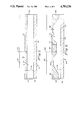
- FIG. 1 is a cross sectional representation of a waveguide in accordance with the present invention.
- FIG. 2 is a cross sectional representation of another waveguide depicting another aspect of the present invention.
- FIG. 3 is a curve of optical absorption data of TCDU (bis-phenylurethane of 5,7-dodecadiyne-1,12-diol) monomer films polymerized by ion beams in accordance with the present invention.
- TCDU bis-phenylurethane of 5,7-dodecadiyne-1,12-diol
- FIG. 4 is a curve of the absorbance of monomer films polymerized by ion beams of boron, phosphorus and arsenic at various energies of implantation versus the calculated penetration depth of these ions in accordance with the present invention.
- an optical waveguide 10 has a substrate 20, a unitary organic film 30 which has a thickness 40, a first surface 50, a second surface 60, a first region 70 comprising an organic polymer such as polydiacetylene, a second region 80 comprising a monomer of the polymer of first region 70, such as a diacetylene monomer.
- a medium 90 such as a gas, vacuum, or a coating of a material which has an index of refraction less than the first index of refraction of first region 70 and is in contact with the first surface 50 of unitary organic film 30.
- the thickness 45 of the first region can be varied by controlling the ion mass and the accelerating voltage (energy) of an ion beam 95 which is used to polymerize the unitary organic film 30 to a predetermined depth to form first region 70 leaving the second region 80 unpolymerized.
- Optical waveguide 10 is made by depositing an organic film such as a diacetylene monomer on substrate 20 forming diacetylene monomer film having a thickness 40 of about one to about 10 microns.
- the diacetylene monomer is polymerized to a predetermined depth 45 by the ion beam 95 bombardment at the surface 50.
- the depth of polymerization is controlled by the ion mass and beam energy applied to the surface 50 of the deposited film as discussed in Example 1.
- the controlled polymerization to a given depth forms first region 70 of the unitary organic film 30.
- the remaining unpolymerized monomer forms second region 80 of unitary organic film 30.
- the diacetylene monomer second region 80 corresponds to a cladding substrate and the polydiacetylene first region 70 corresponds to the core of a waveguide and their indices of refraction satisfy the requisite relationship for a waveguide in which the index of refraction of the core (first region 70) is greater than the index of refraction of the cladding substrate (second region 80) and the index of refraction of the medium 90. Furthermore, the index profile obtained in case of ion beam induced polymerization would be much closer to the uniform waveguide profile (steplike interface) when compared to diffused waveguides (exponential depth profile).
- patterning exposure to the ion beam of only a certain region of the sample in planar dimensions
- patterning can be easily utilized during the ion beam induced process of polymerization leading to the possibility of channel waveguide formation and fabrication of structures of interest such as gratings and Y-couplers.
- an optical waveguide 100 has a substrate 110, a unitary organic film 120 which has a thickness 30, a first surface 140, a second surface 150, a first region 160, and a second region 170.
- a medium 180 which has an index of refraction less than the index of refraction of the first region 160 is in contact with the first surface 140 of the unitary organic film 120.
- the thickness of the polydiacetylene first region 160 can be varied at predetermined locations by varying the mass and energy of ion beam 190.
- the ion beam 190 polymerizes the diacetylene monomer of the unitary organic film 120 to a polydiacetylene polymer to form first region 160 of unitary organic film 120 at a controlled depth.
- EXAMPLE 1 Ion beam induced polymerization of thin film TCDU (bis-phenylurethane of 5,7-dodecadiyne-1,12-diol) monomers using 150 keV arsenic and phosphorus ion beams at fluence of 1 ⁇ 10 12 cm -2
- Refractive index measurements of thin TCDU films polymerized by ion beams are greatly complicated. At the same time these measurements are performed (relatively easy) on bulk TCDU-PDA's polymerized by high energy gamma-irradiation.
- the measurements of the refractive index show that the value of n.sub. ⁇ (parallel to the chain direction) for TCDU-PDA measured at 6328 ⁇ is approximately n.sub. ⁇ ⁇ 2.2, whereas, as it is known, the refractive index for TCDU monomer is approximately 1.65, thus criterion relating to refractive indicies for propagation of a guided mode can be satisfied by ion beam induced formation of thin film polymer on a parent monomer substrate.
- FIG. 3 Optical absorption data of TCDU monomer films polymerized by ion beams at conditions mentioned above are shown in the FIG. 3.
- the baseline for each spectrum is arbitrarily shifted.
- the relative intensities are truly represented in FIG. 3. From FIG. 3 it is clearly seen that larger optical absorption correspond to higher energies of irradiation. This is due to the fact that thicker layer of monomer is polymerized by higher energy ion beam resulting in more absorption. This demonstrates that the thickness of the polymerized layer can be controlled by the parameters of implantation.
- FIG. 4 shows the dependence of absorbance (at ⁇ ⁇ 605nm) of monomer films polymerized by ion beams of boron, phosphorus and arsenic at various energies of implantation vs.
- the penetration depth of these ions calculated from LSS theory based on the density of TCDU ⁇ 1.4 gm/cm 3 .
- the absorbance depends linearly on penetration depth R p up to R p ⁇ 2000 ⁇ .
- Absorption coefficient ⁇ can be easily obtained from the linear part of FIG. 4 and is equal to ⁇ 1.2 ⁇ 10 5 cm -2 which is a typical number for polydiacetylenes.
- the nonlinearity observed at deeper penetration depth of ions suggests that a calibration has to be one before the thickness of polymerized layers can be predicted for thicker polymerization layers.
- the waveguides of the present invention and the methods for making them provide a unique product which precludes any chance of contamination of the interface of the core region (first region) and the cladding substrate region (second region). It also provides for a more uniform waveguide profile (step like interface) when compared to diffused waveguides (exponential depth profile). In addition the flexibility of the process to be able to make cores (first regions) having varied thicknesses is a decided advantage.
Landscapes
- Physics & Mathematics (AREA)
- Engineering & Computer Science (AREA)
- Microelectronics & Electronic Packaging (AREA)
- General Physics & Mathematics (AREA)
- Optics & Photonics (AREA)
- Optical Integrated Circuits (AREA)
Priority Applications (2)
| Application Number | Priority Date | Filing Date | Title |
|---|---|---|---|
| US06/852,864 US4783136A (en) | 1986-04-16 | 1986-04-16 | Optical waveguides and methods for making same |
| EP87103411A EP0241703A3 (fr) | 1986-04-16 | 1987-03-10 | Guide d'ondes optiques et son procédé de fabrication |
Applications Claiming Priority (1)
| Application Number | Priority Date | Filing Date | Title |
|---|---|---|---|
| US06/852,864 US4783136A (en) | 1986-04-16 | 1986-04-16 | Optical waveguides and methods for making same |
Publications (1)
| Publication Number | Publication Date |
|---|---|
| US4783136A true US4783136A (en) | 1988-11-08 |
Family
ID=25314433
Family Applications (1)
| Application Number | Title | Priority Date | Filing Date |
|---|---|---|---|
| US06/852,864 Expired - Fee Related US4783136A (en) | 1986-04-16 | 1986-04-16 | Optical waveguides and methods for making same |
Country Status (2)
| Country | Link |
|---|---|
| US (1) | US4783136A (fr) |
| EP (1) | EP0241703A3 (fr) |
Cited By (11)
| Publication number | Priority date | Publication date | Assignee | Title |
|---|---|---|---|---|
| US4863763A (en) * | 1987-07-13 | 1989-09-05 | Mitsubishi Petrochemical Co., Ltd. | Process for producing molecular orientated film |
| US4997244A (en) * | 1988-12-08 | 1991-03-05 | Sanyo Electric Co., Ltd. | Optical wavelength converting device and manufacturing method thereof |
| US5046801A (en) * | 1989-09-27 | 1991-09-10 | Sumitomo Metal Mining Company Limited | Optical waveguide having low optical damage |
| US5432881A (en) * | 1993-02-09 | 1995-07-11 | Nikon Corporation | Optical waveguide with overlapping diffusion regions containing different diffusion materials |
| US5462700A (en) * | 1993-11-08 | 1995-10-31 | Alliedsignal Inc. | Process for making an array of tapered photopolymerized waveguides |
| US5481385A (en) * | 1993-07-01 | 1996-01-02 | Alliedsignal Inc. | Direct view display device with array of tapered waveguide on viewer side |
| US5818983A (en) * | 1992-03-06 | 1998-10-06 | Fujitsu Limited | Optical integrated circuit, optical circuit waveguide device and process for oriented, selective growth and formation of organic film |
| US5889911A (en) * | 1993-09-28 | 1999-03-30 | Corning, Inc. U.S.A. | Precision machined warped waveguide wafer |
| US5917980A (en) * | 1992-03-06 | 1999-06-29 | Fujitsu Limited | Optical circuit device, its manufacturing process and a multilayer optical circuit using said optical circuit device |
| US6037105A (en) * | 1997-03-12 | 2000-03-14 | Samsung Electronics Co., Ltd. | Optical waveguide device fabricating method |
| US20020186950A1 (en) * | 2001-05-10 | 2002-12-12 | Tony Mule' | Optical waveguides formed from nano air-gap inter-layer dielectric materials and methods of fabrication thereof |
Families Citing this family (1)
| Publication number | Priority date | Publication date | Assignee | Title |
|---|---|---|---|---|
| GB2222272A (en) * | 1988-08-25 | 1990-02-28 | Plessey Co Plc | Organic optical waveguides of doped optically nonlinear polymer |
Citations (9)
| Publication number | Priority date | Publication date | Assignee | Title |
|---|---|---|---|---|
| US4220747A (en) * | 1976-06-28 | 1980-09-02 | Allied Chemical Corporation | Crystalline diacetylene polymers |
| US4431263A (en) * | 1979-06-25 | 1984-02-14 | University Patents, Inc. | Novel nonlinear optical materials and processes employing diacetylenes |
| US4465336A (en) * | 1980-12-16 | 1984-08-14 | Licentia Patent-Verwaltungs-Gmbh | Waveguide and method of manufacturing same |
| US4497535A (en) * | 1982-03-19 | 1985-02-05 | Gte Laboratories Incorporated | Optical pulse generator |
| US4515429A (en) * | 1980-05-27 | 1985-05-07 | At&T Bell Laboratories | Nonlinear and bistable optical waveguide devices |
| US4531809A (en) * | 1983-09-08 | 1985-07-30 | Gte Laboratories Incorporated | Optical waveguide coupling device |
| US4536450A (en) * | 1980-03-12 | 1985-08-20 | University Patents, Inc. | Nonlinear optical materials and processes employing diacetylenes |
| US4615962A (en) * | 1979-06-25 | 1986-10-07 | University Patents, Inc. | Diacetylenes having liquid crystal phases |
| US4691982A (en) * | 1984-03-10 | 1987-09-08 | Canon Kabushiki Kaisha | Optical coupler |
Family Cites Families (2)
| Publication number | Priority date | Publication date | Assignee | Title |
|---|---|---|---|---|
| JPS547948A (en) * | 1977-06-21 | 1979-01-20 | Nippon Telegr & Teleph Corp <Ntt> | Optical circuit of high molecule |
| FR2426922A1 (fr) * | 1978-05-26 | 1979-12-21 | Thomson Csf | Structure optique compacte a source integree |
-
1986
- 1986-04-16 US US06/852,864 patent/US4783136A/en not_active Expired - Fee Related
-
1987
- 1987-03-10 EP EP87103411A patent/EP0241703A3/fr not_active Withdrawn
Patent Citations (9)
| Publication number | Priority date | Publication date | Assignee | Title |
|---|---|---|---|---|
| US4220747A (en) * | 1976-06-28 | 1980-09-02 | Allied Chemical Corporation | Crystalline diacetylene polymers |
| US4431263A (en) * | 1979-06-25 | 1984-02-14 | University Patents, Inc. | Novel nonlinear optical materials and processes employing diacetylenes |
| US4615962A (en) * | 1979-06-25 | 1986-10-07 | University Patents, Inc. | Diacetylenes having liquid crystal phases |
| US4536450A (en) * | 1980-03-12 | 1985-08-20 | University Patents, Inc. | Nonlinear optical materials and processes employing diacetylenes |
| US4515429A (en) * | 1980-05-27 | 1985-05-07 | At&T Bell Laboratories | Nonlinear and bistable optical waveguide devices |
| US4465336A (en) * | 1980-12-16 | 1984-08-14 | Licentia Patent-Verwaltungs-Gmbh | Waveguide and method of manufacturing same |
| US4497535A (en) * | 1982-03-19 | 1985-02-05 | Gte Laboratories Incorporated | Optical pulse generator |
| US4531809A (en) * | 1983-09-08 | 1985-07-30 | Gte Laboratories Incorporated | Optical waveguide coupling device |
| US4691982A (en) * | 1984-03-10 | 1987-09-08 | Canon Kabushiki Kaisha | Optical coupler |
Cited By (13)
| Publication number | Priority date | Publication date | Assignee | Title |
|---|---|---|---|---|
| US4863763A (en) * | 1987-07-13 | 1989-09-05 | Mitsubishi Petrochemical Co., Ltd. | Process for producing molecular orientated film |
| US4997244A (en) * | 1988-12-08 | 1991-03-05 | Sanyo Electric Co., Ltd. | Optical wavelength converting device and manufacturing method thereof |
| US5046801A (en) * | 1989-09-27 | 1991-09-10 | Sumitomo Metal Mining Company Limited | Optical waveguide having low optical damage |
| US5818983A (en) * | 1992-03-06 | 1998-10-06 | Fujitsu Limited | Optical integrated circuit, optical circuit waveguide device and process for oriented, selective growth and formation of organic film |
| US6338975B1 (en) | 1992-03-06 | 2002-01-15 | Fujitsu Limited | Optical circuit device, its manufacturing process and a multilayer optical circuit using said optical circuit device |
| US5917980A (en) * | 1992-03-06 | 1999-06-29 | Fujitsu Limited | Optical circuit device, its manufacturing process and a multilayer optical circuit using said optical circuit device |
| US5432881A (en) * | 1993-02-09 | 1995-07-11 | Nikon Corporation | Optical waveguide with overlapping diffusion regions containing different diffusion materials |
| US5481385A (en) * | 1993-07-01 | 1996-01-02 | Alliedsignal Inc. | Direct view display device with array of tapered waveguide on viewer side |
| US5889911A (en) * | 1993-09-28 | 1999-03-30 | Corning, Inc. U.S.A. | Precision machined warped waveguide wafer |
| US5462700A (en) * | 1993-11-08 | 1995-10-31 | Alliedsignal Inc. | Process for making an array of tapered photopolymerized waveguides |
| US6037105A (en) * | 1997-03-12 | 2000-03-14 | Samsung Electronics Co., Ltd. | Optical waveguide device fabricating method |
| US20020186950A1 (en) * | 2001-05-10 | 2002-12-12 | Tony Mule' | Optical waveguides formed from nano air-gap inter-layer dielectric materials and methods of fabrication thereof |
| US6947651B2 (en) | 2001-05-10 | 2005-09-20 | Georgia Tech Research Corporation | Optical waveguides formed from nano air-gap inter-layer dielectric materials and methods of fabrication thereof |
Also Published As
| Publication number | Publication date |
|---|---|
| EP0241703A3 (fr) | 1987-12-23 |
| EP0241703A2 (fr) | 1987-10-21 |
Similar Documents
| Publication | Publication Date | Title |
|---|---|---|
| US4783136A (en) | Optical waveguides and methods for making same | |
| Kokubun et al. | Athermal waveguides for temperature-independent lightwave devices | |
| Carter et al. | Intensity‐dependent index of refraction in multilayers of polydiacetylene | |
| US5932397A (en) | Multicolor lithography for control of three dimensional refractive index gradient processing | |
| Rochon et al. | Guided mode resonance filters using polymer films | |
| WO1991010149A1 (fr) | Procede de formation de guides d'ondes optiquement actifs | |
| US20030081876A1 (en) | Tuning of optical waveguide devices containing an organic material | |
| Darraud et al. | Optical modifications of polymers by ion beam irradiation | |
| Beyer et al. | Holographic recording of Bragg gratings for wavelength division multiplexing in doped and partially polymerized poly (methyl methacrylate) | |
| Glavas et al. | Thermal stability of ion implanted LiTaO3 and LiNbO3 optical waveguides | |
| Bentini et al. | Integrated Mach-Zehnder micro-interferometer on LiNbO3 | |
| Zou et al. | Tunable planar polymer Bragg gratings having exceptionally low polarization sensitivity | |
| Schlotter et al. | Fabrication of channel waveguides in polydiacetylenes: Composite diffused glass/polymer structures | |
| Kulish et al. | Ion implantation, a method for fabricating light guides in polymers | |
| Weber et al. | Organic materials for integrated optics | |
| Chen et al. | Optical interconnection using polymer microstructure waveguides | |
| Frank et al. | Ionizing radiation for fabrication of optical waveguides in polymers | |
| Brunner et al. | Polymer based waveguiding structures obtained by ion beam irradiation at different energies | |
| AU716343B2 (en) | Manufacture of planar waveguide and planar waveguide | |
| Palchetti et al. | Photobleaching of polydiacetylene waveguides: a characterization of the process and patterning of optical elements | |
| Gong et al. | Efficient grating coupling to poly-4BCMU optical waveguides | |
| Diemeer et al. | Low-loss nonlinear optical polymeric waveguide materials and devices | |
| Liu et al. | Tailoring the transmission characteristics of polymer long-period waveguide gratings by UV irradiation | |
| Kulisch et al. | Fabrication of lightguides in in-diffused bulk PMMA | |
| CA2396505A1 (fr) | Accord de guides d'ondes optiques contenant un materiau organique |
Legal Events
| Date | Code | Title | Description |
|---|---|---|---|
| AS | Assignment |
Owner name: GTE LABORATORIES INCORPORATED, A CORP OF DE. Free format text: ASSIGNMENT OF ASSIGNORS INTEREST.;ASSIGNORS:ELMAN, BORIS S.;THAKUR, MRINAL K.;SEYMOUR, ROBERT J.;REEL/FRAME:004551/0088 Effective date: 19860411 Owner name: GTE LABORATORIES INCORPORATED, ARIZONA Free format text: ASSIGNMENT OF ASSIGNORS INTEREST;ASSIGNORS:ELMAN, BORIS S.;THAKUR, MRINAL K.;SEYMOUR, ROBERT J.;REEL/FRAME:004551/0088 Effective date: 19860411 |
|
| FEPP | Fee payment procedure |
Free format text: PAYOR NUMBER ASSIGNED (ORIGINAL EVENT CODE: ASPN); ENTITY STATUS OF PATENT OWNER: LARGE ENTITY |
|
| FEPP | Fee payment procedure |
Free format text: PAYER NUMBER DE-ASSIGNED (ORIGINAL EVENT CODE: RMPN); ENTITY STATUS OF PATENT OWNER: LARGE ENTITY Free format text: PAYOR NUMBER ASSIGNED (ORIGINAL EVENT CODE: ASPN); ENTITY STATUS OF PATENT OWNER: LARGE ENTITY |
|
| FPAY | Fee payment |
Year of fee payment: 4 |
|
| REMI | Maintenance fee reminder mailed | ||
| LAPS | Lapse for failure to pay maintenance fees | ||
| FP | Lapsed due to failure to pay maintenance fee |
Effective date: 19961113 |
|
| STCH | Information on status: patent discontinuation |
Free format text: PATENT EXPIRED DUE TO NONPAYMENT OF MAINTENANCE FEES UNDER 37 CFR 1.362 |