US4815823A - Electro-optical device with plural low resistive portions on each high resistive electrode - Google Patents
Electro-optical device with plural low resistive portions on each high resistive electrode Download PDFInfo
- Publication number
- US4815823A US4815823A US07/148,753 US14875388A US4815823A US 4815823 A US4815823 A US 4815823A US 14875388 A US14875388 A US 14875388A US 4815823 A US4815823 A US 4815823A
- Authority
- US
- United States
- Prior art keywords
- conductor film
- optical modulation
- resistivity
- liquid crystal
- substrate
- Prior art date
- Legal status (The legal status is an assumption and is not a legal conclusion. Google has not performed a legal analysis and makes no representation as to the accuracy of the status listed.)
- Expired - Lifetime
Links
Images


Classifications
-
- G—PHYSICS
- G09—EDUCATION; CRYPTOGRAPHY; DISPLAY; ADVERTISING; SEALS
- G09G—ARRANGEMENTS OR CIRCUITS FOR CONTROL OF INDICATING DEVICES USING STATIC MEANS TO PRESENT VARIABLE INFORMATION
- G09G3/00—Control arrangements or circuits, of interest only in connection with visual indicators other than cathode-ray tubes
- G09G3/20—Control arrangements or circuits, of interest only in connection with visual indicators other than cathode-ray tubes for presentation of an assembly of a number of characters, e.g. a page, by composing the assembly by combination of individual elements arranged in a matrix no fixed position being assigned to or needed to be assigned to the individual characters or partial characters
- G09G3/34—Control arrangements or circuits, of interest only in connection with visual indicators other than cathode-ray tubes for presentation of an assembly of a number of characters, e.g. a page, by composing the assembly by combination of individual elements arranged in a matrix no fixed position being assigned to or needed to be assigned to the individual characters or partial characters by control of light from an independent source
- G09G3/36—Control arrangements or circuits, of interest only in connection with visual indicators other than cathode-ray tubes for presentation of an assembly of a number of characters, e.g. a page, by composing the assembly by combination of individual elements arranged in a matrix no fixed position being assigned to or needed to be assigned to the individual characters or partial characters by control of light from an independent source using liquid crystals
- G09G3/3611—Control of matrices with row and column drivers
- G09G3/3622—Control of matrices with row and column drivers using a passive matrix
- G09G3/3629—Control of matrices with row and column drivers using a passive matrix using liquid crystals having memory effects, e.g. ferroelectric liquid crystals
- G09G3/3637—Control of matrices with row and column drivers using a passive matrix using liquid crystals having memory effects, e.g. ferroelectric liquid crystals with intermediate tones displayed by domain size control
-
- G—PHYSICS
- G02—OPTICS
- G02F—OPTICAL DEVICES OR ARRANGEMENTS FOR THE CONTROL OF LIGHT BY MODIFICATION OF THE OPTICAL PROPERTIES OF THE MEDIA OF THE ELEMENTS INVOLVED THEREIN; NON-LINEAR OPTICS; FREQUENCY-CHANGING OF LIGHT; OPTICAL LOGIC ELEMENTS; OPTICAL ANALOGUE/DIGITAL CONVERTERS
- G02F1/00—Devices or arrangements for the control of the intensity, colour, phase, polarisation or direction of light arriving from an independent light source, e.g. switching, gating or modulating; Non-linear optics
- G02F1/01—Devices or arrangements for the control of the intensity, colour, phase, polarisation or direction of light arriving from an independent light source, e.g. switching, gating or modulating; Non-linear optics for the control of the intensity, phase, polarisation or colour
- G02F1/13—Devices or arrangements for the control of the intensity, colour, phase, polarisation or direction of light arriving from an independent light source, e.g. switching, gating or modulating; Non-linear optics for the control of the intensity, phase, polarisation or colour based on liquid crystals, e.g. single liquid crystal display cells
- G02F1/133—Constructional arrangements; Operation of liquid crystal cells; Circuit arrangements
- G02F1/1333—Constructional arrangements; Manufacturing methods
- G02F1/1343—Electrodes
- G02F1/134309—Electrodes characterised by their geometrical arrangement
- G02F1/134336—Matrix
-
- G—PHYSICS
- G02—OPTICS
- G02F—OPTICAL DEVICES OR ARRANGEMENTS FOR THE CONTROL OF LIGHT BY MODIFICATION OF THE OPTICAL PROPERTIES OF THE MEDIA OF THE ELEMENTS INVOLVED THEREIN; NON-LINEAR OPTICS; FREQUENCY-CHANGING OF LIGHT; OPTICAL LOGIC ELEMENTS; OPTICAL ANALOGUE/DIGITAL CONVERTERS
- G02F1/00—Devices or arrangements for the control of the intensity, colour, phase, polarisation or direction of light arriving from an independent light source, e.g. switching, gating or modulating; Non-linear optics
- G02F1/01—Devices or arrangements for the control of the intensity, colour, phase, polarisation or direction of light arriving from an independent light source, e.g. switching, gating or modulating; Non-linear optics for the control of the intensity, phase, polarisation or colour
- G02F1/13—Devices or arrangements for the control of the intensity, colour, phase, polarisation or direction of light arriving from an independent light source, e.g. switching, gating or modulating; Non-linear optics for the control of the intensity, phase, polarisation or colour based on liquid crystals, e.g. single liquid crystal display cells
- G02F1/133—Constructional arrangements; Operation of liquid crystal cells; Circuit arrangements
- G02F1/1333—Constructional arrangements; Manufacturing methods
- G02F1/1345—Conductors connecting electrodes to cell terminals
-
- G—PHYSICS
- G09—EDUCATION; CRYPTOGRAPHY; DISPLAY; ADVERTISING; SEALS
- G09G—ARRANGEMENTS OR CIRCUITS FOR CONTROL OF INDICATING DEVICES USING STATIC MEANS TO PRESENT VARIABLE INFORMATION
- G09G2310/00—Command of the display device
- G09G2310/06—Details of flat display driving waveforms
- G09G2310/066—Waveforms comprising a gently increasing or decreasing portion, e.g. ramp
-
- G—PHYSICS
- G09—EDUCATION; CRYPTOGRAPHY; DISPLAY; ADVERTISING; SEALS
- G09G—ARRANGEMENTS OR CIRCUITS FOR CONTROL OF INDICATING DEVICES USING STATIC MEANS TO PRESENT VARIABLE INFORMATION
- G09G2380/00—Specific applications
- G09G2380/04—Electronic labels
-
- G—PHYSICS
- G09—EDUCATION; CRYPTOGRAPHY; DISPLAY; ADVERTISING; SEALS
- G09G—ARRANGEMENTS OR CIRCUITS FOR CONTROL OF INDICATING DEVICES USING STATIC MEANS TO PRESENT VARIABLE INFORMATION
- G09G3/00—Control arrangements or circuits, of interest only in connection with visual indicators other than cathode-ray tubes
- G09G3/20—Control arrangements or circuits, of interest only in connection with visual indicators other than cathode-ray tubes for presentation of an assembly of a number of characters, e.g. a page, by composing the assembly by combination of individual elements arranged in a matrix no fixed position being assigned to or needed to be assigned to the individual characters or partial characters
- G09G3/2007—Display of intermediate tones
- G09G3/2011—Display of intermediate tones by amplitude modulation
-
- G—PHYSICS
- G09—EDUCATION; CRYPTOGRAPHY; DISPLAY; ADVERTISING; SEALS
- G09G—ARRANGEMENTS OR CIRCUITS FOR CONTROL OF INDICATING DEVICES USING STATIC MEANS TO PRESENT VARIABLE INFORMATION
- G09G3/00—Control arrangements or circuits, of interest only in connection with visual indicators other than cathode-ray tubes
- G09G3/20—Control arrangements or circuits, of interest only in connection with visual indicators other than cathode-ray tubes for presentation of an assembly of a number of characters, e.g. a page, by composing the assembly by combination of individual elements arranged in a matrix no fixed position being assigned to or needed to be assigned to the individual characters or partial characters
- G09G3/2007—Display of intermediate tones
- G09G3/2014—Display of intermediate tones by modulation of the duration of a single pulse during which the logic level remains constant
-
- G—PHYSICS
- G09—EDUCATION; CRYPTOGRAPHY; DISPLAY; ADVERTISING; SEALS
- G09G—ARRANGEMENTS OR CIRCUITS FOR CONTROL OF INDICATING DEVICES USING STATIC MEANS TO PRESENT VARIABLE INFORMATION
- G09G3/00—Control arrangements or circuits, of interest only in connection with visual indicators other than cathode-ray tubes
- G09G3/20—Control arrangements or circuits, of interest only in connection with visual indicators other than cathode-ray tubes for presentation of an assembly of a number of characters, e.g. a page, by composing the assembly by combination of individual elements arranged in a matrix no fixed position being assigned to or needed to be assigned to the individual characters or partial characters
- G09G3/2007—Display of intermediate tones
- G09G3/207—Display of intermediate tones by domain size control
Definitions
- the present invention relates to an optical modulation device for a display panel, more particularly to a liquid crystal optical modulation device adapted to gradational or tonal display for a display panel, such as a display, a shutter array, etc., using a ferroelectric liquid crystal.
- bistable liquid crystals ferroelectric liquid crystals showing chiral smectic C phase (SmC*) or H phase (SmH*) are generally used.
- liquid crystal materials have bistability, i.e., a property of assuming either a first stable state or a second stable state and retaining the resultant state when the electric field is not applied, and has a high response speed in response to a change in electric field, so that they are expected to be widely used in the field of a high speed and memory type display apparatus, etc.
- this bistable liquid crystal device may still involve a problem that the switching between the first and second stable states is so fast that it is difficult to control an intermediate level between the two stable states. For this reason, it has been difficult to display an intermediate gradation.
- our research group has already proposed a novel optical modulation device solving the above problems by using an optical modulation material having a memory characteristic such as a ferroelectric liquid crystal as described above (U.S. patent applications Ser. Nos. 931,082 and 934,920).
- optical modulation device can have a large pixel capacity and effect a gradational display.
- the optical modulation device still involves several problems in respects of actual production and operation, such as a large number of electrodes, complicated connection with wires from a driving power supply and electrodes on substrates and fluctuation in display performances due to generation of Joule's heat by a current passing between the electrodes and change in potential gradient.
- a principal object of the present invention is to provide an optical modulation device which can be produced easily and capable of providing a stable gradational display with high-density pixels.
- an optical modulation device comprising: a first substrate having thereon a high-resistivity transparent conductor film and a plurality of low-resistivity conductor films disposed on the transparent conductor film and dividing the transparent conductor film into plural stripes; a second substrate having thereon a plurality of transparent conductor film stripes; and an optical modulation material interposed between the first and second substrates;
- said optical modulation device further includes a plurality of connecting conductors for connection with an external driver, the connecting conductors being disposed in a region free of the high-resistivity transparent conductor film of the first substrate and each connected to one of the low-resistivity conductor films.
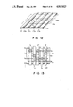
- FIGS. 1A and 1B are a plan view and a sectional view showing an electrode structure on a substrate
- FIG. 2 is an enlarged partial view of the side portions of a substrate
- FIGS. 3 and 12 are partial perspective views showing a substrate structure
- FIGS. 4A and 4B are explanatory views schematically showing a potential gradient
- FIG. 5 is a schematic view for illustrating electric signals
- FIG. 6, FIGS. 7A-7E, FIGS. 9A-9E, FIG. 10 and FIGS. 11A-11E are explanatory views showing pulse waveforms
- FIGS. 8A-8D are schematic views showing gradational display states of a pixel
- FIG. 13 is an explanatory view schematically showing a display state of a picture
- FIG. 14 is a schematic plan view showing another electrode structure.
- FIGS. 15 and 16 are schematic views for explaining an operation principle of a ferroelectric liquid crystal cell.
- FIG. 3 is a partial perspective view of a substrate for a liquid crystal optical device constituting an embodiment of the optical modulation device according to the present invention.
- the other substrate Opposite the substrate 1, the other substrate (not shown) is disposed having a counter conductor film (counter electrode) 4 thereon so as to intersect with the transmission electrodes 3 to define pixels, e.g., one denoted by A.
- the above mentioned optical modulation material is sandwiched between the display conductor film 2 and the counter electrode 4.
- a potential gradient may be provided along the conductor film by applying a scanning voltage to a transmission electrode 3, thereby to cause a voltage gradient in electric field between the display conductor film 2 and a counter electrode 4.
- a transmission electrode 3b for example, is supplied with a prescribed signal voltage Va and adjacent transmission electrodes 3a and 3c are supplied with a reference potential V E (e.g., 0 volt), a potential gradient of Va is provided in a length L 1 between the transmission electrodes 3b and 3a and in a length L 2 between 3b and 3c along the extension of the conductor film 2.
- V E reference potential
- the inversion threshold voltage Vth is assumed to be Va, and a signal of -Vb is applied to the counter electrode 4, a potential difference Va+Vb exceeding the inversion threshold voltage Vth is applied to the ferroelectric liquid crystal corresponding to lengths m 1 and m 2 along the extension of the conductor film 32, so that the region corresponding to the m 1 +m 2 may be inverted, e.g., from the bright state to the dark state.
- a gradation may be displayed by applying a value Vb of signal selected corresponding to given gradation data to individual pixels.
- Vb of signal selected corresponding to given gradation data
- a 2000 ⁇ -thick transparent conductor film of SnO 2 (tin oxide) is formed by sputtering as a conductor film 2 on a glass substrate 1.
- a 1000 ⁇ -thick Al film is formed by vacuum evaporation on the Sn 2 film and then patterned to form a plurality of transmission electrodes 3 in the form of stripes.
- a uniform Al film may be formed by vacuum evaporation and then patterned to easily form a plurality of the transmission electrodes 3.
- the transmission electrodes may be formed with a spacing of 230 ⁇ m and a width of 20 ⁇ m.
- the above-described method it is possible to omit a step for fine etching of the SnO 2 film and further a step for fine etching of the conductor film such as an ITO film.
- a step for fine etching of the SnO 2 film it is also possible to form a fine pattern of SnO 2 film or ITO film as desired.
- BF 3 boron trifluoride
- counter electrodes 4 of ITO (indium tin oxide) film may be formed on a counter substrate by sputtering.
- an about 500 ⁇ -thick polyvinyl alcohol film is formed as a liquid crystal alignment film and subjected to a rubbing treatment.
- a counter substrate is provided, an alignment film is formed, and an aligning treatment such as rubbing is effected.
- the sheet resistivity (according to ASTM D 257) of the display conductor film 32 may preferably be on the order of 10 4 ⁇ / ⁇ (ohm per square) -10 7 106 / ⁇ and may be on the order of 10 3 -10 9 ⁇ / ⁇ as a tolerable range.
- An example of a film having such a resistivity may be an SnO 2 film as described above formed by sputtering in an argon stream containing oxygen. Such a method of sputtering in an argon stream is disclosed, for example, by D. B. Fraser and H. D. Cook, "Highly Conductive Transparent Films of Sputtered In 2 -xSn x 0 3- y", Journal of the Electrochemical Society Solid-State Science and Technology, Vol. 119, No. 10 (published in 1972).
- the above described gradational display may be applicable to a wide variety of optical modulation materials, and moreover the power consumption can be minimized when a potential gradient is provided in the above mentioned manner.
- the above condition is first of all effective to suppress the heat generation due to a current passing through the display electrode at the time of forming a potential gradient for gradational display.
- the temperature increase ⁇ T of the electrode may be calculated by the following equation as a simple theoretical calculation where a heat dissipation to the glass substrate, etc., is not considered: ##EQU1## wherein the respective symbols denote the following: V: Va-VE (potential difference between transmission electrodes),
- ⁇ T is calculated to be on the order of 250000/R (°K.). Even if the heat dissipation or conduction to the glass substrate, etc., is considered here, if the R (equal to the sheet resistivity as described above) is on the order of several ⁇ to several tens of ⁇ , the temperature increase amounts to a considerable value. It is possible that the temperature increase exerts an ill effect on the .
- the effect is further pronounced when the voltage is increased, the writing period for a pixel in increased, or even if the writing period becomes shorter, the pixel area is decreased further.
- the voltage V is 10 volts
- the power consumption per pixel becomes 1 W, which amounts to a large value of 1 KW when a large number of such pixels are arranged in a matrix and, e.g., 1000 pixels are provided with a gradation at a time.
- the sheet resistivity of 10 4 ⁇ / ⁇ or more may preferably be selected.
- the upper limit of the sheet resistivity may preferably be on the order of 10 9 ⁇ / ⁇ or below, further preferably on the order of 10 7 ⁇ / ⁇ or below.
- the reason for this may be considered as follows. If the dielectric constant of an optical modulation material used is assumed to be about 5, a typical value for a ferroelectric liquid crystal, the layer thickness thereof be 1 ⁇ m, and the pixel area be 230 ⁇ m square, then the capacitance of the liquid crystal layer becomes about 2.5 pF (2.5 ⁇ 10 -12 F) per pixel.
- FIGS. 1A (plan view) and 1B (sectional view) show a structure or arrangement of electrodes on a substrate.
- transmission electrodes 3 are disposed in parallel with each other and with equal spacings on a high-resistivity transparent conductor film 2, whereby a resistive film region 5 is formed. Every other transmission electrode 3 extends its end so as to form an electrode extension 6.
- the electrode extension 6 is formed integrally with a transmission electrode 3 and on the same substrate as the transmission electrode 3 and is connected to a connector 7 for connection with wires from an external drive (not shown).
- the connector 7 has connecting conductors 8 to which driving voltages are supplied from the external driver through cables 9b formed on a flexible substrate 9a.
- FIG. 2 is an enlarged view of the side portions of the substrate shown in FIG. 1A.
- the width of a connecting conductor 8 of the connector 7 can be enlarged, whereby the difficulty in providing the substrate 1 with the connector is remarkably alleviated.
- a spacing or gap b between connecting conductors 8a and 8b adjacent to each other is free of a resistive film (extended portion of the high-resistivity conductor film 2), so that the spacing b can be smaller than a spacing a between the transmission electrodes 3.
- the connection with prescribed transmission electrode can be secured because each connecting conductor may have a sufficiently large width. As a result, the efficiency of device production can be improved.
- the respective parameters shown in FIG. 2 are taken in the following ranges: a: 50-500 ⁇ m, b: 10-50 ⁇ m, 50 ⁇ m or longer, preferably 100 ⁇ m or longer; d (distance between the high-resistivity conductor film 2 and a connecting conductor 8): 20 ⁇ m or longer, preferably 50 ⁇ m or longer; e (width of a transmission electrode): from 1/20 to 1/4 of a; and the difference c-d: 10 ⁇ m or longer.
- the above-described resistive film-free region, where the liquid crystals 8 are disposed, may be relatively easily formed, e.g., by masking the regions on both sides of the substrate 1 for connection with the connectors 7 when the high-resistivity transparent conductor film 2 is formed, e.g., by sputtering.
- the transmission electrodes 3 have a function of transferring a voltage from the connection to the display electrode (high-resistivity conductor film), so that those having a sufficiently low resistivity, e.g., around 1 ⁇ / ⁇ or lower may be used therefor.
- the counter electrode 4 may for example be composed of an ITO film having a sheet resistivity of around 20 ⁇ / ⁇ and may be used as described above.
- two substrates prepared in the above described manner were disposed opposite to each other with a spacing of about 1 m to form a cell, into which a ferroelectric liquid crystal (a composition consisting mainly of p-n-octyloxybenzoic acid-p'-(2-methylbutyloxy)phenylester and p-n-nonyloxybenzoic acid-p'-(2-methylbutyloxy) phenyl-ester) was injected.
- the size of the pixel A constituted by a superposed portion of a display conductor film 2 and a counter electrode 4 was made 230 ⁇ m ⁇ 230 ⁇ m, where the width of the pixel A was made L 1 /2+L 2 /2.
- FIG. 5 schematically illustrates a method of applying electric signals to a liquid crystal cell which includes a substrate 1, a display conductor film 2, transmission electrodes 3a, 3b and 3c, a counter conductor film 4 disposed or a counter substrate 10, and a ferroelectric liquid crystal 9 sandwiched between the two substrates.
- the counter conductor film 4 is connected to a first driven circuit 11, and the display conductor film 2 is connected to a second driver circuit.
- FIGS. 6 and 7 show electric signals applied to the liquid crystal cell. More specifically, FIG. 6 shows a waveform of SIGNAL(A) generated by the driver circuit 11 shown in FIG. 5, and Figures 7A-7E show waveforms of SIGNAL(B) generated by the driver circuit 12 shown in FIG. 5.
- a 200 ⁇ sec-pulse of -12 V is applied as a signal(B) to all the transmission electrodes 3a, 3b, 3c, . . . , and a 200 ⁇ sec-pulse of 8 V (called "erasure pulse”) is preliminarily applied in phase with a counter electrode 4 in an erasure step.
- the liquid crystal 9 is switched to the first stable state to provide a pixel A (FIG. 3) wholly with a bright state (as a pair of polarizers are arranged in cross nicols in such a manner).
- the liquid crystal used herein is assumed to have a switching or inversion threshold of ⁇ 15 V- ⁇ 16 V.
- optical state changes as shown in Figures 8A-8D may also be obtained when various pulses (A) with different pulse durations as shown in Figures 9A-9E are applied in phase with a triangular wave signal (B) as shown in FIG. 10. More specifically, in this instance, a gradational display may be effected by applying the signal shown in FIG. 10 to the transmission electrode 3b while applying the pulses shown in FIGS. 9A-9E to the counter electrode 4 corresponding to given gradation data in phase with the signal applied to the transmission electrode 3b.
- the signal (A) or (B) supplied from the driver circuit 11 or 12 has a high frequency of, e.g., 1 kHz or higher because the generation of Joule's heat is suppressed by using a high-frequency driving voltage.
- the transmission electrodes 3a, 3b, . . . may be composed of a metal such as silver, copper, gold or chromium, or a transparent electrode such as low-resistivity ITO instead of aluminum (Al) used in the above example.
- the sheet resistivity may preferably be 10 2 ⁇ / ⁇ or below.
- the sheet resistivity of the electrodes may be adjusted to an appropriate value, for example, by controlling the film thickness.
- FIG. 12 is a partial schematic view of a specific embodiment of a liquid crystal panel adapted to application of the gradational display system to matrix or multiplex driving.
- the display panel shown in FIG. 12 comprises a conductor film 22 disposed on a glass substrate 21, and transmission electrodes 23 (23a, 23b, 23c, . . . ) of a low-resistivity disposed on the conductor film 22.
- transmission electrodes 23 23a, 23b, 23c, . . .
- counter substrate Opposite the substrate 21, there is disposed a counter substrate (not shown) on which counter electrodes 24 (24a, 24b, . . . ) are disposed.
- a ferroelectric liquid crystal is disposed between the conductor film 22 and the counter electrodes 24.
- all the transmission electrodes 23 may be placed at the same potential level so as to apply a uniform electric field across the whole or a prescribed part of the pixels formed at the intersections of the stripe conductor films 22 and the stripe counter electrodes 24, thereby to bring the whole or the prescribed part of the pixels to either one of the bright and dark states at a time; or prior to writing for each writing line, the whole or a prescribed part of the pixels on the writing line are brought to either one of the bright and dark states. Then, a pulse as shown in FIG.
- the scanning selection signal is preferably be made a voltage pulse equal to or somewhat lower than the inversion threshold voltage of the ferroelectric liquid crystal.
- the above-mentioned scanning signal is first applied to odd-numbered terminals S 1 , S 3 , S 5 , . . . S 2n-1 sequentially and then applied to even-numbered terminals S 2 , S 4 , S 6 , . . . S 2n sequentially.
- the reference potential V E has been generally explained to be zero potential but can be raised to have a positive value.
- the difference Va-V E becomes smaller to result in a smaller potential gradient for providing a gradation, but the absolute value of an information signal can be decreased.
- optical modulation device it is also possible to effect a gradational display over the entire frame by sequentially applying a scanning signal to the abovementioned stripe counter electrodes 24, applying gradation signals to odd-numbered (or even-numbered) transmission electrodes in phase with the scanning signal while connecting the even-numbered (or odd-numbered) transmission electrodes to the reference potential point, and then applying gradation signals to even-numbered (or odd-numbered) transmission electrodes while connecting the odd-numbered (or even-numbered) transmission electrodes to the reference potential point.
- a power consumed in display electrodes between transmission electrodes for supplying information signals amounts to those required at pixels in a number of 1000 ⁇ (the number of selected pixels).
- the power consumed becomes considerable unless the display electrodes have an appropriately low resistivity. Accordingly, it is most preferable to provide a potential gradient between transmission electrodes for supplying a scanning signal.
- FIG. 14 shows another embodiment of the present invention.
- a conductor film 31 is formed on one substrate and a plurality of low-resistivity transmission electrodes 33 are formed thereon so as to define the conductor film 31 into stripes.
- a conductor film 32 is disposed opposite the conductor film 31 by the medium of a ferroelectric liquid crystal (not shown).
- a plurality of low-resistivity transmission electrodes are formed on the conductor film 32 so as to define the conductor film 32 into stripes which intersect with the stripes of the conductor film 31.
- each pixel after the erasure step can be provided with a potential gradient along the scanning signal side conductor film and a potential gradient also along the information signal side conductor film, so that potential gradients generated on both sides are applied to the ferroelectric liquid crystal in a pixel.
- a gradational display with more gradation levels can be provided.
- a material which shows a first optically stable state (e.g., assumed to form a "bright” state) and a second optically stable state (e.g., assumed to form a "dark” state) depending on an electric field applied thereto, i.e., one showing at least two stable states in response to an electric field, particularly a liquid crystal showing such a property, may be used.
- Preferable ferroelectric liquid crystals showing at least two stable states, particularly bistability, which can be used in the driving method according to the present invention are chiral smectic liquid crystals having ferroelectricity, among which liquid crystals showing chiral smectic C phase (SmC*), H phase (SmH*), I phase (SmI*), F phase (SmF*) or G phase (SmG*) are suitable.
- ferroelectric liquid crystals are described in, e.g., "LE JOURNAL DE PHYSIQUE LETTRE” 36 (L-69), 1975 "Ferroelectric Liquid Crystals”: “Applied Physics Letters” 36 (11) 1980, “Submicro Second Bistable Electrooptic Switching in Liquid Crystals”, “Kotai Butsuri (Solid State Physics)” 16 (141), 1981 “Liquid Crystal”, etc. Ferroelectric liquid crystals disclosed in these publications may be used in the present invention.
- ferroelectric liquid crystal compound usable in the method according to the present invention examples include decyloxybenzylidene-p'-amino-2-methylbutyl cinnamate (DOBAMBC), hexyloxybenzylidene-p'-amino-2-chloropropyl cinnamate (HOBACPC), 4-O-(2-methyl)-butylresorcylidene-4'-octylaniline (MBRA 8 ), etc.
- DOBAMBC decyloxybenzylidene-p'-amino-2-methylbutyl cinnamate
- HOBACPC hexyloxybenzylidene-p'-amino-2-chloropropyl cinnamate
- MBRA 8 4-O-(2-methyl)-butylresorcylidene-4'-octylaniline
- the device When a device is constituted using these materials, the device may be supported with a block of copper, etc., in which a heater is embedded in order to realize a temperature condition where the liquid crystal compounds assume an SmC*, SmH*, SmI*, SmF* or SmG* phase.
- FIG. 15 there is schematically shown an example of a ferroelectric liquid crystal cell for explanation of the operation thereof.
- Reference numerals 101a and 101b denote substrates (glass plates) on which a transparent electrode of, e.g., In 2 O 3 , SnO 2 , ITO (Intium-Tin-Oxide), etc., is disposed, respectively.
- a liquid crystal of, e.g., an SmC*-phase in which liquid crystal molecular layers 102 are oriented perpendicular to surfaces of the glass plates is hermetically disposed therebetween.
- Full lines 103 show liquid crystal molecules.
- Each liquid crystal molecule 103 has a dipole moment (P.sub. ⁇ ) 104 in a direction perpendicular to the axis thereof.
- liquid crystal molecules 103 When a voltage higher than a certain threshold level is applied between electrodes formed on the base plates 101a and 101b, a helical structure of the liquid crystal molecule 103 is unwound or released to change the alignment direction of respective liquid crystal molecules 103 so that the dipole moment (P.sub. ⁇ ) 104 are all directed in the direction of the electric field.
- the liquid crystal molecules 103 have an elongated shape and show refractive anisotropy between the long axis and the short axis thereof.
- the liquid crystal cell when, for instance, polarizers arranged in a cross nicol relationship, i.e., with their polarizing directions crossing each other, are disposed on the upper and the lower surfaces of the glass plates, the liquid crystal cell thus arranged functions as a liquid crystal optical modulation device, of which optical characteristics vary depending upon the polarity of an applied voltage.
- the helical structure of the liquid crystal molecules is unwound to provide a non-helical structure even in the absence of an electric field whereby the dipole moment assumes either of the two states, i.e., Pa in an upper direction 114a or Pb in a lower direction 114b as shown in FIG. 16.
- electric field Ea or Eb higher than a certain threshold level and different from each other in polarity as shown in FIG. 16 is applied to a cell having the abovementioned characteristics, the dipole moment is directed either in the upper direction 114a or in the lower direction 114b depending on the vector of the electric field Ea or Eb.
- the liquid crystal molecules are oriented in either of a first stable state 113a (bright state) and a second stable state 113b (dark state).
- the response speed is quite fast.
- Second is that the orientation of the liquid crystal shows bistability.
- the second advantage will be further explained, e.g., with reference to FIG. 16.
- the electric field Ea is applied to the liquid crystal molecules, they are oriented to the first stable state 113a. This state is stably retained even if the electric field is removed.
- the electric field Eb of which the direction is opposite to that of the electric field Ea is applied thereto, the liquid crystal molecules are oriented to the second stable state 113b, whereby the directions of molecules are changed. This state is also stably retained even if the electric field is removed.
- the liquid crystal molecules are placed in the respective orientation states.
- the thickness of the cell is as thin as possible and generally 0.5 to 20 ⁇ , particularly 1 to 5 ⁇ .
- a liquid crystal-electrooptical device having a matrix electrode structure in which the ferroelectric liquid crystal of this kind is used is proposed, e.g., in the specification of U.S. Pat. No. 4,367,924 by Clark and Lagerwall.
- the present invention has been explained with reference to a device using a ferroelectric liquid crystal, particularly a ferroelectric liquid crystal having at least two stable states, as a most preferable example, whereas the present invention may also be applied to another liquid crystal such as a twisted-nematic liquid crystal or a guest-host liquid crystal or further to an optical modulation material other than a liquid crystal.
- the generation of Joule's heat and the change of potential gradient are effectively prevented by preventing a current flow between individual connecting wires and between the connecting wires and the transmission electrodes, whereby fluctuation in display characteristics is removed and a more stable gradational display can be effected.
Landscapes
- Physics & Mathematics (AREA)
- Nonlinear Science (AREA)
- General Physics & Mathematics (AREA)
- Chemical & Material Sciences (AREA)
- Crystallography & Structural Chemistry (AREA)
- Mathematical Physics (AREA)
- Optics & Photonics (AREA)
- Engineering & Computer Science (AREA)
- Geometry (AREA)
- Computer Hardware Design (AREA)
- Theoretical Computer Science (AREA)
- Liquid Crystal (AREA)
- Devices For Indicating Variable Information By Combining Individual Elements (AREA)
- Liquid Crystal Display Device Control (AREA)
Applications Claiming Priority (2)
| Application Number | Priority Date | Filing Date | Title |
|---|---|---|---|
| JP62-17186 | 1987-01-29 | ||
| JP62017186A JPH0827460B2 (ja) | 1987-01-29 | 1987-01-29 | 光学変調素子 |
Publications (1)
| Publication Number | Publication Date |
|---|---|
| US4815823A true US4815823A (en) | 1989-03-28 |
Family
ID=11936913
Family Applications (1)
| Application Number | Title | Priority Date | Filing Date |
|---|---|---|---|
| US07/148,753 Expired - Lifetime US4815823A (en) | 1987-01-29 | 1988-01-26 | Electro-optical device with plural low resistive portions on each high resistive electrode |
Country Status (4)
| Country | Link |
|---|---|
| US (1) | US4815823A (de) |
| EP (1) | EP0276864B1 (de) |
| JP (1) | JPH0827460B2 (de) |
| DE (1) | DE3850581T2 (de) |
Cited By (13)
| Publication number | Priority date | Publication date | Assignee | Title |
|---|---|---|---|---|
| WO1990016057A1 (en) * | 1989-06-17 | 1990-12-27 | Glick William F | Color display system using thin film color control |
| US5446570A (en) * | 1993-04-27 | 1995-08-29 | Canon Kabushiki Kaisha | Liquid crystal display with projecting portions on the electrodes |
| US5495352A (en) * | 1992-07-30 | 1996-02-27 | Canon Kabushiki Kaisha | Liquid crystal display device with stripe-shaped unevennesses on the electrodes |
| US5581381A (en) * | 1993-06-04 | 1996-12-03 | Canon Kabushiki Kaisha | LCD electrode projections of variable widths and spacings |
| US5592190A (en) * | 1993-04-28 | 1997-01-07 | Canon Kabushiki Kaisha | Liquid crystal display apparatus and drive method |
| US5598284A (en) * | 1993-12-25 | 1997-01-28 | Semiconductor Energy Laboratory Co., Ltd. | Electro-optical device defined by relationship of data voltage, residual voltage, spontaneous polarization, and liquid crystal time constant and capacitance |
| US5646755A (en) * | 1992-12-28 | 1997-07-08 | Canon Kabushiki Kaisha | Method and apparatus for ferroelectric liquid crystal display having gradational display |
| US5657037A (en) * | 1992-12-21 | 1997-08-12 | Canon Kabushiki Kaisha | Display apparatus |
| US5777710A (en) * | 1995-04-28 | 1998-07-07 | Canon Kabushiki Kaisha | Electrode substrate, making the same, liquid crystal device provided therewith, and making the same |
| US5973657A (en) * | 1992-12-28 | 1999-10-26 | Canon Kabushiki Kaisha | Liquid crystal display apparatus |
| US20070053046A1 (en) * | 2005-08-29 | 2007-03-08 | Rockwell Scientific Licensing, Llc | Electrode With Transparent Series Resistance For Uniform Switching Of Optical Modulation Devices |
| GB2508845A (en) * | 2012-12-12 | 2014-06-18 | Sharp Kk | Analogue multi-pixel drive |
| US20170336693A1 (en) * | 2016-05-20 | 2017-11-23 | Gentex Corporation | Resistive coating for voltage uniformity |
Families Citing this family (5)
| Publication number | Priority date | Publication date | Assignee | Title |
|---|---|---|---|---|
| JPH05158444A (ja) * | 1991-12-04 | 1993-06-25 | Canon Inc | 液晶表示装置 |
| US5657038A (en) * | 1992-12-21 | 1997-08-12 | Canon Kabushiki Kaisha | Liquid crystal display apparatus having substantially the same average amount of transmitted light after white reset as after black reset |
| GB9324710D0 (en) * | 1993-12-02 | 1994-01-19 | Central Research Lab Ltd | Analogue greyscale addressing |
| JP2006162686A (ja) * | 2004-12-02 | 2006-06-22 | Ricoh Co Ltd | 光偏向素子、該素子を備えた光偏向装置及び画像表示装置 |
| EP3729191B1 (de) * | 2017-12-22 | 2023-06-07 | E Ink Corporation | Elektrooptische anzeigen und verfahren zur ansteuerung davon |
Citations (9)
| Publication number | Priority date | Publication date | Assignee | Title |
|---|---|---|---|---|
| US3675988A (en) * | 1969-11-25 | 1972-07-11 | Sperry Rand Corp | Liquid crystal electro-optical measurement and display devices |
| US4297004A (en) * | 1978-09-20 | 1981-10-27 | Technical Research of Citizen Watch Co., Ltd. | Liquid crystal display cell |
| US4326776A (en) * | 1978-05-24 | 1982-04-27 | Kabushiki Kaisha Suwa Seikosha | Matrix electrode construction |
| US4392718A (en) * | 1980-01-12 | 1983-07-12 | Ferranti Limited (Now Ferranti Plc) | Resistive electrode LCD and voltage supply means |
| JPS59221A (ja) * | 1982-05-26 | 1984-01-05 | エス・ジ−・エス−アテス・コンポネンチ・エレツトロニシ・ソシエタ・ペル・アチオニ | 双安定マルチバイブレ−タ回路 |
| US4640581A (en) * | 1983-12-28 | 1987-02-03 | Alps Electric Co., Ltd. | Flexible printed circuit board for a display device |
| US4641923A (en) * | 1980-07-03 | 1987-02-10 | Control Interface Company Limited | Field sensitive optical displays with electrodes with high and low impedance portions |
| US4721365A (en) * | 1984-11-21 | 1988-01-26 | Canon Kabushiki Kaisha | Electronic device including panels with electrical alignment means |
| US4747671A (en) * | 1985-11-19 | 1988-05-31 | Canon Kabushiki Kaisha | Ferroelectric optical modulation device and driving method therefor wherein electrode has delaying function |
Family Cites Families (4)
| Publication number | Priority date | Publication date | Assignee | Title |
|---|---|---|---|---|
| US3981559A (en) * | 1974-11-25 | 1976-09-21 | Rca Corporation | Liquid crystal display |
| DE2660634C1 (de) * | 1975-05-12 | 1985-05-09 | Hitachi, Ltd., Tokio/Tokyo | Fluessigkristall-Matrixanzeige |
| US4818078A (en) * | 1985-11-26 | 1989-04-04 | Canon Kabushiki Kaisha | Ferroelectric liquid crystal optical modulation device and driving method therefor for gray scale display |
| JP3146392B2 (ja) * | 1992-11-20 | 2001-03-12 | トキコ株式会社 | 減衰力調整式油圧緩衝器 |
-
1987
- 1987-01-29 JP JP62017186A patent/JPH0827460B2/ja not_active Expired - Fee Related
-
1988
- 1988-01-26 US US07/148,753 patent/US4815823A/en not_active Expired - Lifetime
- 1988-01-28 EP EP88101264A patent/EP0276864B1/de not_active Expired - Lifetime
- 1988-01-28 DE DE3850581T patent/DE3850581T2/de not_active Expired - Fee Related
Patent Citations (9)
| Publication number | Priority date | Publication date | Assignee | Title |
|---|---|---|---|---|
| US3675988A (en) * | 1969-11-25 | 1972-07-11 | Sperry Rand Corp | Liquid crystal electro-optical measurement and display devices |
| US4326776A (en) * | 1978-05-24 | 1982-04-27 | Kabushiki Kaisha Suwa Seikosha | Matrix electrode construction |
| US4297004A (en) * | 1978-09-20 | 1981-10-27 | Technical Research of Citizen Watch Co., Ltd. | Liquid crystal display cell |
| US4392718A (en) * | 1980-01-12 | 1983-07-12 | Ferranti Limited (Now Ferranti Plc) | Resistive electrode LCD and voltage supply means |
| US4641923A (en) * | 1980-07-03 | 1987-02-10 | Control Interface Company Limited | Field sensitive optical displays with electrodes with high and low impedance portions |
| JPS59221A (ja) * | 1982-05-26 | 1984-01-05 | エス・ジ−・エス−アテス・コンポネンチ・エレツトロニシ・ソシエタ・ペル・アチオニ | 双安定マルチバイブレ−タ回路 |
| US4640581A (en) * | 1983-12-28 | 1987-02-03 | Alps Electric Co., Ltd. | Flexible printed circuit board for a display device |
| US4721365A (en) * | 1984-11-21 | 1988-01-26 | Canon Kabushiki Kaisha | Electronic device including panels with electrical alignment means |
| US4747671A (en) * | 1985-11-19 | 1988-05-31 | Canon Kabushiki Kaisha | Ferroelectric optical modulation device and driving method therefor wherein electrode has delaying function |
Cited By (20)
| Publication number | Priority date | Publication date | Assignee | Title |
|---|---|---|---|---|
| WO1990016057A1 (en) * | 1989-06-17 | 1990-12-27 | Glick William F | Color display system using thin film color control |
| US5495352A (en) * | 1992-07-30 | 1996-02-27 | Canon Kabushiki Kaisha | Liquid crystal display device with stripe-shaped unevennesses on the electrodes |
| US5552914A (en) * | 1992-07-30 | 1996-09-03 | Canon Kabushiki Kaisha | Liquid crystal display having a fine particle-dispersion layer on at least one side of the liquid crystal layer |
| US5604613A (en) * | 1992-07-30 | 1997-02-18 | Canon Kabushiki Kaisha | Liquid crystal display device with pixels having stripe-shaped projections with equal heights |
| US5644372A (en) * | 1992-07-30 | 1997-07-01 | Canon Kabushiki Kaisha | Liquid crystal display device having protrusions on the electrodes |
| US5657037A (en) * | 1992-12-21 | 1997-08-12 | Canon Kabushiki Kaisha | Display apparatus |
| US5646755A (en) * | 1992-12-28 | 1997-07-08 | Canon Kabushiki Kaisha | Method and apparatus for ferroelectric liquid crystal display having gradational display |
| US5973657A (en) * | 1992-12-28 | 1999-10-26 | Canon Kabushiki Kaisha | Liquid crystal display apparatus |
| US5446570A (en) * | 1993-04-27 | 1995-08-29 | Canon Kabushiki Kaisha | Liquid crystal display with projecting portions on the electrodes |
| US5592190A (en) * | 1993-04-28 | 1997-01-07 | Canon Kabushiki Kaisha | Liquid crystal display apparatus and drive method |
| US5689320A (en) * | 1993-04-28 | 1997-11-18 | Canon Kabushiki Kaisha | Liquid crystal display apparatus having a film layer including polyaniline |
| US5581381A (en) * | 1993-06-04 | 1996-12-03 | Canon Kabushiki Kaisha | LCD electrode projections of variable widths and spacings |
| US5598284A (en) * | 1993-12-25 | 1997-01-28 | Semiconductor Energy Laboratory Co., Ltd. | Electro-optical device defined by relationship of data voltage, residual voltage, spontaneous polarization, and liquid crystal time constant and capacitance |
| US5777710A (en) * | 1995-04-28 | 1998-07-07 | Canon Kabushiki Kaisha | Electrode substrate, making the same, liquid crystal device provided therewith, and making the same |
| US20070053046A1 (en) * | 2005-08-29 | 2007-03-08 | Rockwell Scientific Licensing, Llc | Electrode With Transparent Series Resistance For Uniform Switching Of Optical Modulation Devices |
| US7317566B2 (en) * | 2005-08-29 | 2008-01-08 | Teledyne Licensing, Llc | Electrode with transparent series resistance for uniform switching of optical modulation devices |
| GB2508845A (en) * | 2012-12-12 | 2014-06-18 | Sharp Kk | Analogue multi-pixel drive |
| US9183804B2 (en) | 2012-12-12 | 2015-11-10 | Sharp Kabushiki Kaisha | Display with wide view angle |
| US20170336693A1 (en) * | 2016-05-20 | 2017-11-23 | Gentex Corporation | Resistive coating for voltage uniformity |
| US10481460B2 (en) * | 2016-05-20 | 2019-11-19 | Gentex Corporation | Resistive coating for voltage uniformity |
Also Published As
| Publication number | Publication date |
|---|---|
| EP0276864B1 (de) | 1994-07-13 |
| JPH0827460B2 (ja) | 1996-03-21 |
| EP0276864A2 (de) | 1988-08-03 |
| DE3850581D1 (de) | 1994-08-18 |
| DE3850581T2 (de) | 1994-11-10 |
| EP0276864A3 (en) | 1990-01-31 |
| JPS63186215A (ja) | 1988-08-01 |
Similar Documents
| Publication | Publication Date | Title |
|---|---|---|
| US4818078A (en) | Ferroelectric liquid crystal optical modulation device and driving method therefor for gray scale display | |
| US4747671A (en) | Ferroelectric optical modulation device and driving method therefor wherein electrode has delaying function | |
| US4815823A (en) | Electro-optical device with plural low resistive portions on each high resistive electrode | |
| US5633652A (en) | Method for driving optical modulation device | |
| US4763994A (en) | Method and apparatus for driving ferroelectric liquid crystal optical modulation device | |
| JPS6249604B2 (de) | ||
| US5296953A (en) | Driving method for ferro-electric liquid crystal optical modulation device | |
| US4906072A (en) | Display apparatus and driving method for providing an uniform potential to the electrodes | |
| US5093737A (en) | Method for driving a ferroelectric optical modulation device therefor to apply an erasing voltage in the first step | |
| JPS6261930B2 (de) | ||
| JPH079508B2 (ja) | 液晶表示素子及びその駆動方法 | |
| US4802744A (en) | Optical modulation apparatus | |
| JPS6249607B2 (de) | ||
| JP2566149B2 (ja) | 光学変調素子 | |
| JPH0414766B2 (de) | ||
| JP2617709B2 (ja) | 光学変調素子及びその駆動方法 | |
| JPH0431373B2 (de) | ||
| JP2614220B2 (ja) | ディスプレイ装置 | |
| JPH0823636B2 (ja) | 光学変調素子の駆動法 | |
| JPH0799415B2 (ja) | 液晶装置 | |
| JPS6345572B2 (de) | ||
| US5757350A (en) | Driving method for optical modulation device | |
| JPH0453293B2 (de) | ||
| JPS60262135A (ja) | 液晶素子の駆動法 | |
| JPH0769547B2 (ja) | 光学変調素子 |
Legal Events
| Date | Code | Title | Description |
|---|---|---|---|
| AS | Assignment |
Owner name: CANON KABUSHIKI KAISHA, 3-30-2 SHIMOMARUKO, OHTA-K Free format text: ASSIGNMENT OF ASSIGNORS INTEREST.;ASSIGNOR:KANEKO, SHUZO;REEL/FRAME:004835/0965 Effective date: 19880120 Owner name: CANON KABUSHIKI KAISHA, JAPAN Free format text: ASSIGNMENT OF ASSIGNORS INTEREST;ASSIGNOR:KANEKO, SHUZO;REEL/FRAME:004835/0965 Effective date: 19880120 |
|
| STCF | Information on status: patent grant |
Free format text: PATENTED CASE |
|
| CC | Certificate of correction | ||
| FPAY | Fee payment |
Year of fee payment: 4 |
|
| FPAY | Fee payment |
Year of fee payment: 8 |
|
| FEPP | Fee payment procedure |
Free format text: PAYOR NUMBER ASSIGNED (ORIGINAL EVENT CODE: ASPN); ENTITY STATUS OF PATENT OWNER: LARGE ENTITY |
|
| FEPP | Fee payment procedure |
Free format text: PAYER NUMBER DE-ASSIGNED (ORIGINAL EVENT CODE: RMPN); ENTITY STATUS OF PATENT OWNER: LARGE ENTITY |
|
| FPAY | Fee payment |
Year of fee payment: 12 |