US4849850A - Circuit for protecting electronic devices against overload - Google Patents
Circuit for protecting electronic devices against overload Download PDFInfo
- Publication number
- US4849850A US4849850A US07/132,245 US13224587A US4849850A US 4849850 A US4849850 A US 4849850A US 13224587 A US13224587 A US 13224587A US 4849850 A US4849850 A US 4849850A
- Authority
- US
- United States
- Prior art keywords
- current
- voltage
- operational amplifier
- input
- transistor
- Prior art date
- Legal status (The legal status is an assumption and is not a legal conclusion. Google has not performed a legal analysis and makes no representation as to the accuracy of the status listed.)
- Expired - Fee Related
Links
- 239000003990 capacitor Substances 0.000 claims description 10
- 230000005669 field effect Effects 0.000 claims description 5
- 230000001105 regulatory effect Effects 0.000 claims 1
- 238000010438 heat treatment Methods 0.000 abstract description 3
- 238000000034 method Methods 0.000 description 6
- 101150033318 pcm2 gene Proteins 0.000 description 6
- 230000005540 biological transmission Effects 0.000 description 3
- 230000000903 blocking effect Effects 0.000 description 1
- 238000010276 construction Methods 0.000 description 1
- 238000001816 cooling Methods 0.000 description 1
- 230000006735 deficit Effects 0.000 description 1
Images


Classifications
-
- H—ELECTRICITY
- H04—ELECTRIC COMMUNICATION TECHNIQUE
- H04M—TELEPHONIC COMMUNICATION
- H04M19/00—Current supply arrangements for telephone systems
- H04M19/001—Current supply source at the exchanger providing current to substations
- H04M19/005—Feeding arrangements without the use of line transformers
-
- H—ELECTRICITY
- H02—GENERATION; CONVERSION OR DISTRIBUTION OF ELECTRIC POWER
- H02H—EMERGENCY PROTECTIVE CIRCUIT ARRANGEMENTS
- H02H3/00—Emergency protective circuit arrangements for automatic disconnection directly responsive to an undesired change from normal electric working condition with or without subsequent reconnection ; integrated protection
- H02H3/02—Details
- H02H3/06—Details with automatic reconnection
-
- H—ELECTRICITY
- H02—GENERATION; CONVERSION OR DISTRIBUTION OF ELECTRIC POWER
- H02H—EMERGENCY PROTECTIVE CIRCUIT ARRANGEMENTS
- H02H3/00—Emergency protective circuit arrangements for automatic disconnection directly responsive to an undesired change from normal electric working condition with or without subsequent reconnection ; integrated protection
- H02H3/08—Emergency protective circuit arrangements for automatic disconnection directly responsive to an undesired change from normal electric working condition with or without subsequent reconnection ; integrated protection responsive to excess current
- H02H3/087—Emergency protective circuit arrangements for automatic disconnection directly responsive to an undesired change from normal electric working condition with or without subsequent reconnection ; integrated protection responsive to excess current for DC applications
Definitions
- the present invention relates to a circuit for the protection against overload of an electronic device which is fed from a source of dc voltage and is arranged at the starting or terminating of a connecting line over which communication signals are transmitted in the form of digital signals.
- An "overloading" of the device within the meaning of the invention can result if too high a current flows for any reason. This may occur, for instance, in the event of a short circuit on the connecting line.
- a circuit is required for protection against overload upon every transmission by line of a signal when signals are digitalized or transmitted in pulse form.
- One known method of transmission is, for instance, the PCM2 method employed by the German Federal Post Office in which two spatially adjacent participants in the public communications network are together connected over a subscriber's line to a central office.
- the letters "PCM” stand for the well-known method of pulse code modulation by which communication signals are transmitted as digital signals. In the following this PCM2 method will be considered to be representative of all possible methods.
- the analog signals are digitalized in the central office by suitable electronic circuits and sent out over the subscriber's line.
- a device having an electronic circuit by which the incoming digital signals are converted back into analog signals.
- a central current supply which supplies a dc voltage of, for instance, 95 V.
- ten PCM devices which have these circuits and are all of the same construction are connected to this current supply, subscribers lines extending from each of them to, in each case, two subscribers. If a short-circuit occurs, for instance, on one of the devices, the supply of current can be interrupted, as a result of which not only the device concerned but also all the other devices drop out.
- the invention provides that between the source of dc voltage (UB) and the subscriber's line (ASL) there is connected, in series with an ohmic resistance (RI), an active current-limiting component (4) the current rating of which is adjustable as a function of the voltage drop on the resistor (R1); and to the current-limiting component (4) there is connected a relaxation generator (K) by which the component (4), in the event of an overload on the subscriber's line, can be disconnected periodically for an adjustable period of time and then connected again.
- RI ohmic resistance
- K relaxation generator
- Another advantage of this circuit resides in the use of the relaxation generator.
- a current which to be sure is increased but limited is not prevented but it is restricted to a very short period of time.
- the individual active elements of the circuit can therefore not heat up substantially.
- the current-limiting component which is preferably as a MOSFET. Special measures for the removal of heat are therefore unnecessary.
- the continuous reconnecting by the relaxation generator is also advantageous so that brief disturbances do not make themselves perceptible for the operation of the circuit.
- the time during which an increased current flows can be adjusted in proportion to the time during which no current flows in simple fashion by the suitable dimensioning of the relaxation generator.
- the current-limiting component (4) contains a transistor (T1) to the control electrode of which the output of the relaxation voltage generator (K) is connected via a diode (D3).
- an operational amplifier is connected to the control electrode of the transistor (T1), the one input (01) of said operational amplifier being connected to a voltage divider (R2, R3, R4) which is connected in parallel to the source of dc voltage (UB), while the other input (02) is connected between the transistor (T1) and the ohmic resistor (R1) which is in series with same.
- the one input (E1) of the relaxation generator (K) is connected to the current-limiting component (4).
- the relaxation generator (K) contains an operational amplifier (OP2) the output of which is connected, via a diode (D3), to the control electrode of the transistor (T1) whose one input (103) is connected to the voltage divider (R2, R3, R4) which lies in parallel to the source of dc voltage (UB) while its other input (04) is connected, via a diode (D1), to the current-limiting component (4) and, via a capacitor (C), to one pole of the source of dc voltage (UB), and in which said other input (04) and the output are connected to each other, on the one hand, via the series connection of a diode (D2) and a resistor (R7) and, on the other hand, in a parallel branch via a resistor (8).
- OP2 operational amplifier
- the transistor (T1) is advantageous to form as a MOSFET.
- transistor (T1) is also advantageous to form the transistor (T1) as a bipolar transistor.
- the transistor (T1) can be formed as a field-effect transistor.
- FIG. 1 is a section of a "central office" shown diagrammatically;
- FIG. 2 is a circuit according to the invention, shown on a larger scale
- FIG. 3 is a circuit which has been supplemented as compared with FIG. 2;
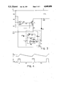
- FIG. 4 are waveforms showing the course of the voltage at the input and output of the relaxation voltage generator shown in FIG. 3;
- FIG. 5 shows an alternative embodiment of the circuit of FIG. 3 employing a bipolar transistor in lieu of a field-effect transistor.
- a "central office" 1 of the public communication network is indicated by a dash-dot line.
- This central office includes a source of dc voltage UB which supplies a constant dc voltage of, for instance, 95 V, which varies by at most 2 volts.
- eight PCM2 devices 3 are connected in parallel with each other to the source of dc voltage UB. From each PCM2 device 3 a subscriber's line ASL goes to in each case two subscribers who can also telephone simultaneously by digital transmission.
- each of the PCM2 devices 3 there is contained, for instance, a circuit in accordance with in FIG. 2. It has an active current-limiting component 4 which lies in series with an ohmic resistor R1.
- the word "component” has been selected for the sake of brevity. It includes a complete electronic circuit by which a controlled limiting of current can be carried out.
- the component 4 is connected to the source of dc voltage UB via a voltage divider, consisting of the resistors R2, R3 and R4, which is in parallel to said source of dc voltage UB.
- the feed voltage UB1 is connected to the subscriber's line ASL, it corresponding, except for a slight drop on the resistor R1 and on the component R4, to the voltage of the source of dc voltage UB.
- a relaxation generator K having an input E1.
- An input E2 of the relaxation generator K is connected, via the voltage divider formed by the resistors R2, R3 and R4, to the source of dc voltage UB, the input E2 being connected between the resistors R2 and R3.
- the output A of the relaxation voltage generator K is connected to the current-limiting component 4.
- the circuit of FIG. 2 operates as follows:
- the component 4 passes current.
- the feed voltage UB1 corresponds, except for a slight voltage drop over the resistor R1 and the component R4, to the operating voltage which is supplied by the source of dc voltage UB of the central office 1.
- the circuit limits the current flowing over the component 4. Due to the heating of the component 4 which takes place in the connection, this must not continue for too long. This is taken care of by the relaxation generator K, which does not operate in the event of normal operation. No influencing of the current-limiting component 4 then takes place.
- the current-limiting component 4 can be a bipolar transistor. However, a field-effect transistor can also be used. In the preferred embodiment, the component 4 is a MOSFET, as shown in FIG. 3.
- the current-limiting component 4 in this embodiment is a MOSFET T1 the current path of which is in series with the ohmic resistor R1.
- the resistor R1 is connected on the other side to the same pole of the source of dc voltage UB as the resistor R4.
- the output of the operational amplifier OP1 is connected via a resistor R5 to the gate electrode G of the MOSFET T1.
- the second input 02 of the operational amplifier OP1 is connected to the current path between the MOSFET T1 and the resistor R1. In the normal case, the voltage at the input 01 of the operational amplifier OP1 is greater than the voltage at the input 02.
- the MOSFET T1 then passes fully the current.
- the relaxation generator K provides at its output A, for instance, pulse-shaped voltage UA in accordance with FIG. 4b, by which the MOSFET T1 is held in its current-limiting condition only for a relatively short period of time. In a period of time which is not longer than this short time, the MOSFET T1 is blocked. No current then flows any longer over the MOSFET T1 (except for a negligible leakage current), so that the MOSFET T1, as a whole, is not substantially heated.
- an operational amplifier OP2 whose output forms the output A of the relaxation generator K.
- the one input 03 of the operational amplifier OP2 is connected, via an ohmic resistor R6, between the resistors R2 and R3 to the voltage divider R2/R3/R4, while the other input 04 is connected via a diode D1 to the drain electrode D of the MOSFET T1.
- a capacitor C which is connected on the other side to a pole of the source of dc voltage UB.
- the input 04 and the output of the operational amplifier OP2 are connected to each other, on the one hand, via the series connection of a diode D2 and an ohmic resistor R7 and, on the other hand, in a parallel branch via an ohmic resistor R8.
- the value of the resistor R7 is in the present case small as compared with that of the resistor R8.
- the relaxation generator K is connected via the diode D1 to the drain electrode D of the MOSFET T1.
- the diode D1 conducts during the normal operation of the circuit so that a high voltage is present at the output A of the relaxation generator K.
- the diode D3 which is connected between the output A of the relaxation voltage generator K and the control electrode of the MOSFET T1 is then blocked.
- the MOSFET T1 is operative for its task of limiting the current. It can therefore be low ohmic with full passage of current or high ohmic in its limiting function.
- the potential at the input 03 depends on a voltage divider comprising the resistors R6 and R9.
- the input 03 is connected to the voltage divider between the resistors R6 and R9.
- the voltage divider itself is connected to the output of the operational amplifier OP2 via resistor R9 and to the input E2 of the relaxation generator K via resistor R6.
- the potential of the input E2 of the relaxation generator K corresponds to the voltage tapped off between the resistors R2 and R3. During each phase in the operation of the circuit this voltage remains constant, within a permissible range of the variation of the source of dc voltage UB. A positive potential is then present at the output of the operational amplifier OP2.
- the diode D3 is blocked and does not affect the MOSFET T1.
- FIG. 5 shows the same circuit as FIG. 3 except that the transistor T1 is shown as a bipolar transistor in FIG. 5 instead of the field effect transistor of FIG. 3.
- the operational amplifier OP2 switches. A lower potential is present at its output, the diode D3 becomes conductive and the MOSFET T1 is blocked.
- the capacitor C is now discharged over the resistor R8 with the course of voltage shown in FIG. 4a.
- the discharge time t2 (FIG. 4b)
- low potential is present at the output of the operational amplifier OP2 and the MOSFET T1 remains blocked for the entire time.
- the operational OP2 moves back into its initial position with the high potential at the output, so that the MOSFET T1 is again brought into its current-limiting state.
- the times t1 and t2 can be in a ratio of, for instance, 1:5 to 1:10. This ratio can easily be set by suitable selection of the resistors R7 and R8.
- the resistor R7 should be small value as compared with the resistor R8 so that the capacitor C can be rapidly charged. The shorter time required for this determines the current-limiting time of the MOSFET T1 with less time for heating. The discharge of the capacitor C takes place, due to the diode D2, only over the resistor R8. If it is desired, for any reason, for the time t1 to be longer than the time t2, it is merely necessary to reverse the polarity of the diode D2.
- two separate voltage dividers can also be connected, in parallel to each other, to the source of dc voltage UB. One of them is then provided for the operational amplifier OP1 while the operational amplifier OP2 is connected to the other.
Landscapes
- Engineering & Computer Science (AREA)
- Power Engineering (AREA)
- Signal Processing (AREA)
- Emergency Protection Circuit Devices (AREA)
- Control Of Electric Motors In General (AREA)
- Electronic Switches (AREA)
- Devices For Supply Of Signal Current (AREA)
- Amplifiers (AREA)
- Control Of Electrical Variables (AREA)
Applications Claiming Priority (2)
| Application Number | Priority Date | Filing Date | Title |
|---|---|---|---|
| DE19863642624 DE3642624A1 (de) | 1986-12-13 | 1986-12-13 | Schaltungsanordnung zum Schutz elektronischer Geraete gegen UEberlastung |
| DE3642624 | 1986-12-13 |
Publications (1)
| Publication Number | Publication Date |
|---|---|
| US4849850A true US4849850A (en) | 1989-07-18 |
Family
ID=6316119
Family Applications (1)
| Application Number | Title | Priority Date | Filing Date |
|---|---|---|---|
| US07/132,245 Expired - Fee Related US4849850A (en) | 1986-12-13 | 1987-12-14 | Circuit for protecting electronic devices against overload |
Country Status (8)
| Country | Link |
|---|---|
| US (1) | US4849850A (fr) |
| EP (1) | EP0275352B1 (fr) |
| CN (1) | CN1007770B (fr) |
| AT (1) | ATE77010T1 (fr) |
| DE (2) | DE3642624A1 (fr) |
| DK (1) | DK652987A (fr) |
| ES (1) | ES2033743T3 (fr) |
| GR (1) | GR3004857T3 (fr) |
Cited By (11)
| Publication number | Priority date | Publication date | Assignee | Title |
|---|---|---|---|---|
| US4977477A (en) * | 1989-08-03 | 1990-12-11 | Motorola, Inc. | Short-circuit protected switched output circuit |
| US5192901A (en) * | 1990-03-16 | 1993-03-09 | Cherry Semiconductor Corporation | Short circuit protection |
| US5204636A (en) * | 1992-05-05 | 1993-04-20 | Xerox Corporation | Dynamic limiting circuit for an amplifier |
| US5299087A (en) * | 1990-08-29 | 1994-03-29 | International Business Machines Corporation | Overload protection circuit |
| EP0658031A1 (fr) * | 1993-12-13 | 1995-06-14 | Siemens Aktiengesellschaft | Dispositif de téléalimentation pour systèmes de communication |
| DE19532156C1 (de) * | 1995-08-31 | 1996-10-24 | Siemens Ag | Speiseschaltung für Kommunikationseinrichtungen |
| EP0913753A1 (fr) * | 1997-10-29 | 1999-05-06 | STMicroelectronics S.r.l. | Circuit de régulation électronique pour commander un dispositif de puissance et méthode de protection correspondante pour un tel dispositif |
| US6744229B2 (en) * | 2002-03-28 | 2004-06-01 | Sunonwealth Electric Machine Industry Co., Ltd | Safety-guard detective circuit of a fan motor |
| US20090103223A1 (en) * | 2006-05-12 | 2009-04-23 | Beckhoff Automation Gmbh | Power circuit with short-circuit protection circuit |
| US7843248B1 (en) * | 2007-11-01 | 2010-11-30 | Intersil Americas Inc. | Analog switch with overcurrent detection |
| US11271390B2 (en) * | 2016-07-29 | 2022-03-08 | Endress+Hauser Flowtec Ag | Intrinsically safe circuit arrangement |
Families Citing this family (3)
| Publication number | Priority date | Publication date | Assignee | Title |
|---|---|---|---|---|
| DE4138989A1 (de) * | 1991-11-27 | 1993-06-03 | Ant Nachrichtentech | Verfahren zur begrenzung des stromes ueber ein stellglied sowie anordnung |
| DE4431077C1 (de) * | 1994-09-01 | 1995-08-31 | Ant Nachrichtentech | Überstrombegrenzungseinrichtung |
| DE29909206U1 (de) | 1999-05-28 | 2000-10-05 | Ellenberger & Poensgen | Schutzeinrichtung |
Citations (3)
| Publication number | Priority date | Publication date | Assignee | Title |
|---|---|---|---|---|
| US4430682A (en) * | 1980-11-03 | 1984-02-07 | Mannesmann Ag | Protection circuit for d.c. motors |
| US4709160A (en) * | 1986-08-25 | 1987-11-24 | Rockwell International Corporation | Solid state dc power switch |
| US4718084A (en) * | 1984-12-19 | 1988-01-05 | Siemens Aktiengesellschaft | Overload protection circuit for a telephone subscriber line feed circuit |
Family Cites Families (5)
| Publication number | Priority date | Publication date | Assignee | Title |
|---|---|---|---|---|
| DE2360678B2 (de) * | 1973-12-05 | 1978-04-27 | Siemens Ag, 1000 Berlin Und 8000 Muenchen | Schaltungsanordnung zur Kurzschluß- und Überlastsicherung eines elektronischen Leistungsschaltkreises mit einer Endstufe |
| US4019096A (en) * | 1976-06-07 | 1977-04-19 | Rockwell International Corporation | Current limiting apparatus |
| DE2648102A1 (de) * | 1976-10-23 | 1978-04-27 | Bbc Brown Boveri & Cie | Anordnung zur optimalen leistungsabgabe im ueberlastbereich bei kurzschluss- und ueberlastgeschuetzten leistungsschaltstufen |
| DE3121754C1 (de) * | 1981-06-01 | 1982-12-09 | Siemens AG, 1000 Berlin und 8000 München | Leistungsschalter mit einem Feldeffekttransistor |
| US4394703A (en) * | 1981-12-24 | 1983-07-19 | Gte Automatic Electric Labs Inc. | Load protecting arrangement |
-
1986
- 1986-12-13 DE DE19863642624 patent/DE3642624A1/de not_active Withdrawn
-
1987
- 1987-07-01 AT AT87109446T patent/ATE77010T1/de not_active IP Right Cessation
- 1987-07-01 EP EP87109446A patent/EP0275352B1/fr not_active Expired - Lifetime
- 1987-07-01 ES ES198787109446T patent/ES2033743T3/es not_active Expired - Lifetime
- 1987-07-01 DE DE87109446T patent/DE3779606D1/de not_active Expired - Lifetime
- 1987-12-11 DK DK652987A patent/DK652987A/da not_active Application Discontinuation
- 1987-12-12 CN CN87107404A patent/CN1007770B/zh not_active Expired
- 1987-12-14 US US07/132,245 patent/US4849850A/en not_active Expired - Fee Related
-
1992
- 1992-06-10 GR GR920401210T patent/GR3004857T3/el unknown
Patent Citations (3)
| Publication number | Priority date | Publication date | Assignee | Title |
|---|---|---|---|---|
| US4430682A (en) * | 1980-11-03 | 1984-02-07 | Mannesmann Ag | Protection circuit for d.c. motors |
| US4718084A (en) * | 1984-12-19 | 1988-01-05 | Siemens Aktiengesellschaft | Overload protection circuit for a telephone subscriber line feed circuit |
| US4709160A (en) * | 1986-08-25 | 1987-11-24 | Rockwell International Corporation | Solid state dc power switch |
Cited By (13)
| Publication number | Priority date | Publication date | Assignee | Title |
|---|---|---|---|---|
| US4977477A (en) * | 1989-08-03 | 1990-12-11 | Motorola, Inc. | Short-circuit protected switched output circuit |
| US5192901A (en) * | 1990-03-16 | 1993-03-09 | Cherry Semiconductor Corporation | Short circuit protection |
| US5299087A (en) * | 1990-08-29 | 1994-03-29 | International Business Machines Corporation | Overload protection circuit |
| US5204636A (en) * | 1992-05-05 | 1993-04-20 | Xerox Corporation | Dynamic limiting circuit for an amplifier |
| EP0658031A1 (fr) * | 1993-12-13 | 1995-06-14 | Siemens Aktiengesellschaft | Dispositif de téléalimentation pour systèmes de communication |
| DE19532156C1 (de) * | 1995-08-31 | 1996-10-24 | Siemens Ag | Speiseschaltung für Kommunikationseinrichtungen |
| EP0913753A1 (fr) * | 1997-10-29 | 1999-05-06 | STMicroelectronics S.r.l. | Circuit de régulation électronique pour commander un dispositif de puissance et méthode de protection correspondante pour un tel dispositif |
| US6118642A (en) * | 1997-10-29 | 2000-09-12 | Stmicroelectronics, S.R.L. | Electronic regulation circuit for driving a power device and corresponding protection method of such device |
| US6744229B2 (en) * | 2002-03-28 | 2004-06-01 | Sunonwealth Electric Machine Industry Co., Ltd | Safety-guard detective circuit of a fan motor |
| US20090103223A1 (en) * | 2006-05-12 | 2009-04-23 | Beckhoff Automation Gmbh | Power circuit with short-circuit protection circuit |
| US9184740B2 (en) * | 2006-05-12 | 2015-11-10 | Beckhoff Automation Gmbh | Power circuit with short-circuit protection circuit |
| US7843248B1 (en) * | 2007-11-01 | 2010-11-30 | Intersil Americas Inc. | Analog switch with overcurrent detection |
| US11271390B2 (en) * | 2016-07-29 | 2022-03-08 | Endress+Hauser Flowtec Ag | Intrinsically safe circuit arrangement |
Also Published As
| Publication number | Publication date |
|---|---|
| EP0275352A1 (fr) | 1988-07-27 |
| DE3642624A1 (de) | 1988-06-23 |
| ES2033743T3 (es) | 1993-04-01 |
| CN1007770B (zh) | 1990-04-25 |
| DK652987A (da) | 1988-06-14 |
| EP0275352B1 (fr) | 1992-06-03 |
| DE3779606D1 (en) | 1992-07-09 |
| ATE77010T1 (de) | 1992-06-15 |
| GR3004857T3 (fr) | 1993-04-28 |
| DK652987D0 (da) | 1987-12-11 |
| CN87107404A (zh) | 1988-06-29 |
Similar Documents
| Publication | Publication Date | Title |
|---|---|---|
| US4849850A (en) | Circuit for protecting electronic devices against overload | |
| US5659608A (en) | Line feed circuit with logic level controlled ringing | |
| US5721774A (en) | Longitudinally balanced, dual voltage line-feed circuit | |
| US3859586A (en) | Overcurrent protection circuit utilizing peak detection circuit with variable dynamic response | |
| US4349703A (en) | Programmable ring signal generator | |
| US4431868A (en) | Solid state telephone line interface circuit with ringing capability | |
| KR970003191B1 (ko) | 비상 상태가 극성 반전으로 표시되는 비상 d.c. 전원 공급기 | |
| US4315107A (en) | Telephone range extender with gain | |
| US5706157A (en) | Power distribution system with over-current protection | |
| US4306119A (en) | Telephone outpulsing circuit | |
| US5798578A (en) | Synchronization device for a redundant power supply system | |
| US20010012192A1 (en) | Active current limiter | |
| US4761812A (en) | Constant power telephone line circuit | |
| EP0102111B1 (fr) | Circuit pour téléphone | |
| US4355240A (en) | Auxiliary backup regulator control for paralleled converter circuits controlled by a master regulator | |
| US4143239A (en) | Signal distortion correction circuit in teleprinter equipment | |
| GB2052213A (en) | Three-terminal power supply circuit for telephone set | |
| EP0671088A1 (fr) | Circuit pour la commande d'un ensemble de recepteurs, notamment de regulateurs de puissance de lampes. | |
| EP0102660B1 (fr) | Circuit pour téléphone | |
| US5113426A (en) | Ground fault detector | |
| EP0105336B1 (fr) | Circuit generateur d'impulsions pour composer un numero telephonique | |
| US5726853A (en) | High voltage protection circuit for telephone test set | |
| US4388497A (en) | Telephone power supply arrangement | |
| US5221886A (en) | Device for regulating the battery charging voltage delivered by an alternator | |
| US6239648B1 (en) | System and method for dissipating heat in an electric device |
Legal Events
| Date | Code | Title | Description |
|---|---|---|---|
| AS | Assignment |
Owner name: KABELMETAL ELECTRO GESELLSCHAFT MIT BESCHRANKTER H Free format text: ASSIGNMENT OF ASSIGNORS INTEREST.;ASSIGNOR:BRAHMS, MARTIN;REEL/FRAME:004848/0077 Effective date: 19880102 Owner name: KABELMETAL ELECTRO GESELLSCHAFT MIT BESCHRANKTER H Free format text: ASSIGNMENT OF ASSIGNORS INTEREST;ASSIGNOR:BRAHMS, MARTIN;REEL/FRAME:004848/0077 Effective date: 19880102 |
|
| FPAY | Fee payment |
Year of fee payment: 4 |
|
| REMI | Maintenance fee reminder mailed | ||
| REMI | Maintenance fee reminder mailed | ||
| LAPS | Lapse for failure to pay maintenance fees | ||
| FP | Lapsed due to failure to pay maintenance fee |
Effective date: 19970723 |
|
| STCH | Information on status: patent discontinuation |
Free format text: PATENT EXPIRED DUE TO NONPAYMENT OF MAINTENANCE FEES UNDER 37 CFR 1.362 |