US4849922A - Circuit for computing the quantized coefficient discrete cosine transform of digital signal samples - Google Patents
Circuit for computing the quantized coefficient discrete cosine transform of digital signal samples Download PDFInfo
- Publication number
- US4849922A US4849922A US07/131,833 US13183387A US4849922A US 4849922 A US4849922 A US 4849922A US 13183387 A US13183387 A US 13183387A US 4849922 A US4849922 A US 4849922A
- Authority
- US
- United States
- Prior art keywords
- adder
- subtracter
- input
- outputs
- units
- Prior art date
- Legal status (The legal status is an assumption and is not a legal conclusion. Google has not performed a legal analysis and makes no representation as to the accuracy of the status listed.)
- Expired - Fee Related
Links
Images
Classifications
-
- G—PHYSICS
- G06—COMPUTING OR CALCULATING; COUNTING
- G06F—ELECTRIC DIGITAL DATA PROCESSING
- G06F17/00—Digital computing or data processing equipment or methods, specially adapted for specific functions
- G06F17/10—Complex mathematical operations
- G06F17/14—Fourier, Walsh or analogous domain transformations, e.g. Laplace, Hilbert, Karhunen-Loeve, transforms
- G06F17/147—Discrete orthonormal transforms, e.g. discrete cosine transform, discrete sine transform, and variations therefrom, e.g. modified discrete cosine transform, integer transforms approximating the discrete cosine transform
-
- G—PHYSICS
- G06—COMPUTING OR CALCULATING; COUNTING
- G06F—ELECTRIC DIGITAL DATA PROCESSING
- G06F7/00—Methods or arrangements for processing data by operating upon the order or content of the data handled
- G06F7/38—Methods or arrangements for performing computations using exclusively denominational number representation, e.g. using binary, ternary, decimal representation
- G06F7/48—Methods or arrangements for performing computations using exclusively denominational number representation, e.g. using binary, ternary, decimal representation using non-contact-making devices, e.g. tube, solid state device; using unspecified devices
- G06F7/52—Multiplying; Dividing
- G06F7/523—Multiplying only
- G06F7/533—Reduction of the number of iteration steps or stages, e.g. using the Booth algorithm, log-sum, odd-even
- G06F7/5334—Reduction of the number of iteration steps or stages, e.g. using the Booth algorithm, log-sum, odd-even by using multiple bit scanning, i.e. by decoding groups of successive multiplier bits in order to select an appropriate precalculated multiple of the multiplicand as a partial product
Definitions
- the present invention relates to digital signal coding.
- it relates to a circuit for computing the quantized coefficient discrete cosine transform of digital signal samples.
- Transform digital coding applied to blocks of one-, two-, and three-dimensional digital signal samples is widely used in all applications, e.g. video signal processing which requires spectral analysis, data compression, and reduction of original signal bandwidth.
- transform coding The various types of transform coding are well known. They include the Hadamard or HCT (High Correlation Transform) types, which are based on extremely simple coefficients, and Fourier transform, which requires complicated floating point calculations. Yet other types include the Slant transform, which concerns optimal frequency spectrum energy distribution.
- HCT High Correlation Transform
- the discrete cosine transform referred to hereunder as the DCT transform
- the DCT transform provides the best compromise between effective representation in the transform signal frequency spectrum and simplicity of construction in many applications, including video signal processing.
- the major advantage consists in the recurrence of its N real coefficients.
- DCT transform computational algorithms are used; some are based on its direct derivation from the Fourier transform, while others exploit coefficient recurrence. These algorithms all serve to reduce the number of multiplications by comparison with the total number of operations to be carried out (addition, accumulation, addressing, normalizing, rounding off and cut-off operations); this makes them particularly suitable for software applications whose major objective is to reduce the number of microinstruction cycles.
- N.N bit multiplication operation involves converting this operation into a sequence of N elementary N-bit adding and shifting operations. This solution has been used in parallel type multipliers with various circuit optimizations.
- Another object is to provide a DCT transform computation circuit with which it is possible to reduce space requirements, computing time and power dissipation.
- each multiplication according to the invention is performed by means of an addition and shifting operation which involves the sample to be transformed on input and/or the results of previous multiplications.
- the number of operations to be performed is thus drastically reduced, reordering the various intermediate products to be accumulated does not become more complicated, and creating accumulation memory addressing units also remains simple. This can be achieved using VLSI circuits.
- the same circuit can be used to compute the DCT transform at any number of dimensions.
- a circuit for computing a discrete cosine transform of f(j) sample vectors of dimension N(0 ⁇ j ⁇ N-1), the transform having a square matrix base of dimensions N.N with coefficients which repeat in absolute value at each column but whose order (and in some cases sign) differ, the circuit obtaining transformed F(k) sample vectors, also of dimension N(0 ⁇ k ⁇ N-1).
- the circuit consists of two circuit branches working in parallel, the first for operations relating to coefficients in even matrix lines, the second for coefficient in odd lines.
- the two branches consist essentially of:
- a first adder and a first subtracter belonging to the first and second branch respectively, which at inputs receive pairs of samples of an F(j) vector having index (j) and (N-j-1), with j increasing sequentially from 0 to NR-1;
- first and second calculating units belonging to the first and second branch respectively, which, for each addition or subtraction result received respectively from the first adder or first subtracter, calculate NR partial products referring to the matrix column coefficients in even and odd lines respectively, with sequential order, among the coefficients of a column, fixed for all columns, so as to produce each partial product through an addition and shifting operation which involves the previous partial products and/or input datum;
- a first and second adder/subtracter belonging respectively to the first and second branch which add or subtract a partial product received from a second input to or from a datum received from a first input of first and second calculating units respectively, and finding the sum in the case of a partial product referring to a positive coefficient, or the difference in the case of a negative coefficient;
- first and second memories belonging to the first and second branch respectively, accumulating NR partial results each, for accumulating calculations performed by the first and second adder/subtracters, the first memories accumulating partial results R*(2k) relating to even matrix column lines, the second memories accumulating partial result R*(2k+1) relating to odd lines, the partial results being componentsof a transformed sample vector F(k) at the NR-1 index columns;
- first addressing units which generate: first control signals for the first and second calculating units, the first control signals determining the sequential order, among coefficients of a column, fixed for all columns; addresses to be read in the first and second memories for accumulation of the partial results, supplied as data to the first input of first and second adder/subtracter respectively, and for re-writing them updated in the same position, the addresses having a sequence which varies with the matrix column, such as to identify the partial result R*(2k) and R*(2k+1) whose index corresponds to the matrix line containing the coefficient for which the first and second calculating units perform the partial products; operation selection signals for the first and second adder/subtracter.
- the first circuit units consist of:
- a first and a second multiplexer which at a a first input receive output of the first adder and at a second input receive output of a first register
- first and second shifting units which receive outputs of the first and second multiplexer respectively
- the second circuit units include:
- a third and fourth multiplexers which at a first input receive output of the first subtracter, the third multiplexer receiving at a second input the output of a second register, the fourth multiplexer also receiving the outputs of a third and fourth register at a third and fourth input;
- third and fourth shifting units which receive outputs of the third and fourth multiplexers respectively
- a fourth adder/subtracter which receives outputs of the third and fourth shifting units, for subtraction subtracting the output of the third shifting units from that of the fourth shifting units and whose output supplies the second, third and fourth registers and is the output of the second circuit units, the first, second, third and fourth registers being used for temporary storage of the previous partial products.
- the first control signals generated by the first addressing units cause the following succession of operations to be performed by the first and second calculating units: for the first partial product, the first, second, third and fourth multiplexers are switched on the first input, the first, second, third and fourth shifting units shift respectively by four, one zero and three positions to the left, in the direction of multiplications by powers of two, the third and fourth adder/subtracter find the sum, the first and second registers memorize the input datum; for the second partial product the first, second, third and fourth multiplexers are switched respectively on the second, first, second, first input, the first, second, third and fourth shifting units shift respectively by one, zero, one and three positions to the left, the third and fourth adder/subtracters find the sum and the difference respectively, the third register memorizes the input data; for the third partial product the first, second, third and fourth multiplexers are switched on the second, first, second and third input, the first, second, third and fourth shifting units shift by zero, five, zero and one positions to the left, the third
- the first and second circuit units can include six and eight adders or subtracters respectively which produce an equal number of partial products through suitable justification of their two inputs, six and eighth registers which memorizes the results thereof, and further register on input of the first circuit units and multiplexers which receive the outputs of the registers, the first control signals generated by the addressing units determining only the connection sequence of multiplexer inputs with outputs.
- the first circuit units can have the following interconnections between the adders or subtracters, intercalated with the registers; to a second adder is applied the output of the first adder shifted to the left by one and four positions; to a third adder are brought the outputs of the first adder, shifted by five positions to the left, and of the second adder; to a second subtracter are brought the outputs of the second adder, shifted by one position to the left, and of the first adder; to a third subtracter are brought the outputs of the first adder, shifted by four positions to the left, and of the third adder, shifted by one position to the left; to a fourth adder are connected to the outputs of the first adder, shifted by six positions to the left, and of the third adder, shifted by one position to the right; and to a fifth adder is applied the output of the third adder shifted by one position to the right at one input; the further register receives the output of the first adder shifted by six positions to the left.
- the second circuit units have the following interconnection between the adders and subtracters, intercalated with the registers: to a sixth and seventh adder is applied the output of the first subtracter respectively shifted by six and four positions to the left and by three and zero positions to the left; to an eighth adder are brought the outputs of the first subtracter, shifted by three positions to the left, and of the seventh adder, shifted by one position to the left; to a fourth subtracter are brought the outputs of the first subtracter, shifted by one position to the left, and of the seventh adder, shifted by three positions to the left; to a fifth subtracter are applied the outputs of the seventh adder and the eight adder, shifted by one position to the left; to a ninth adder are brought the outputs of the first subtracter, shifted by six positions to the left, and of the eighth adder: to a tenth adder are applied the outputs of the sixth adder, shifted by four positions to the right and of the eighth adder, shifted by one position to the left;
- the first circuit units can include:
- a fifth and a sixth multiplexer who receive at a first input output of the first adder, at a second input output of a fifth register; the sixth multiplexer receiving at a third input output of a sixth register shifted by one position to the left, and with the outputs applied to its first ans second inputs shifted by three positions to the left;
- fifth scaling units which receive output of the fifth multiplexer
- a sixth subtracter which subtracts the output of the fifth shifting units from that of the sixth multiplexer, and whose output supplies the fifth and sixth registers and is the output of the first circuit units.
- the second circuit units include:
- a seventh and an eighth multiplexer which receive at a first input output of the first subtracter, and at a second input outputs of a seventh and an eight register respectively;
- sixth and seventh shifting units which receive respectively the outputs of the seventh and eight multiplexers
- a sixth adder/subtracter which receives the outputs of the sixth and seventh shifting units, for subtraction subtracting the output of the sixth shifting units from that of the seventh, and whose output supplies the seventh and eighth registers and is the output of the second circuit units; the fifth, sixth, seventh, eighth registers being used for temporary storage of the previous partial products.
- the first control signals generated by the addressing units cause the following succession of operations on the part of the first and second calculating units: for the first partial product, the fifth, sixth, seventh and eighth multiplexers are switched on the first input, the fifth, sixth, and seventh shifting units shift by zero, zero and three positions to the left, the sixth adder/subtracter performs subtraction, the fifth and seventh registers memorize the input datum; for the second partial product, the fifth, sixth, seventh multiplexers are switched on the second input, the eighth multiplexer on the first input, the fifth, sixth and seventh shifting units shift by zero, zero and five positions, the sixth adder/subtracter performs subtraction, the sixth and eighth registers memorize the input datum; for the third partial product, the fifth, sixth, seventh and eight multiplexers are switched respectively on the second, third, second and fifth inputs, the fifth, sixth and seventh shifting units shift by zero, zero and six positions to the left, the sixth adder/subtracter finds the sum; for the fourth partial product, the fifth, sixth, seventh and
- the first and second circuit units can include respectively four and five adders or subtracters which produce an equal number of partial products through suitable justification of their two inputs, four and five registers which memorize the results thereof, and an output multiplexer which receives the outputs of the registers, the first control signals generated by the addressing units determining only the connection sequence of multiplexer inputs with outputs.
- the first circuit units have the following interconnection between the adders or subtracters, intercalated with the registers: to a seventh subtracter is applied the output of the first adder shifted by three positions to the left at one input; to an eight subtracter is applied the output of the seventh subtracter shifted at an input by three positions; to a ninth subtracter are applied the outputs of the seventh subtracter, and the eighth subtracter scaled by one position to the left; and to a tenth subtracter are brought the outputs of the first adder, shifted by six positions to the left, and of the ninth subtracter shifted by one position to the left.
- the second circuit units can then have the following interconnection between the adders or subtracters, intercalated with the registers: to an eleventh and twelfth subtracter is applied the output of the first subtracter respectively shifted by three, zero, seven and one position to the left; to a thirteenth subtracter are applied the outputs of the first adder, shifted by five positions to the left, and the eleventh subtracter; to a twelfth adder are applied the outputs of the first subtracter, shifted by six positions to the left, and of the eleventh subtracter; to a thirteenth subtracter are applied the outputs of the eleventh subtracter shifted by three positions to the left, and of the thirteenth subtracter, shifted by one position to the left; the output multiplexer connecting inputs to outputs in the following order: for the first partial product, the outputs of the eighth and thirteenth subtracters; for the second partial product, the outputs of the ninth subtracter and the twelfth adder; for the third partial product, the outputs of the ninth subtracter and the
- the first addressing units supply to the outside a data-ready (DR) signal at the beginning of the operations relating to the NR-1 index column; on the basis of the signal, the partial results R*(k) at the outputs of the first and second adder/subtracters are available at outputs as components of a transformed F(k) sample vector.
- DR data-ready
- These first addressing units supply, at the end of calculations relating to the index NR-1 column, addresses to the first and second accumulation memories for sequential reading and forwarding to the outputs of R*(k) partial results, there memorized, as components of a transformed F(k) sample vector.
- the data at the outputs of the first adder, first subtracter, first and second calculating units and first and second accumulation memories are synchronized by registers.
- the shifting units can consist of barrel shifters.
- the two-dimensional discrete cosine transform circuits can include a first of the circuits followed by a matrix-structured intermediate memory and by a second of such circuits, and second addressing units for the intermediate memory which determine writing of N vectors of transformed F(k) samples, calculated by the first circuit, and reading in a direction orthogonal to that of writing, of N vectors of f(j) samples to be transformed, each consisting for the K-nth component of the F(k) vectors present in the intermediate memory, for forwarding to the second circuit (DCT2).
- DCT2 second circuit
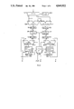
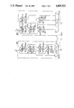
- FIG. 1 is a block diagram of the one-dimensional DCT transform computational circuit described herein;
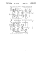
- FIGS. 2, 3, 4 and 5 show embodiments of the ERM and ORM blocks of FIG. 1, which perform multiplication operations
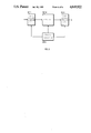
- FIG. 6 shows an embodiment of the two-dimensional DCT transform computational circuit using two circuits as shown in FIG. 1.
- each coefficient of a column can be obtained from the preceding coefficients by means of a single addition and shifting operation, keeping the odd matrix lines separate from the even lines at all times; the first coefficient of both even and odd lines is broken down in a sum of two power-of-two values.
- Coefficient 70 is taken with a negative sign for reasons which will be clarified later.
- the transformation algorithms for the one-dimensional case consists in computing the matrix product of a sequence of N-component column vectors (representing the sequence of input signals to be transformed) and the transform coefficient matrix of dimensions N.N, obtaining another N-component column vector: with the known circuits discussed above, this is generally carried out by multiplying and accumulating each input vector component by all terms of the corresponding matrix line, moving sequentially by line inside the matrix.
- a memory with a capacity of N words is required for temporarily storage of intermediate accumulations, as all partial contributions of each f(k) component must be computed simultaneously for each f(j) input sample.
- the two-dimensional transform requires a further N.N word capacity memory between the two orthogonal transformation processes, as the second transform step must be applied to the N vectors transposed for the one-dimensional case.
- each word is (log N+Nb+Ns) bits, where log N may be 4 or 3, Nb is in our case equal to 8 and is the precision of the coefficients, and Ns is the precision of the input samples.
- this type of approach permits easy address generation and management, so that further complications do not arise in developing the internal addressing unit of the circuit.
- MEM1 is a memory in which are written the N vector components of the f(j) samples to be transformed; said components are addressed during reading by an addressing unit ADR1 so that output buses 1 and 2 simultaneously hold components of index f(j) and f(N-j-1) respectively, with j increasing sequentially from 0 to (N/2-1).
- SOM1 is a normal adder for MEM1 outputs 1 and 2, while SOT1 is a normal subtracter which subtracts MEM1 output 2 from output 1.
- Registers RG1 and RG2 are two normal registers for temporary storage of outputs of SOM1 and SOT1 respectively.
- ERM and ORM are two crcuits capable of pseudo-multiplying input sample vector components by transformation matrix coefficients in accordance with this invention; ERM is used for the even lines of the matrix and receives samples from RG1 output 3, while ORM is used for odd lines and receives samples from RG2 output 4.
- RG3 and RG4 are two normal registers for temporary storage of results of operations carried out by circuits ERM and ORM, respectively available on outputs 5 and 6 of said circuits. RG3 supplies data on output 8, and RG4 on output 9.
- SMST1 and SMST2 are normal adder/subtractors which add input 8 to input 10 and input 9 to input 11, or subtract input 8 from 10 and 9 from 11.
- Choice of operations is controlled by block ADR2: the sum is performed at the positive coefficients of the transform, while subtraction takes place at the negative coefficients.
- MEM2 and MEM3 are two memories for accumulating the partial results R(k) of the sum/subtractions performed by SMST1 and SMST2.
- MEM2 memorizes N/2 partial results R(2k) relating to contributions of even coefficient matrix lines, while MEM3 memorizes N/2 partial results R(2k+1) of the odd lines (0 ⁇ k ⁇ N/2-1).
- MEM2 and MEM3 are line-structured, with one line for each index k.
- RG5 and RG6 are two registers for temporarystorage of partial results R(2 K) and R(2k+1) read in memories MEM2 and MEM3 respectively.
- the various partial results are present at outputs 10 and 11 of RG5 and RG6.
- the N components of transform vector F(k) are present at outputs 12 and 13, and are divided into even index components F(2k) at output 12 and odd index components F(2k+1) at output 13.
- ADR2 is an address generating block which reads and writes memories MEM2 and MEM3, command signals for operations performed by blocks ERM and ORM, SMST1 and SMST2 operation selection signals and RG5 and RG6 output selection signals.
- ADR2 For each column of the transform coefficient matrix, ADR2 always supplies the same succession of command signals to blocks ERM and ORM to perform the sequence of operations shown as an example in Tables 3 and 4. Items which change as a function of matrix column include control of the operation performed by SMST1 and SMST2, and addressing of memories MEM2 and MEM3 by ADR2 in order to read partial results R(2k) and R(2k+1) of suitable index k.
- the MEM2 and MEM3 address reading sequence generated by ADR2 can be deduced easily from Tables 1, 2, 3 and 4 on the basis of the following considerations.
- the circuit shown in FIG. 1 is divided into two branches, relating respectively to the even and odd lines of the coefficient matrix; the branches work simultaneously.
- ADR2 thus simultaneously addresses pairs of partial results, one in MEM2 and one in MEM3.
- data at outputs 12 and 13 are already the final results of the transformation operation, but are in an unordered double sequence, i.e., with variable index k, which depends on the particular order of Table 3 or 4 sequence coefficients in the (N/2-1) column of Table 1 or 2.
- ADR2 then supplies the data-ready signal DR and addresses MEM2 and MEM3 in alternating sequence so as to provide the ordered sequence of N transform vector F(k) components at outputs 12 and 13.
- Controller ADR2 may consist of two counters, one for MEM2 and one for MEM3, which count in sequence from 0 to N/2-1 for each matrix column, followed by a combinatory logic which suitably changes bit justification at counter output in relation to the value of m(i.e., of the column).
- controller ADR2 may consist of a matrix-structured memory addressed sequentially in increasing order, first by column and then by line, and in which the pair of N values used to address MEM2 and MEM3 is written in every position.
- controller ADR2 Neither embodiment of controller ADR2 is a problem for technicians in the field, given the data description provided here.
- an external synchronizing unit of standard type which again will present no problems to the technician, is provided to supply a clock signal to the various sequential circuits and to the ADR2 block.
- this unit provides controller ADR2 with a start signal for computing an input sample vector f(j).
- blocks MEM1 and ADR1 are not an essential part of the DCT transform computational circuit, but represent a possible example of how the double sequence of f(j) vectors on inputs 1 and 2 can be achieved.
- circuit shown in FIG. 1 is set up using an integrated structure, it is advisable to confine these blocks outside of the integrated circuit. This is partly because they might be part of existing circuits and techniques used will thus depend on the specific case in hand. Care should be taken, however, to obtain the particular sequence of vector f(j) components described above at inputs 1 and 2.
- ERM consists of circuit blocks MX1, MX2, SH1, SH2, SMST3 and RG7, while ORM consists of circuit blocks MX3, MX4, SH3, SH4, SMST4, RG8, RG9 and RG10.
- MX1 and MX2 are two normal multiplexers, each of which receives output 3 of register RG1 (FIG. 1) and output 15 of register RG7.
- Shifter SH1 and SH2 are two circuits which shift a given variable number of input positions of the data applied to their input. Shifter SH1 receives the multiplexer MX1 output, while shifter SH2 receives the multiplexer MX2 output.
- SH1 and SH2 are barrel shifter circuits, consisting of a battery of multiplexers which shift a variable number of input positions in a brief, fixed period (which is the average data propagation time through their structure). The number of shift positions is determined by the bit combination applied to their control input. These circuits are used instead of normal shift registers because of their greater shifting speed.
- Outputs of shifters SH1 and SH2 are brought to a normal adder/subtracter SMST3, which adds the inputs or subtracts the shifter SH2 output from the shifter S1 output.
- the output of adder/subtracter SMST3 is output 5 of the ERM block, as well as the input of normal register RG7 which memorizes input data upon receiving a loading signal from connection 7, and whose data output 15 is connected to the inputs of multilexers MX1 and MX2.
- ORM block structure is similar to that of ERM, and consists of two multiplexers MX3 and MX4 followed by two barrel-shifters SH3 and SH4 which supplyan adder-subtracter SMST4; the latter adds inputs or subtracts the shifter SH3 output from the shifter SH4 output.
- the output of adder/subtracter SMST4 is ORM output 6, as well as the input of normal registers RG8, RG9 and RG10 which memorize input data upon receiving a loading signal from connection 1.
- the multiplexer MX3 receives the register RG2 output 4 (FIG. 1) and the register RG8 output 16, while the multiplexer MX4 receives the register RG9 outputs 4 and 17 and the register RG10 output 18.
- the controller ADR2 (FIG. 1) supplies on connection 7 the input selection signals of multiplexers MX1, MX2, MX3 and MX4, the bit connections determining the extent of shifting carried out by shifters SH1, SH2, SH3 and SH4, the loading signals for registers RG4, RG8, RG9 and RG10, and the addition/subtraction selection signals for adder/subtracters SMST3 and SMST4.
- Composition of the part of controller ADR2 wich generates signals on connection 7 can be readily deduced from the following description of ERM and ORM block operation.
- the ERM block multiplies coefficients in the right-hand column of Table 3, while ORM multiplies coefficients in the left-hand column, proceeding from top to bottom of the table.
- multiplexers MX1 and MX2 are both switched on input 3; shifter SH1 shifts by four positions towards the left (multiplication by 16), while shifter SH2 shifts by 1 position (multiplication by 2); adder/subtracter SMST3 then adds, while the result of the multiplication by 18 is on output 5, and is also temporarily stored in register RG7 and serves for subsequent input 3 datum multiplication by the second and third coefficients (35 and 50).
- multiplexer MX1 is switched on input 15 by register RG7, and multiplexer MX2 on input 3; shifter SH1 shifts by 1 position to the left, shifter SH2 does not shift positions, and adder/subtracter SMST3 finds the difference.
- multiplexer MX1 is switched on input 15 and multiplexer MX2 on input 3; shifter S1 does not shift positions, while shifter SH2 shifts 5 positions to the left; and adder/subtracter SMST3 adds the two inputs and the esult is stored in RG7 in place of the preceding, as well as being available at output 5.
- multiplexers MX1 and MX2 are switched on input 3; shifters SH1 and SH2 shift by five positions to the left, and SMST3 finds the sum.
- multiplexers MX1 and MX2 are switched on input 15; shifter SH1 shifts by one position to the right (division by 2), while shifter SH2 does not shift positions; adder/subtracter SMST3 finds the sum of the inputs.
- multilexer MX1 is switched on input 15 and MX2 on input 3; shifter SH1 shifts by one position, shifter SH2 by four positions to the left; and adder/subtracter SMST3 finds the difference.
- For the seventh coefficient (89) multiplexer MX1 is switched on input 15, multiplexer MX2 on input 3; shifter SH1 shifts 1 position to the right, and shifter SH2 shifts 6 positions to the left, and SMST3 finds the sum.
- multiplexers MX3 and MX4 are switched on input 4; shifter SH3 does not shift positions, shifter SH4 shifts by 3 positions to the left (multiplication by 8); adder/subtracter SMST4 finds the sum and the result, aside from being available at output 6, is also stored in register RG8 and serves for subsequent multiplication by the second, third and fourth coefficients (26, 43 and 70).
- multiplexer MX4 is switched on input 4, multiplexer MX3 on input 16; shifter SH3 shifts by 1 position to the left, shifter SH4 shifts by 3 positions to the left; and adder/subtracter SMST4 finds the sum and the results is also stored in register RG9.
- multiplexer MX3 is switched on input 16, multiplexer MX4 on input 17; shifter SH3 does not shift positions; shifter SH4 shifts by one position to the left; and adder/subtracter SMST4 finds the difference and the result is stored in register RG10.
- multiplexer MX4 is switched on input 4, multiplexer MX3 on input 16; shifter SH3 shifts by 3 positions to the left, shifter SH4 by 1 position to the left and adder/subtracter SMST4 finds the difference.
- the fourth coefficient is taken with a negative sign because otherwise it would be necessary to invert adder/subtracter SMST4 inputs, unnecessarily complicating the circuit.
- the correct sign of the product computed by multiplexer ORM is restored by a suitable add or subtract command from adder/subtracter SMST2 (FIG. 1) without further burdening the circuit.
- multiplexers MX3 and MX4 are switched on input 4; shifter SH3 and SH4 shift respectively by 4 ad 6 positions to the left; and adder/subtracter SMST4 finds the sum, and the result is stored in register RG8 in place of the preceding.
- multiplexer MX3 is switched on input 16, multiplexer MX4 on input 17; shifter SH3 shifts by 4 positions to the right (division by 16), shifter SH4 by 1 position to the left, and adder/subtracter SMST4 finds the sum.
- multiplexer MX3 is switched on input 4, multiplexer MX4 on input 18; shifter SH3 does not shift positions. Shifter SH4 shifts by one position to the left, and adder/subtracter SMST4 finds the sum.
- multiplexer MX3 is switched on input 4; multiplexer MX4 on input 17; shifter SH3 shifts by 6 positions to the left, shifter SH4 does not shift positions; and adder/subtracter SMST4 finds the sum.
- the two ERM and ORM blocks work simultaneously and thus perform a generic multiplication by means of two shiftings and an addition/subraction, as well as storing the result in one of the registers RG7, . . . , RG10 when necessary.
- ERM and ORM consist of pairs of adders or subtractors and registers; each pair is dedicated to the product for a given Table 3 coefficient.
- Each register output is connected to an output multilexer and, where necessary, to the input of another adder or subtracter. Inputs of said adders or subtracters are suitably justified in order to produce the various multiplications or divisions by power of two appearing in Table 3.
- the ADR2 block (FIG. 1) controls only the multiplexers so as to produce two successins of product results in accordance with the successions shown in Table 3.
- ERM produces the product succession for the right-hand column coefficients in Table 3
- ORM produces product succession for the left-hand column coefficient.
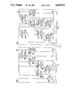
- an adder SM1 multiplies the first coefficient (18) in the right hand column of Table 3, and register RG11 memorizes the result.
- SM1 receives RG1 register output 3 (FIG. 1) shifted by 4 positions to the left at the first input and by 1 position at the second input (multiplications by 16 and 2).
- a subtractor ST1 multiplies the second coefficient (35), and register RG13 memorizes the result.
- ST1 subtracts output 3 applied to the first input from the RG11 output applied to the second input and shifted by one position to the left.
- An adder SM2 multiplies the third coefficient (50), and register RG12 memorizes the result.
- SM2 receives output 3 shifted to the left by 5 positions and the output of register RG11.
- a register RG17 multiplies the fourth and eight coefficient (64); in fact, it receives output 3 shifted by 6 positions.
- An adder SM4 multiplies the fifth coefficient (75), and a register RG16 memorizes the result.
- Adder SM4 receives register RG12 output shifted by one position to the right (division by 2) at the first input, and unshifted at the second input.
- a subtracter ST2 multiplies the sixth coefficient (84), and register RG14 memorizes the result.
- SM3 receives output 3 shifted by 6 positions to the left and the output of register RG12 shifted by 1 position to the right (division by 2).
- registers RG11, . . . , RG17 are brought to 7-input multiplexers MX5.
- Register RG17 output will be switched twice by multiplexer MX5 on output 5.
- an adder SM6 multiplies the first coefficient (9) in the left-hand column of Table 3, a register RG19 memorizes the result. SM6 receives output 4 shifted by 3 positions to the left at the first input, and unshifted at the second input.
- An adder SM7 multiplies the second coefficient (26), and register RG20 memorizes the result.
- Adder SM7 receives output 4 shifted by 3 positions to the left, and register RG19 output scaled by 1 position to the left.
- a subtracter ST4 multiplies the third coefficient (43) and register RG23 memorizes the result.
- Subtracter ST4 subtracts register RG19 output from register RG20 output shifted by one position to the left.
- a subtracter ST3 multiplies the fourth coefficient (-70) and register RG21 memorizes the result.
- ST3 subtracts register RG19 output shifted by 3 positions to the left from output 4 shifted by on position to the left. In this case, the coefficient sign makes no difference, as it does not influence circuit complication.
- An adder SM5 multiplies the fifth coefficient (80) and register RG18 memorizes the result.
- SM5 receives output 4 shifted by 6 positions to the left at the first input, and by 4 positions to the left at the second input.
- An adder SM9 multiplies the sixth coefficient (57) and register RG24 memorizes the result.
- SM9 receives register RG19 output shifted by 4 positions to the right (division by 16) and register RG20 output shifted by one position to the left.
- An adder SM10 multiplies the seventh coefficient (87) and register RG25 memorizes the result. SM10 receives output 4 unshifted and register RG23 shifted by one position to the left.
- An adder SM8 multiplies the eight coefficient (90) and register RG22 memorizes the result. SM8 receives output 4 scaled by six positions to the left, and register RG20 output unshifted.
- Outputs of registers RG18, . . . , RG25 are brought to 8 input multiplexer MX6.
- the addresser/controller ADR2 (FIG. 1) controls only multiplexers MX5 and MX6 by selecting, via connection 7 control signals, a suitable succession of input connections with outputs 5 and 6. It is not necessary to provide special loading commands for registers RG11, RG12, . . . RG25, as it is sufficient that data at their outputs be stable and correct at the time they are taken by multiplexers MX5 and MX6. Furthermore, data at register RG1 and RG2 outputs 3 and 4 (FIG. 1) remain fixed for the time required for circuits ERM and ORM to perform all calculations, i.e. the calcualtions relating to one transform coefficient matrix column. Consequently, it is sufficient to command register loading by means of the normal clock signal, which is brought to all circuit registers but is not shown in the figure for reasons of simplicity, and the various operation results propagate among the various cascade-connected register levels.
- the embodiment shown in fIG. 3 calls for the use of a larger number of components (or of equivalent logic gates if integrated circuits are employed) than the example shown in FIG. 2, but permits higher computing speeds and simplifies addressing by the ADR2 block.
- this circuit solution follows that shown in FIG. 2, the reader is directed to the description of said circuit for general considerations regarding components used, operation and ADR2 block control mode (FIG. 1).
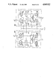
- the ERM block For each datum at inputs 3 and 4, the ERM block performs multiplications by the coefficients in the right hand column in Table 4, while ORM multiplies by the coefficients in the left hand column, proceeding from top to bottom of Table 4.
- the ERM block consists of two multiplexers MX7 and MX8, a barrel shifter SH5 downstream of MX4, a subtracter SMST5 which subtracts SH5 output from MX8 output, and two registers RG27 and RG28 which can memorize output 5 of SMST5.
- MX4 receives RG27 outputs 3 and 20; MX8 inuts reveice G27 outputs 3 and 20 and RG28 output 21.
- output 21 of register RG28 is applied to an MX8 input shifted by one position to the left (multiplication by 2 of coefficient 49 and 91); register RG27 output 20 and RG1 output 3 (FIG. 1) are applied to MX8 shifted by three positions to the left (multiplication by 8 of coefficient 7 and the input datum).
- multiplexers MX7 and MX8 are switched on input 3; shifter SH5 does not shift positions; adder/subtracter SMST5 output is stored in register RG27 and is not accumulated in memory MEM2 (FIG. 1) because it is used only inside the ERM block.
- multiplexers MX7 and MX8 are switched on register RG27 output 20; shifter SH5 does not shift positions; adder/subtracter SMST5 output is stored in register RG28 and is also taken from output 5 and accumulated in memory MEM2 (FIG. 1).
- multiplexer MX7 is switched on register RG27 output 20 and multiplexer MX8 is switched on regiser RG28 output 21, and shifter SH5 does not shift positions.
- the same cycle of operations is used for the fourth coefficient (91); at the end of the result of adder/subtracter SMST5 is also stored in register RG28.
- multiplexer MX7 is switched on output 3
- multiplexer MX8 is switched on register RG28 output 21
- shifter SH5 shifts by 6 positions to the left (multiplication by 64).
- the ORM block consists of two multiplexers MX9 and MX10 followed by two barrel-shifters SH6 and SH7 which feed an adder/subtracter SMST6 whose output 6 can also be stored in two registers RG29 and RG30.
- MX9 receives RG2 output 4 (FIG. 1) and register RG29 output 22, while multiplexer MX10 receives register RG30 outputs 4 and 33.
- multiplexers MX9 and MX10 are switched on register RG1 output 4 (FIG. 1); shifter SH6 does not shift; shifter SH7 shifts by three positions to the left; adder/subtracter SMST6 subtracts shifter SH6 output from shifter SH7 output; and adder/subtracter SMST6 output is only stoed in RG29, and is not accumulated in memory MEM2 (FIG. 1) because it is used only inside the ORM block.
- multiplexer MX9 is switched on register RG29 output 22, multiplexer MX10 is switched onoutput 4; shifter SH6 does not shift, while shifter SH7 shifts by five positions; adder/subtracter SMST6 subtracts shifter SH6 output from shifter SH7 output; and the output is also stored in register RG30.
- multiplexer MX9 is switched on register RG29 output 22, multiplexer MX10 is switched on output 4; shifter SH6 does not shift, while shifter SH7 shifts by six positions; and adder/subtracter SMST6 adds the outputs of shifters SH6 and SH7.
- multiplexer MX9 is switched on RG9 output 22, multiplexer MX10 is switched on register RG10 output 23; shifter SH6 shifts by 3 positions to the left and SH7 by one, and adder/subtracter SMST6 adds the outputs of shifters SH6 and SH7.
- multiplexers MX9 and MX10 are switched on output 4; shifter SH6 shifts by one position and shifter SH7 by seven positions to the left, and adder/subtracters SMST6 subtracts shifter SH6 output from shifter SH7 output.
- the ERM block For each datum at inputs 3 and 4, the ERM block performs multiplications by the coefficients in the right hand column on Table 4, while ORM multiplies by the coefficients in the left hand column of the Table.
- a subtracter ST6 multiplies the datum on register RG1 output 3 (FIG. 1) by the first coefficient (7), in the righthand column on Table 4, and the result is stored in register RG31.
- subtracter ST6 receives output 3, shifted by three positions to the left at the minuend input.
- a subtracter ST7 multiplies the second coefficient (49) and the result is stored in register RG32. At its two inputs, ST7 receives register RG31 output, shifted by three positions at the minuend input.
- a subtracter ST8 multiplies the third coefficient (91) and the result is stored in register RG33.
- ST8 subtracts RG31 output from register RG32 output shifted by one position to the left.
- a subtracters ST9 multiplies the fourth coefficient (118) and the result is stored in register RG34.
- ST9 subtracts output 3 shifted by six positions to the left register RG33 output shifted by one position to the left.
- Outputs of registers RG32, RG33 and RG34 are applied to the inputs of a 3-input multiplexer MX11, and are connected in turn to output 5; RG33 output is used twice.
- subtracter ST10 multiplies the datum on register RG2 output 4 (FIG. 1) for the first coefficient (7) in the left-hand column on Table 4, and the result is stored in register RG35.
- ST10 receives output 4 shifted by three positions to the left at the minuend input.
- a subtracter ST12 multiplies the second coefficient (25) and the result is stored in register RG37. ST12 subtracts RG35 output from output 4 shifted by five positions to the left.
- An adder SM12 multiplies the third coefficient (71), and the result is stored in register RG38. SM12 adds output 4 shifted by six positions to the left to register RG35 output.
- An adder SM13 multiplies the fourth coefficient (106), and the result is stored in a register RG39.
- Adder SM13 adds RG35 output shifted by three positions to the left with register RG37 output shifted by one position to the left.
- a subtracter ST11 multiplies the fifth coefficient (126), and register RG36 stores the result. At its two inputs, subtracter ST11 receives output 4, shifted by seven positions to the left at the minuend input, and by one position to the left at the subtrahend input.
- Outputs of registers RG36, RG37, RG38, and RG39 are applied to the inputs of a 4-input multiplexer MX12, and connected in turn to output 6.
- FIG. 5 calls for the use of a larger number of components (or of equivalent logic gates if integrated circuits are employed) than that of FIG. 4, but permits higher computing speeds and simplifies addressing by the ADR2 block.
- the circuit shown in FIG. 1 must thus be expanded to include memories for intermediate transform product accumulation and standard circuits for addressing said memories, which can also perform the functions of blocks MEM1 and ADR1 (FIG. 1).
- the circuit covered by this patent application can be advantageously embodied as a VLSI circuit. Supposing a representation precision of 12 bits for each input vector f(j) component and 8 bits for the matrix coefficients, the circuit's complexity can be evaluated for each of the variants described.
- ERM and ORM blocks embodied as shown in FIG. 2 the overall circuit requires around 3500 equivalent gates (for example, with HCMOS technology, each equivalent gate consists of four transistors), plus a 16 ⁇ 24 bit accumulation memory (MEM2 and MEM3 blocks, FIG. 1). This embodiment provides an execution time per each elementary operation of around 60 ns.
- ERM and ORM embodiments as shown in FIG. 3 the overall structure requires around 5800 equivalent gates and an equal accumulation memory, with execution time per elementary operation of around 20 ns.
- ERM and ORM embodiments as shown in FIGS. 3 and 4 require 2900 and 4000 equivalent gates respectively and an 8 ⁇ 23 bit accumulation memory; execution time per elementary operation are still 60 ns and 20 ns respectively.
- FIG. 6 shows an embodiment of a two-dimensional DCT transform computational circuit. It consists of two cascade-connected one-dimensional DCT transform computation circuits (as shown in FIG. 1), indicated as DCT1 and DCT2, with an interposed memory MEM4 for temporary storage of intermediate result vectors F(k).
- the ADR3 block generates read/write addresses for MEM4 and synchronizes address generators ADR1 and ADR2 (FIG. 1) for blocks DCT1 and DCT2.
- Memory MEM4 is matrix-structured so as to contain N vectors F(k) of N components each, and is read in orthogonal way to the direction in which it is written (read by columns and written by lines or vice versa).
- Embodying the circuit shown in FIG. 6 should not pose problems for technicians in the field, given the description of the circuit shown in FIG. 1.
Landscapes
- Physics & Mathematics (AREA)
- General Physics & Mathematics (AREA)
- Engineering & Computer Science (AREA)
- Theoretical Computer Science (AREA)
- Computational Mathematics (AREA)
- Mathematical Analysis (AREA)
- Mathematical Optimization (AREA)
- Pure & Applied Mathematics (AREA)
- Mathematical Physics (AREA)
- General Engineering & Computer Science (AREA)
- Data Mining & Analysis (AREA)
- Discrete Mathematics (AREA)
- Computing Systems (AREA)
- Algebra (AREA)
- Databases & Information Systems (AREA)
- Software Systems (AREA)
- Complex Calculations (AREA)
- Compression, Expansion, Code Conversion, And Decoders (AREA)
- Compression Or Coding Systems Of Tv Signals (AREA)
Applications Claiming Priority (2)
| Application Number | Priority Date | Filing Date | Title |
|---|---|---|---|
| IT8767032A IT1207346B (it) | 1987-01-20 | 1987-01-20 | Sformata coseno discreta a coeffi circuito per il calcolo della tra cienti quantizzati di campioni di segnale numerico |
| IT67032A/87 | 1987-01-20 |
Publications (1)
| Publication Number | Publication Date |
|---|---|
| US4849922A true US4849922A (en) | 1989-07-18 |
Family
ID=11299044
Family Applications (1)
| Application Number | Title | Priority Date | Filing Date |
|---|---|---|---|
| US07/131,833 Expired - Fee Related US4849922A (en) | 1987-01-20 | 1987-12-11 | Circuit for computing the quantized coefficient discrete cosine transform of digital signal samples |
Country Status (6)
| Country | Link |
|---|---|
| US (1) | US4849922A (fr) |
| EP (1) | EP0275979B1 (fr) |
| JP (1) | JPH0622033B2 (fr) |
| CA (1) | CA1281425C (fr) |
| DE (1) | DE3875979T2 (fr) |
| IT (1) | IT1207346B (fr) |
Cited By (26)
| Publication number | Priority date | Publication date | Assignee | Title |
|---|---|---|---|---|
| DE4038240A1 (de) * | 1989-12-01 | 1991-06-06 | Ricoh Kk | Prozessor zum durchfuehren einer orthogonaltransformation |
| US5053985A (en) * | 1989-10-19 | 1991-10-01 | Zoran Corporation | Recycling dct/idct integrated circuit apparatus using a single multiplier/accumulator and a single random access memory |
| US5197021A (en) * | 1989-07-13 | 1993-03-23 | Telettra-Telefonia Elettronica E Radio S.P.A. | System and circuit for the calculation of the bidimensional discrete transform |
| FR2683694A1 (fr) * | 1991-11-08 | 1993-05-14 | Matra Communication | Dispositif de codage de signal video a activite temporelle. |
| US5249146A (en) * | 1991-03-27 | 1993-09-28 | Mitsubishi Denki Kabushiki Kaisha | Dct/idct processor and data processing method |
| US5257213A (en) * | 1991-02-20 | 1993-10-26 | Samsung Electronics Co., Ltd. | Method and circuit for two-dimensional discrete cosine transform |
| US5291429A (en) * | 1991-03-08 | 1994-03-01 | Fujitsu Limited | Circuit for matrix calculation of discrete cosine transformation |
| US5339265A (en) * | 1992-08-31 | 1994-08-16 | University Of Maryland At College Park | Optimal unified architectures for the real-time computation of time-recursive discrete sinusoidal transforms |
| US5343501A (en) * | 1991-02-19 | 1994-08-30 | Matsushita Electric Industrial Co., Ltd. | Orthogonal transform apparatus for video signal processing |
| US5345408A (en) * | 1993-04-19 | 1994-09-06 | Gi Corporation | Inverse discrete cosine transform processor |
| US5359549A (en) * | 1989-12-01 | 1994-10-25 | Ricoh Company, Ltd. | Orthogonal transformation processor for compressing information |
| US5394349A (en) * | 1992-07-10 | 1995-02-28 | Xing Technology Corporation | Fast inverse discrete transform using subwords for decompression of information |
| US5477469A (en) * | 1992-11-12 | 1995-12-19 | Nec Corporation | Operation device and operation method for discrete cosine transform and inverse discrete cosine transform |
| US5479364A (en) * | 1992-06-26 | 1995-12-26 | Discovision Associates | Method and arrangement for transformation of signals from a frequency to a time domain |
| US5781239A (en) * | 1996-06-20 | 1998-07-14 | Lsi Logic Corporation | System and method for performing an optimized inverse discrete cosine transform with improved efficiency |
| US5784011A (en) * | 1996-06-14 | 1998-07-21 | Lsi Logic Corporation | Multiplier circuit for performing inverse quantization arithmetic |
| US5943502A (en) * | 1994-12-09 | 1999-08-24 | Neomagic Israel Ltd. | Apparatus and method for fast 1D DCT |
| US6217234B1 (en) | 1994-07-29 | 2001-04-17 | Discovision Associates | Apparatus and method for processing data with an arithmetic unit |
| US6356995B2 (en) * | 1998-07-02 | 2002-03-12 | Picoturbo, Inc. | Microcode scalable processor |
| WO2002035380A1 (fr) * | 2000-10-23 | 2002-05-02 | International Business Machines Corporation | Transformees plus rapides a termes avec echelle, suspensions anticipees et ameliorations de precision |
| US20020111978A1 (en) * | 2000-12-19 | 2002-08-15 | Philips Electronics North America Corporation | Approximate inverse discrete cosine transform for scalable computation complexity video and still image decoding |
| US6732131B1 (en) * | 1999-09-30 | 2004-05-04 | Kabushikikaisha Toshiba | Discrete cosine transformation apparatus, inverse discrete cosine transformation apparatus, and orthogonal transformation apparatus |
| US20040196824A1 (en) * | 2003-03-14 | 2004-10-07 | Thuyen Le | Device for synchronization of a mobile radio receiver to a frame structure of a received radio signal |
| US6895421B1 (en) * | 2000-10-06 | 2005-05-17 | Intel Corporation | Method and apparatus for effectively performing linear transformations |
| US20050171986A1 (en) * | 1999-12-10 | 2005-08-04 | Broadcom Corporation | Apparatus and method for reducing precision of data |
| USRE43248E1 (en) | 1994-06-10 | 2012-03-13 | Arm Limited | Interoperability with multiple instruction sets |
Families Citing this family (11)
| Publication number | Priority date | Publication date | Assignee | Title |
|---|---|---|---|---|
| US6336180B1 (en) | 1997-04-30 | 2002-01-01 | Canon Kabushiki Kaisha | Method, apparatus and system for managing virtual memory with virtual-physical mapping |
| FR2646046B1 (fr) * | 1989-04-18 | 1995-08-25 | France Etat | Procede et dispositif de compression de donnees d'image par transformation mathematique a cout reduit de mise en oeuvre, notamment pour la transmission a debit reduit de sequences d'images |
| US5689592A (en) * | 1993-12-22 | 1997-11-18 | Vivo Software, Inc. | Parallel processing of digital signals in a single arithmetic/logic unit |
| AT402586B (de) * | 1994-05-05 | 1997-06-25 | Siemens Ag Oesterreich | Verfahren zur durchführung der diskreten-kosinus-transformation |
| AUPO648397A0 (en) | 1997-04-30 | 1997-05-22 | Canon Information Systems Research Australia Pty Ltd | Improvements in multiprocessor architecture operation |
| US6414687B1 (en) | 1997-04-30 | 2002-07-02 | Canon Kabushiki Kaisha | Register setting-micro programming system |
| AUPO647997A0 (en) | 1997-04-30 | 1997-05-22 | Canon Information Systems Research Australia Pty Ltd | Memory controller architecture |
| US6507898B1 (en) | 1997-04-30 | 2003-01-14 | Canon Kabushiki Kaisha | Reconfigurable data cache controller |
| US6707463B1 (en) | 1997-04-30 | 2004-03-16 | Canon Kabushiki Kaisha | Data normalization technique |
| US6061749A (en) | 1997-04-30 | 2000-05-09 | Canon Kabushiki Kaisha | Transformation of a first dataword received from a FIFO into an input register and subsequent dataword from the FIFO into a normalized output dataword |
| CN107066234B (zh) * | 2017-04-21 | 2020-05-26 | 重庆邮电大学 | 一种量子乘法器的设计方法 |
Citations (6)
| Publication number | Priority date | Publication date | Assignee | Title |
|---|---|---|---|---|
| US4196448A (en) * | 1978-05-15 | 1980-04-01 | The United States Of America As Represented By The Secretary Of The Navy | TV bandwidth reduction system using a hybrid discrete cosine DPCM |
| US4293920A (en) * | 1979-09-04 | 1981-10-06 | Merola Pasquale A | Two-dimensional transform processor |
| US4385363A (en) * | 1978-12-15 | 1983-05-24 | Compression Labs, Inc. | Discrete cosine transformer |
| US4449194A (en) * | 1981-09-25 | 1984-05-15 | Motorola Inc. | Multiple point, discrete cosine processor |
| US4675836A (en) * | 1984-03-09 | 1987-06-23 | Compagnie Industrielle Des Telecommunications Cit-Alcatel | Discrete cosine transform calculation processor |
| US4679163A (en) * | 1984-03-09 | 1987-07-07 | Compagnie Industrielle Des Telecommunications Cit-Alcatel | Inverse discrete cosine transform calculation processor |
Family Cites Families (1)
| Publication number | Priority date | Publication date | Assignee | Title |
|---|---|---|---|---|
| US4562484A (en) * | 1983-08-19 | 1985-12-31 | Advanced Micro Devices, Inc. | Method and device for decoding two-dimensional facsimile signals |
-
1987
- 1987-01-20 IT IT8767032A patent/IT1207346B/it active
- 1987-12-11 US US07/131,833 patent/US4849922A/en not_active Expired - Fee Related
-
1988
- 1988-01-04 CA CA000555741A patent/CA1281425C/fr not_active Expired - Lifetime
- 1988-01-14 JP JP63005050A patent/JPH0622033B2/ja not_active Expired - Lifetime
- 1988-01-19 DE DE8888100692T patent/DE3875979T2/de not_active Expired - Fee Related
- 1988-01-19 EP EP88100692A patent/EP0275979B1/fr not_active Expired
Patent Citations (6)
| Publication number | Priority date | Publication date | Assignee | Title |
|---|---|---|---|---|
| US4196448A (en) * | 1978-05-15 | 1980-04-01 | The United States Of America As Represented By The Secretary Of The Navy | TV bandwidth reduction system using a hybrid discrete cosine DPCM |
| US4385363A (en) * | 1978-12-15 | 1983-05-24 | Compression Labs, Inc. | Discrete cosine transformer |
| US4293920A (en) * | 1979-09-04 | 1981-10-06 | Merola Pasquale A | Two-dimensional transform processor |
| US4449194A (en) * | 1981-09-25 | 1984-05-15 | Motorola Inc. | Multiple point, discrete cosine processor |
| US4675836A (en) * | 1984-03-09 | 1987-06-23 | Compagnie Industrielle Des Telecommunications Cit-Alcatel | Discrete cosine transform calculation processor |
| US4679163A (en) * | 1984-03-09 | 1987-07-07 | Compagnie Industrielle Des Telecommunications Cit-Alcatel | Inverse discrete cosine transform calculation processor |
Non-Patent Citations (6)
| Title |
|---|
| Hague, "A Two-Dimensional Fast Cosine Transform", IEEE Trans. on Acoustics, Speech, and Signal Processing, vol. ASSP-33, No. 6, 12/85, pp. 1532-1539. |
| Hague, A Two Dimensional Fast Cosine Transform , IEEE Trans. on Acoustics, Speech, and Signal Processing, vol. ASSP 33, No. 6, 12/85, pp. 1532 1539. * |
| Haralick, "A Storage Efficient Way to Implement the Discrete Cosine Transform", IEEE Trans. on Comp., Jul. 1976, pp. 764-765. |
| Haralick, A Storage Efficient Way to Implement the Discrete Cosine Transform , IEEE Trans. on Comp., Jul. 1976, pp. 764 765. * |
| Kamanger et al., "Fast Algorithms for the 2-D Discrete Cosine Transform", IEEE Trans. on Computers, vol. C-31, No. 9, Sep. 1982, pp. 899-906. |
| Kamanger et al., Fast Algorithms for the 2 D Discrete Cosine Transform , IEEE Trans. on Computers, vol. C 31, No. 9, Sep. 1982, pp. 899 906. * |
Cited By (33)
| Publication number | Priority date | Publication date | Assignee | Title |
|---|---|---|---|---|
| US5197021A (en) * | 1989-07-13 | 1993-03-23 | Telettra-Telefonia Elettronica E Radio S.P.A. | System and circuit for the calculation of the bidimensional discrete transform |
| US5053985A (en) * | 1989-10-19 | 1991-10-01 | Zoran Corporation | Recycling dct/idct integrated circuit apparatus using a single multiplier/accumulator and a single random access memory |
| US5359549A (en) * | 1989-12-01 | 1994-10-25 | Ricoh Company, Ltd. | Orthogonal transformation processor for compressing information |
| US5268853A (en) * | 1989-12-01 | 1993-12-07 | Ricoh Company, Ltd. | Orthogonal transformation processor for compressing information |
| US5331585A (en) * | 1989-12-01 | 1994-07-19 | Ricoh Company, Ltd. | Orthogonal transformation processor for compressing information |
| DE4038240A1 (de) * | 1989-12-01 | 1991-06-06 | Ricoh Kk | Prozessor zum durchfuehren einer orthogonaltransformation |
| US5343501A (en) * | 1991-02-19 | 1994-08-30 | Matsushita Electric Industrial Co., Ltd. | Orthogonal transform apparatus for video signal processing |
| US5257213A (en) * | 1991-02-20 | 1993-10-26 | Samsung Electronics Co., Ltd. | Method and circuit for two-dimensional discrete cosine transform |
| US5291429A (en) * | 1991-03-08 | 1994-03-01 | Fujitsu Limited | Circuit for matrix calculation of discrete cosine transformation |
| US5249146A (en) * | 1991-03-27 | 1993-09-28 | Mitsubishi Denki Kabushiki Kaisha | Dct/idct processor and data processing method |
| FR2683694A1 (fr) * | 1991-11-08 | 1993-05-14 | Matra Communication | Dispositif de codage de signal video a activite temporelle. |
| US5590067A (en) * | 1992-06-26 | 1996-12-31 | Discovision Associates | Method and arrangement for transformation of signals from a frequency to a time domain |
| US5479364A (en) * | 1992-06-26 | 1995-12-26 | Discovision Associates | Method and arrangement for transformation of signals from a frequency to a time domain |
| US5594678A (en) * | 1992-06-26 | 1997-01-14 | Discovision Associates | Method and arrangement for transformation of signals from a frequency to a time domain |
| US5394349A (en) * | 1992-07-10 | 1995-02-28 | Xing Technology Corporation | Fast inverse discrete transform using subwords for decompression of information |
| US5339265A (en) * | 1992-08-31 | 1994-08-16 | University Of Maryland At College Park | Optimal unified architectures for the real-time computation of time-recursive discrete sinusoidal transforms |
| US5477469A (en) * | 1992-11-12 | 1995-12-19 | Nec Corporation | Operation device and operation method for discrete cosine transform and inverse discrete cosine transform |
| US5345408A (en) * | 1993-04-19 | 1994-09-06 | Gi Corporation | Inverse discrete cosine transform processor |
| USRE43248E1 (en) | 1994-06-10 | 2012-03-13 | Arm Limited | Interoperability with multiple instruction sets |
| US6217234B1 (en) | 1994-07-29 | 2001-04-17 | Discovision Associates | Apparatus and method for processing data with an arithmetic unit |
| US5943502A (en) * | 1994-12-09 | 1999-08-24 | Neomagic Israel Ltd. | Apparatus and method for fast 1D DCT |
| US5784011A (en) * | 1996-06-14 | 1998-07-21 | Lsi Logic Corporation | Multiplier circuit for performing inverse quantization arithmetic |
| US5781239A (en) * | 1996-06-20 | 1998-07-14 | Lsi Logic Corporation | System and method for performing an optimized inverse discrete cosine transform with improved efficiency |
| US6356995B2 (en) * | 1998-07-02 | 2002-03-12 | Picoturbo, Inc. | Microcode scalable processor |
| US6732131B1 (en) * | 1999-09-30 | 2004-05-04 | Kabushikikaisha Toshiba | Discrete cosine transformation apparatus, inverse discrete cosine transformation apparatus, and orthogonal transformation apparatus |
| US20050171986A1 (en) * | 1999-12-10 | 2005-08-04 | Broadcom Corporation | Apparatus and method for reducing precision of data |
| US6895421B1 (en) * | 2000-10-06 | 2005-05-17 | Intel Corporation | Method and apparatus for effectively performing linear transformations |
| US7337204B2 (en) | 2000-10-06 | 2008-02-26 | Intel Corporation | Method and apparatus for effectively performing linear transformations |
| CN100429644C (zh) * | 2000-10-23 | 2008-10-29 | 国际商业机器公司 | 使用比例项、早期中止和精度细算的更快速变换 |
| WO2002035380A1 (fr) * | 2000-10-23 | 2002-05-02 | International Business Machines Corporation | Transformees plus rapides a termes avec echelle, suspensions anticipees et ameliorations de precision |
| US20020111978A1 (en) * | 2000-12-19 | 2002-08-15 | Philips Electronics North America Corporation | Approximate inverse discrete cosine transform for scalable computation complexity video and still image decoding |
| US6859815B2 (en) * | 2000-12-19 | 2005-02-22 | Koninklijke Philips Electronics N.V. | Approximate inverse discrete cosine transform for scalable computation complexity video and still image decoding |
| US20040196824A1 (en) * | 2003-03-14 | 2004-10-07 | Thuyen Le | Device for synchronization of a mobile radio receiver to a frame structure of a received radio signal |
Also Published As
| Publication number | Publication date |
|---|---|
| IT1207346B (it) | 1989-05-17 |
| EP0275979A3 (en) | 1989-11-02 |
| IT8767032A0 (it) | 1987-01-20 |
| DE3875979D1 (de) | 1992-12-24 |
| DE3875979T2 (de) | 1993-04-29 |
| EP0275979B1 (fr) | 1992-11-19 |
| CA1281425C (fr) | 1991-03-12 |
| EP0275979A2 (fr) | 1988-07-27 |
| JPH0622033B2 (ja) | 1994-03-23 |
| JPS63182773A (ja) | 1988-07-28 |
Similar Documents
| Publication | Publication Date | Title |
|---|---|---|
| US4849922A (en) | Circuit for computing the quantized coefficient discrete cosine transform of digital signal samples | |
| Madisetti et al. | A 100 MHz 2-D 8/spl times/8 DCT/IDCT processor for HDTV applications | |
| US6366936B1 (en) | Pipelined fast fourier transform (FFT) processor having convergent block floating point (CBFP) algorithm | |
| Swartzlander et al. | FFT implementation with fused floating-point operations | |
| Chan et al. | On the realization of discrete cosine transform using the distributed arithmetic | |
| US5197021A (en) | System and circuit for the calculation of the bidimensional discrete transform | |
| KR19990044304A (ko) | 압축 데이터 연산용 명령 세트 | |
| Sona et al. | Vedic multiplier implementation in VLSI | |
| US7020671B1 (en) | Implementation of an inverse discrete cosine transform using single instruction multiple data instructions | |
| Kammoun et al. | Hardware acceleration of approximate transform module for the versatile video coding standard | |
| Li et al. | An area-efficient large integer NTT-multiplier using discrete twiddle factor approach | |
| US6003058A (en) | Apparatus and methods for performing arithimetic operations on vectors and/or matrices | |
| JPH10504408A (ja) | 逆離散余弦変換を実行する装置および方法 | |
| Alam et al. | A new time distributed DCT architecture for MPEG-4 hardware reference model | |
| Pineiro et al. | High-radix logarithm with selection by rounding | |
| US5825420A (en) | Processor for performing two-dimensional inverse discrete cosine transform | |
| US5847980A (en) | Product-summing arithmetic circuit | |
| Villalba et al. | Radix-4 vectoring cordic algorithm and architectures | |
| Mehendale et al. | DA-based circuits for inner-product computation | |
| Bruguera et al. | 2-D DCT using on-line arithmetic | |
| US5999958A (en) | Device for computing discrete cosine transform and inverse discrete cosine transform | |
| Panda | Performance Analysis and Design of a Discreet Cosine Transform processor Using CORDIC algorithm | |
| KR100202567B1 (ko) | 고속 역이산 코사인변환 연산장치 | |
| Chen et al. | The IDCT processor on the adder-based distributed arithmetic | |
| Kwan et al. | Implementation of DSP-RAM: an architecture for parallel digital signal processing in memory |
Legal Events
| Date | Code | Title | Description |
|---|---|---|---|
| AS | Assignment |
Owner name: CSELT - CENTRO STUDI E LABORATORI TELECOMUNICAZION Free format text: ASSIGNMENT OF ASSIGNORS INTEREST.;ASSIGNOR:RIOLFO, BENEDETTO;REEL/FRAME:004806/0523 Effective date: 19871113 Owner name: CSELT - CENTRO STUDI E LABORATORI TELECOMUNICAZION Free format text: ASSIGNMENT OF ASSIGNORS INTEREST;ASSIGNOR:RIOLFO, BENEDETTO;REEL/FRAME:004806/0523 Effective date: 19871113 |
|
| FEPP | Fee payment procedure |
Free format text: PAYOR NUMBER ASSIGNED (ORIGINAL EVENT CODE: ASPN); ENTITY STATUS OF PATENT OWNER: LARGE ENTITY |
|
| FPAY | Fee payment |
Year of fee payment: 4 |
|
| REMI | Maintenance fee reminder mailed | ||
| LAPS | Lapse for failure to pay maintenance fees | ||
| FP | Lapsed due to failure to pay maintenance fee |
Effective date: 19970723 |
|
| STCH | Information on status: patent discontinuation |
Free format text: PATENT EXPIRED DUE TO NONPAYMENT OF MAINTENANCE FEES UNDER 37 CFR 1.362 |