US4900917A - Polarization insensitive optical communication device utilizing optical preamplification - Google Patents
Polarization insensitive optical communication device utilizing optical preamplification Download PDFInfo
- Publication number
- US4900917A US4900917A US07/219,684 US21968488A US4900917A US 4900917 A US4900917 A US 4900917A US 21968488 A US21968488 A US 21968488A US 4900917 A US4900917 A US 4900917A
- Authority
- US
- United States
- Prior art keywords
- optical
- polarization
- amplified
- signal
- component
- Prior art date
- Legal status (The legal status is an assumption and is not a legal conclusion. Google has not performed a legal analysis and makes no representation as to the accuracy of the status listed.)
- Expired - Lifetime
Links
Images

Classifications
-
- H—ELECTRICITY
- H04—ELECTRIC COMMUNICATION TECHNIQUE
- H04B—TRANSMISSION
- H04B10/00—Transmission systems employing electromagnetic waves other than radio-waves, e.g. infrared, visible or ultraviolet light, or employing corpuscular radiation, e.g. quantum communication
- H04B10/60—Receivers
- H04B10/66—Non-coherent receivers, e.g. using direct detection
- H04B10/67—Optical arrangements in the receiver
- H04B10/671—Optical arrangements in the receiver for controlling the input optical signal
- H04B10/672—Optical arrangements in the receiver for controlling the input optical signal for controlling the power of the input optical signal
- H04B10/673—Optical arrangements in the receiver for controlling the input optical signal for controlling the power of the input optical signal using an optical preamplifier
-
- H—ELECTRICITY
- H04—ELECTRIC COMMUNICATION TECHNIQUE
- H04B—TRANSMISSION
- H04B10/00—Transmission systems employing electromagnetic waves other than radio-waves, e.g. infrared, visible or ultraviolet light, or employing corpuscular radiation, e.g. quantum communication
- H04B10/27—Arrangements for networking
-
- H—ELECTRICITY
- H04—ELECTRIC COMMUNICATION TECHNIQUE
- H04B—TRANSMISSION
- H04B10/00—Transmission systems employing electromagnetic waves other than radio-waves, e.g. infrared, visible or ultraviolet light, or employing corpuscular radiation, e.g. quantum communication
- H04B10/27—Arrangements for networking
- H04B10/272—Star-type networks or tree-type networks
-
- H—ELECTRICITY
- H04—ELECTRIC COMMUNICATION TECHNIQUE
- H04B—TRANSMISSION
- H04B10/00—Transmission systems employing electromagnetic waves other than radio-waves, e.g. infrared, visible or ultraviolet light, or employing corpuscular radiation, e.g. quantum communication
- H04B10/60—Receivers
-
- H—ELECTRICITY
- H04—ELECTRIC COMMUNICATION TECHNIQUE
- H04B—TRANSMISSION
- H04B10/00—Transmission systems employing electromagnetic waves other than radio-waves, e.g. infrared, visible or ultraviolet light, or employing corpuscular radiation, e.g. quantum communication
- H04B10/60—Receivers
- H04B10/66—Non-coherent receivers, e.g. using direct detection
- H04B10/69—Electrical arrangements in the receiver
Definitions
- the present invention relates to a polarization insensitive optical communication device utilizing optical preamplification and, more particularly, to such a device which uses polarization diversity to provide improved optical amplification.
- a message signal originates from a semiconductor light emitting source, travels over a length of optical fiber, and impinges the active region of a semiconductor photodetector.
- this relatively simple system is satisfactory.
- bit rates >4 Gb/s, for example
- the coupling efficiency of the system degrades significantly, with a sensitivity of only -26 dBm at 8 Gb/s transmission (with a 10 -9 bit error rate (BER)).
- BER bit error rate
- Most high bit rate systems require a sensitivity of at least -32 dBm.
- a solution to this problem is to provide optical amplification at the input of the photodetector.
- preamplify the optical signal before it enters the photodiode preamplify the optical signal before it enters the photodiode.
- One method of achieving this preamplification is to transform the optical signal into an electrical form (with a conventional photodiode, for example), perform standard electrical amplification with any of the various methods well-known in the art, then reconvert the amplified electrical signal into an amplified optical signal at the input of the receiver photodiode.
- this is a workable solution.
- the need to perform these optical-electrical and electrical-optical conversions has been found to seriously degrade the quality of the message signal. Further, these systems often require rather sophisticated and expensive electrical components.
- a preferable solution is to perform optical amplification directly upon the message signal.
- conventional lasers may be used to perform this optical amplification.
- this is considered an improvement, there still exists a problem with these devices in that they are sensitive to the state of polarization of the incoming light signal.
- the TE and TM polarization states may exhibit a difference in gain of approximately 10 dB.
- Such a polarization dependence is undesirable for optical amplifiers utilized with installed optical fiber-based communication networks, where the polarization state of the message signal is at best unknown, and at worst varies as a function of time.
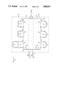
- FIG. 1 is a block diagram of an exemplary polarization insensitive arrangement of the present invention
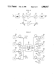
- FIG. 2 illustrates a polarization insensitive direct detection receiver utilizing the exemplary arrangement of FIG. 1;
- FIG. 3 illustrates an exemplary receiver configuration for use in the direct detection scheme of FIG. 2;
- FIG. 4 illustrates an exemplary in-line optical amplifier utilizing the arrangement of FIG. 1;
- FIG. 5 illustrates a wavelength division multiplexer (WDM) coherent communication scheme utilizing the in-line optical amplifier of FIG. 4.
- WDM wavelength division multiplexer
- FIG. 1 A simplified block diagram of the proposed polarization insensitive scheme of the present invention is illustrated in FIG. 1.
- an incoming optical signal I IN with an unknown polarization state is applied as an input to a polarization beam splitter 10 which functions to split signal I IN into two separate components having known polarizations.
- polarization beam splitter 10 functions to form a first component consisting of a TE polarized signal, denoted I TE , and a second component consisting of a TM polarized signal, denoted I TM .
- Polarization beam splitter 10 subsequently directs the first component I TE into a first section 12 of a polarization maintaining waveguide (polarization maintaining fiber, for example) and the second component I TM into a second section 14 of polarization maintaining waveguide.
- a polarization maintaining waveguide polarization maintaining fiber, for example
- the component propagating along waveguide section 12 will always be of a first, known state (TE) and similarly, the component propagating along waveguide section 14 will always be of the orthogonal state (TM).
- second component I TM is also amplified.
- second component I TM is redirected 90° by a mirror element 18 into a second optical amplifier 20.
- a laser amplifier will exhibit the most gain when the incoming signal is polarized along the TE axis.
- second laser amplifier 20 is oriented such that its TE axis is orthogonal to the direction of propagation of second component I TM and parallel to the electric field vector of second component I TM .
- the gain G 1 of first amplifier 16 be identical to the gain G 2 of second amplifier 20. This requirement is relatively easy to accomplish when the amplifiers are simultaneously fabricated on the same substrate. When this is the case, the gains will be relatively identical and will track each other as a function of both temperature and time. Otherwise, the DC drive currents applied to lasers 16 and 20 may be individually adjusted to equalize their gain.
- first component I' TE is directed along a waveguide 22 into a combiner element 26.
- second component I' TM is directed along a waveguide 24 into combiner element 26.
- combiner 26 performs either an electrical recombination of components I' TE and I' TM so as to form an electrical voltage output signal V OUT , or an optical recombination of components I' TE and I' TM so as to form an optical output signal I OUT .
- An optical recombination is performed when the arrangement of FIG. 1 is utilized as an in-line optical amplifier (for either direct detection or coherent communication systems), as discussed in association with FIGS. 4 and 5.
- an electrical recombination is performed when the arrangement of FIG. 1 is utilized as the receiver portion of a direct detection communication system, as discussed in detail below in association with FIGS. 2 and 3.
- first optical amplifier 16 and second optical amplifier 20 may be degraded by reflections as discussed in the O'Mahony article mentioned above. Such reflections may be caused by imperfect performance of polarization beam splitter 10, polarization maintaining waveguides 12, 14, 22 and 24 or mirror element 18. Such reflections may also be caused by imperfect performance of optical components prior to polarization beam splitter 10, or subsequent to combiner 26 when optical recombination is employed.
- isolators may be employed. Faraday optical isolators are known in the art as exemplary devices capable of performing optical isolation.
- the isolators may be fabricated using either bulk optics or integrated optics techniques.
- the need for optical isolators, the number and specific design of isolators to be employed and the location of such isolators with respect to optical amplifiers 16,20 will be apparent to those skilled in the art.
- FIG. 2 An exemplary direct detection receiver 30 utilizing the arrangement of FIG. 1 is illustrated in FIG. 2.
- the input to receiver 30 is an optical signal I IN comprising an unknown (and usually varying with time) polarization state.
- This signal is first applied as an input to polarization beam splitter 10 which functions as described above to separate I IN into two components of known, orthogonal polarizations, I TE and I TM .
- First component I TE as shown in FIG. 2, follows along branch 1 and is coupled into a polarization maintaining waveguide, illustrated in this embodiment as a section of polarization maintaining fiber 120, where fiber 120 directs component I TE into first laser amplifier 16.
- signal component I TM is coupled into a section of polarization maintaining fiber 140 and subsequently applied as an input to second laser amplifier 20.
- signal component I TM is coupled into a section of polarization maintaining fiber 140 and subsequently applied as an input to second laser amplifier 20.
- various lensing arrangements may be used to couple polarization maintaining fibers 120,140 to amplifiers 16,20, and that polarization maintaining waveguides of other forms could be utilized, where in some embodiments a reflecting element, such as mirror 18 of FIG. 1, would be required to redirect one of the signal components into its associated laser amplifier.
- bandpass filters may be placed at the exit of such amplifiers to minimize this noise factor.
- amplified signal I' TE exiting first laser amplifier 16 is subsequently applied as an input to a first optical bandpass filter 32.
- First filter 32 is chosen to comprise a sufficiently narrow bandwidth such that most of the spontaneous-spontaneous beat noise associated with the performance of laser amplifier 16 is removed from amplified signal I' TE .
- a second optical bandpass filter 34 is positioned at the exit of second laser amplifier 20 so as to perform the same function on amplified signal I' TM . It is to be understood that such filtering is not essential to the performance of receiver 30, but merely improves the quality of the final output signal.
- filtered signal I' TE travels along a section of polarization maintaining fiber 36 and is applied as an input to a first PIN-FET receiver 38.
- filtered signal I TE ' is coupled into the active region of a first PIN photodiode 40 which then transforms the optical signal into an equivalent voltage signal, denoted V 1 .
- Voltage signal V 1 is subsequently applied as an input to a conventional FET amplifying section 42 which is designed to provide a predetermined amount of signal gain.
- Filtered signal I' TM simultaneously propagates along a section of polarization maintaining fiber 44 and is applied as an input to a second PIN-FET receiveier 46.
- Second receiver 46 comprises a PIN photodiode 48 which is responsive to filtered signal I' TM to form an equivalent voltage representation denoted V 2 .
- Voltage signal V 2 is then applied as an input to FET amplifier 50, identical in form and function to FET amplifier 42.
- An exemplary matched amplifying section 42,50 will be described in detail in association with FIG. 3.
- First PIN-FET receiver 38 thus produces as an output a first amplified voltage signal V' 1 , which is representative of the TE polarized portion of the received light signal I IN .
- PIN-FET receiver 42 produces as an output a second amplified voltage signal V' 2 which is representative of the TM polarized portion of the received light signal I IN .
- receiver output signals V' 1 and V' 2 are applied as inputs to an electrical summing network, which may simply be a resistor bridge 52 as illustrated in FIG. 2.
- direct detection receiver 30 may be formed with either discrete components, or integrated to form a monolithic structure. A combination of these techniques may also be applied to form a hybrid arrangement.
- a discrete component version is relatively simple to envision, utilizing bulk optics to form polarization beam splitter 10 and filters 32,24; discrete semiconductor devices for laser amplifiers 16,20 and photodiodes 40,48; polarization maintaining optical fiber for the optical signal paths; and integrated (or discrete) electronic components for FET amplifiers 42,50 and summing network 52.
- receiver 30 may be of monolithic form, utilizing an optical substrate with polarization beam splitter 10, the various polarization maintaining waveguides, and filters 32,34 directly formed in the substrate material. Lasers 16,20, as well as PIN-FET receivers 38,42 may then be fabricated on this substrate, where various techniques for forming integrated opto-electronic devices are becoming utilized in the art.
- Operation of receiver 30 may be understood by considering baseband signal and noise currents for a given received optical power P of input signal I IN .
- a predetermined fraction kxP will be coupled into branch 1 associated with the amplification of signal I TE , where k is defined as the loss associated with a conventional polarization beam splitter and has been determined experimentally to be approximately equal to 0.71.
- the variable x is associated with the variation in the polarization of signal I IN (0 ⁇ x ⁇ 1, i.e., fully TE polarized through mixed polarizations to fully TM polarized).
- the optical power coupled into branch 2 associated with the amplification of signal I TM will thus be k(1-x)P.
- the baseband signal current associated with I IN may then be written as: ##EQU1## where the subscripts 1 and 2 refer to branches 1 and 2, hv is the photon energy, e the electronic charge, ⁇ is the photodiode quantum efficiency, G is defined as the laser amplifier gain, and ⁇ in , ⁇ out are the laser amplifier input and output coupling efficiencies, respectively.
- the photodetectors employed in the first detection receiver of the present invention are preferably matched devices. That is, the photodetectors exhibit like characteristics in terms of gain, efficiency, etc.
- the coupling arrangement i.e., lenses
- FIG. 3 An exemplary balanced receiver circuit 60 for converting the polarized light signals into the final receiver output V OUT is illustrated in FIG. 3.
- This particular arrangement is a three-stage FET amplifier which provides an overall transimpedance of approximately 1K ⁇ .
- first current signal I 1 provided by PIN 40 is first filtered by a simple RC network and passed through a blocking diode 62.
- Current signal I 1 is then applied as an input to a first amplifying stage 64, where stage 64 includes an FET 66 and associated resistive and capacitive elements. The specific values for these elements are chosen to provide the desired amount of voltage gain for first stage 64.
- first stage 64 is then applied as an input to a second amplifying stage 68, where a capacitor 70 is utilized to provide the AC coupling between first stage 64 and second stage 68.
- second stage 68 comprises an FET amplifying element, with various resistive and capacitive elements included to provide the predetermined amount of gain.
- the output of second stage 68 is then capacitively coupled via element 72 to a third amplifying stage 74.
- Third stage 74 also includes an FET amplifying element and the necessary resistive and capacitive elements.
- the output from third stage 76 is defined as the amplified voltage signal V' 1 and is AC coupled by a capacitor 76 to an input of resistor bridging network 52, as described above in association with FIG. 2.
- Second current signal I 2 provided by PIN photodiode 48 in response to light signal I' TM , follows a similar path through receiver 60.
- second current signal I 2 is first filtered and pressed through a second blocking diode 78.
- the signal then passes through a series of three amplifying stages 80, 82 and 84, each identical in form and function to those associated with signal I 1 as described above.
- the output from the last amplifying stage 84 is thus the amplified voltage signal V' 2 which is coupled by a capacitor 86 to another input of resistor bridging network 52.
- bridging network 52 functions to electrically sum the signals V' 1 and V' 2 to form the output signal V OUT .
- FIG. 4 A block diagram of one such exemplary in-line optical amplifier 90 is illustrated in FIG. 4.
- the input to such an amplifier 90 is an optical signal I IN comprising an unknown (and usually varying with time) polarization state.
- Input signal I IN is applied as an input to polarization beam splitter 10 which then breaks signal I IN into a pair of orthogonal components of known TE and TM polarization, the components being thus defined as I TE and I TM , respectively.
- first component I TE is subsequently applied as an input to first laser amplifier 16, where maximum coupling efficiency is achieved by aligning the TE axis of laser amplifier 16 with the electric field vector of signal I TE .
- second component I TM is applied as an input to second amplifier 20 which is aligned such that its TE axis is orthogonal to the direction of propagation of second component I TM and parallel to the electric field vector of second component I TM so as to provide maximum gain.
- second polarization beam splitter 92 is shown as being aligned with first optical amplifier 16 so that amplified signal I' TE may follow a direct path to the input of splitter 92. Therefore, amplified signal I' TM from second optical amplifier 20 must be redirected by a second reflecting surface 94 towards the remaining input of splitter 92. It is to be understood that polarization beam splitter 92 may also be positioned in the path of second amplifier 20, with signal I' TE being redirected towards an input to splitter 92.
- a pair of optical isolators 96 and 98 may be included with in-line amplifier 90 to prevent any reflected signal components (from various couplings, for example) from entering laser amplifiers 16 and 20, where these reflected signals would add destructively to the message signal, degrading the quality of output signal I OUT .
- Faraday optical isolators are known in the art as an exemplary device capable of performing optical isolation.
- an advantage of an in-line optical amplifier is that it may be used with a wavelength division multiplexed (VDM) coherent (or direct) detection communications network so as to provide amplification of each signal being transmitted, regardless of its operating wavelength.
- VDM wavelength division multiplexed
- WDM systems which utilize electrical amplification require separate amplifying units for each wavelength.
- a system utilizing the polarization insensitive in-line optical amplifier of the present invention will realize an approximate N-fold saving in amplifying components for an N signal system.
- FIG. 5 A simplified block diagram illustrating one such WDM system is illustrated in FIG. 5. As shown, the WDM system comprises a plurality of N transmitting units, denoted 100 1 -100 N , where each transmitter produces a separate message signal utilizing an assigned wavelength ⁇ 1 - ⁇ N .
Landscapes
- Engineering & Computer Science (AREA)
- Physics & Mathematics (AREA)
- Electromagnetism (AREA)
- Computer Networks & Wireless Communication (AREA)
- Signal Processing (AREA)
- Computing Systems (AREA)
- Optical Communication System (AREA)
Priority Applications (4)
| Application Number | Priority Date | Filing Date | Title |
|---|---|---|---|
| US07/219,684 US4900917A (en) | 1988-07-15 | 1988-07-15 | Polarization insensitive optical communication device utilizing optical preamplification |
| EP19890306857 EP0351133A3 (fr) | 1988-07-15 | 1989-07-06 | Dispositif de communication optique insensible à la polarisation utilisant une amplification optique préalable |
| JP1180642A JPH02134624A (ja) | 1988-07-15 | 1989-07-14 | 光学プリ増幅を使用する偏波インセンシティブ光学通信デバイス |
| CA000605666A CA1293997C (fr) | 1988-07-15 | 1989-07-14 | Dispositif de communication optique insensible a la polarisation utilisant une pre-amplification optique |
Applications Claiming Priority (1)
| Application Number | Priority Date | Filing Date | Title |
|---|---|---|---|
| US07/219,684 US4900917A (en) | 1988-07-15 | 1988-07-15 | Polarization insensitive optical communication device utilizing optical preamplification |
Publications (1)
| Publication Number | Publication Date |
|---|---|
| US4900917A true US4900917A (en) | 1990-02-13 |
Family
ID=22820315
Family Applications (1)
| Application Number | Title | Priority Date | Filing Date |
|---|---|---|---|
| US07/219,684 Expired - Lifetime US4900917A (en) | 1988-07-15 | 1988-07-15 | Polarization insensitive optical communication device utilizing optical preamplification |
Country Status (4)
| Country | Link |
|---|---|
| US (1) | US4900917A (fr) |
| EP (1) | EP0351133A3 (fr) |
| JP (1) | JPH02134624A (fr) |
| CA (1) | CA1293997C (fr) |
Cited By (21)
| Publication number | Priority date | Publication date | Assignee | Title |
|---|---|---|---|---|
| US5058103A (en) * | 1988-11-08 | 1991-10-15 | Fujitsu Limited | Bidirectional optical transmission system having a light-interruption detecting function |
| US5060301A (en) * | 1989-08-07 | 1991-10-22 | Oki Electric Industry Co., Ltd. | Optical repeated transmission method and system |
| US5204923A (en) * | 1989-07-17 | 1993-04-20 | Pirelli Cavi S.P.A. | Unit for amplifying light signals in optical fiber transmission lines |
| US5210808A (en) * | 1989-07-17 | 1993-05-11 | Pirelli Cavi S.P.A. | Unit for amplifying light signals in optical fiber transmission lines |
| US5258615A (en) * | 1990-08-03 | 1993-11-02 | Gpt Limited | Optical fiber monitoring by detection of polarization variations |
| US5295016A (en) * | 1991-07-15 | 1994-03-15 | Koninklijke Ptt Nederland, N.V. | Polarization insensitive amplification device |
| US5325226A (en) * | 1989-02-17 | 1994-06-28 | U.S. Philips Corporation | Optical coherent receiver |
| US5400164A (en) * | 1993-09-10 | 1995-03-21 | At&T Corp. | Polarization-insensitive optical four-photon mixer |
| USRE35697E (en) * | 1990-07-16 | 1997-12-23 | Pirelli Cavi S.P.A. | Unit for amplifying light signals in optical fiber transmission lines |
| US6271948B1 (en) * | 1997-05-16 | 2001-08-07 | Nec Corporation | Wavelength division multiplexed optical communication system |
| US6611369B2 (en) * | 1999-09-06 | 2003-08-26 | Furukawa Electric Co., Ltd. | Optical signal amplifier |
| US6636344B2 (en) * | 1998-07-23 | 2003-10-21 | The Furukawa Electric Co., Ltd. | Raman amplifier, optical repeater, and raman amplification method |
| US20040101313A1 (en) * | 2002-11-21 | 2004-05-27 | Fujitsu Limited | Optical repeater |
| US20040201882A1 (en) * | 2001-01-29 | 2004-10-14 | Nobuhiko Kikuchi | Optical amplifiers, optical fiber raman amplifiers and optical systems |
| US8736381B2 (en) * | 2012-10-12 | 2014-05-27 | Schneider Electric Industries Sas | Detection device provided with a transimpedance circuit |
| US20140348515A1 (en) * | 2011-12-15 | 2014-11-27 | Nec Corporation | Optical receiver and method for controlling optical receiver |
| US9647426B1 (en) * | 2013-06-28 | 2017-05-09 | Aurrion, Inc. | Polarization insensitive colorless optical devices |
| US20170230337A1 (en) * | 2016-02-05 | 2017-08-10 | Huawei Technologies Co., Ltd. | System and method for generating an obfuscated optical signal |
| CN111900610A (zh) * | 2020-07-30 | 2020-11-06 | 苏州长光华芯光电技术有限公司 | 一种激光光能回收装置及方法 |
| CN114415295A (zh) * | 2022-01-17 | 2022-04-29 | 成都市德科立菁锐光电子技术有限公司 | 发射光器件、光模块及提高光功率的方法 |
| US11646802B2 (en) | 2020-06-02 | 2023-05-09 | Hewlett Packard Enterprise Development Lp | Polarization independent optical receiver |
Families Citing this family (1)
| Publication number | Priority date | Publication date | Assignee | Title |
|---|---|---|---|---|
| US7433117B2 (en) * | 2004-04-30 | 2008-10-07 | Lucent Technologies Inc. | Polarization-diverse optical amplification |
Citations (10)
| Publication number | Priority date | Publication date | Assignee | Title |
|---|---|---|---|---|
| US3722982A (en) * | 1971-10-26 | 1973-03-27 | Westinghouse Electric Corp | Coherent optical processing method and system having improved signal-to-noise ratio utilizing polarizing filters |
| US3971930A (en) * | 1974-04-24 | 1976-07-27 | The United States Of America As Represented By The Administrator Of The National Aeronautics And Space Administration | Polarization compensator for optical communications |
| JPS60127A (ja) * | 1983-06-15 | 1985-01-05 | Fujitsu Ltd | デイジタル無線通信方式 |
| US4506388A (en) * | 1981-11-26 | 1985-03-19 | Michel Monerie | Process and apparatus for the coherent detection and demodulation of a phase-modulated carrier wave in a random polarization state |
| DE3431896A1 (de) * | 1984-08-30 | 1986-03-13 | Philips Patentverwaltung Gmbh, 2000 Hamburg | Verfahren zur korrektur der signalamplitude optischer nachrichtenempfaenger |
| US4635246A (en) * | 1983-10-20 | 1987-01-06 | The United States Of America As Represented By The Secretary Of The Navy | Frequency multiplex system using injection locking of multiple laser diodes |
| EP0251062A2 (fr) * | 1986-06-20 | 1988-01-07 | Fujitsu Limited | Récepteur pour signaux optiques doublement symétrique |
| US4752120A (en) * | 1985-03-18 | 1988-06-21 | Nec Corporation | Polarization controlling device comprising a beam splitter for controllably bifurcating an input polarized beam to two polarization controlling elements |
| US4777358A (en) * | 1987-03-30 | 1988-10-11 | Geo-Centers, Inc. | Optical differential strain gauge |
| US4778238A (en) * | 1985-08-01 | 1988-10-18 | Hicks John W | Optical communications systems and process for signal amplification using stimulated brillouin scattering (SBS) and laser utilized in the system |
Family Cites Families (6)
| Publication number | Priority date | Publication date | Assignee | Title |
|---|---|---|---|---|
| GB2167259B (en) * | 1984-11-21 | 1988-02-10 | Stc Plc | Optical fibre receiver |
| GB2172164B (en) * | 1985-03-07 | 1989-02-22 | Stc Plc | Balanced coherent receiver |
| JPS6319631A (ja) * | 1986-07-14 | 1988-01-27 | Furukawa Electric Co Ltd:The | 光信号の増幅方法 |
| GB2199713A (en) * | 1986-12-31 | 1988-07-13 | Stc Plc | Optical communication system |
| JPS63311331A (ja) * | 1987-06-15 | 1988-12-20 | Nippon Telegr & Teleph Corp <Ntt> | 光増幅装置 |
| JPS6426826A (en) * | 1987-07-23 | 1989-01-30 | Kokusai Denshin Denwa Co Ltd | Optical amplification system |
-
1988
- 1988-07-15 US US07/219,684 patent/US4900917A/en not_active Expired - Lifetime
-
1989
- 1989-07-06 EP EP19890306857 patent/EP0351133A3/fr not_active Withdrawn
- 1989-07-14 CA CA000605666A patent/CA1293997C/fr not_active Expired - Lifetime
- 1989-07-14 JP JP1180642A patent/JPH02134624A/ja active Pending
Patent Citations (10)
| Publication number | Priority date | Publication date | Assignee | Title |
|---|---|---|---|---|
| US3722982A (en) * | 1971-10-26 | 1973-03-27 | Westinghouse Electric Corp | Coherent optical processing method and system having improved signal-to-noise ratio utilizing polarizing filters |
| US3971930A (en) * | 1974-04-24 | 1976-07-27 | The United States Of America As Represented By The Administrator Of The National Aeronautics And Space Administration | Polarization compensator for optical communications |
| US4506388A (en) * | 1981-11-26 | 1985-03-19 | Michel Monerie | Process and apparatus for the coherent detection and demodulation of a phase-modulated carrier wave in a random polarization state |
| JPS60127A (ja) * | 1983-06-15 | 1985-01-05 | Fujitsu Ltd | デイジタル無線通信方式 |
| US4635246A (en) * | 1983-10-20 | 1987-01-06 | The United States Of America As Represented By The Secretary Of The Navy | Frequency multiplex system using injection locking of multiple laser diodes |
| DE3431896A1 (de) * | 1984-08-30 | 1986-03-13 | Philips Patentverwaltung Gmbh, 2000 Hamburg | Verfahren zur korrektur der signalamplitude optischer nachrichtenempfaenger |
| US4752120A (en) * | 1985-03-18 | 1988-06-21 | Nec Corporation | Polarization controlling device comprising a beam splitter for controllably bifurcating an input polarized beam to two polarization controlling elements |
| US4778238A (en) * | 1985-08-01 | 1988-10-18 | Hicks John W | Optical communications systems and process for signal amplification using stimulated brillouin scattering (SBS) and laser utilized in the system |
| EP0251062A2 (fr) * | 1986-06-20 | 1988-01-07 | Fujitsu Limited | Récepteur pour signaux optiques doublement symétrique |
| US4777358A (en) * | 1987-03-30 | 1988-10-11 | Geo-Centers, Inc. | Optical differential strain gauge |
Non-Patent Citations (2)
| Title |
|---|
| Wideband 1.5 um Optical Receiver Using Travelling Wave Laser Amplifier, M. J. O Mahony, I. W. Marshall, H. J. Westlake, W. G. Stallard, Electronics Letters, 6 Nov. 1986, vol. 22, No. 23. * |
| Wideband 1.5 um Optical Receiver Using Travelling-Wave Laser Amplifier, M. J. O'Mahony, I. W. Marshall, H. J. Westlake, W. G. Stallard, Electronics Letters, 6 Nov. 1986, vol. 22, No. 23. |
Cited By (41)
| Publication number | Priority date | Publication date | Assignee | Title |
|---|---|---|---|---|
| US5058103A (en) * | 1988-11-08 | 1991-10-15 | Fujitsu Limited | Bidirectional optical transmission system having a light-interruption detecting function |
| US5325226A (en) * | 1989-02-17 | 1994-06-28 | U.S. Philips Corporation | Optical coherent receiver |
| US5204923A (en) * | 1989-07-17 | 1993-04-20 | Pirelli Cavi S.P.A. | Unit for amplifying light signals in optical fiber transmission lines |
| US5210808A (en) * | 1989-07-17 | 1993-05-11 | Pirelli Cavi S.P.A. | Unit for amplifying light signals in optical fiber transmission lines |
| US5060301A (en) * | 1989-08-07 | 1991-10-22 | Oki Electric Industry Co., Ltd. | Optical repeated transmission method and system |
| USRE35697E (en) * | 1990-07-16 | 1997-12-23 | Pirelli Cavi S.P.A. | Unit for amplifying light signals in optical fiber transmission lines |
| US5258615A (en) * | 1990-08-03 | 1993-11-02 | Gpt Limited | Optical fiber monitoring by detection of polarization variations |
| US5295016A (en) * | 1991-07-15 | 1994-03-15 | Koninklijke Ptt Nederland, N.V. | Polarization insensitive amplification device |
| US5400164A (en) * | 1993-09-10 | 1995-03-21 | At&T Corp. | Polarization-insensitive optical four-photon mixer |
| AU675566B2 (en) * | 1993-09-10 | 1997-02-06 | At & T Corporation | Polarization-insensitive optical four-photon mixer |
| US6271948B1 (en) * | 1997-05-16 | 2001-08-07 | Nec Corporation | Wavelength division multiplexed optical communication system |
| US20070247701A1 (en) * | 1998-07-23 | 2007-10-25 | The Furukawa Electric Co., Ltd. | Raman amplifier, optical repeater, and raman amplification method |
| US7692852B2 (en) | 1998-07-23 | 2010-04-06 | The Furukawa Electric Co., Ltd. | Raman amplifier, optical repeater, and Raman amplification method |
| US6654162B2 (en) * | 1998-07-23 | 2003-11-25 | The Furukawa Electric Co., Ltd. | Raman amplifier, optical repeater, and Raman amplification method |
| US9281654B2 (en) | 1998-07-23 | 2016-03-08 | Furukawa Electric Co., Ltd. | Raman amplifier, optical repeater, and Raman amplification method |
| US6775057B2 (en) * | 1998-07-23 | 2004-08-10 | The Furukawa Electric Co., Ltd. | Raman amplifier, optical repeater, and raman amplification method |
| US20040190909A1 (en) * | 1998-07-23 | 2004-09-30 | The Furukawa Electric Co., Ltd. | Raman amplifier, optical repeater, and raman amplification method |
| US8437074B2 (en) | 1998-07-23 | 2013-05-07 | Furukawa Electric Co., Ltd. | Raman amplifier, optical repeater, and Raman amplification method |
| US6636344B2 (en) * | 1998-07-23 | 2003-10-21 | The Furukawa Electric Co., Ltd. | Raman amplifier, optical repeater, and raman amplification method |
| US20110141553A1 (en) * | 1998-07-23 | 2011-06-16 | Furukawa Electric Co., Ltd. | Raman amplifier, optical repeater, and raman amplification method |
| US7548368B2 (en) | 1998-07-23 | 2009-06-16 | The Furukawa Electric Co., Ltd. | Raman amplifier, optical repeater, and raman amplification method |
| US20040109230A1 (en) * | 1999-09-06 | 2004-06-10 | The Furukawa Electric Co., Ltd. | Optical signal amplifier |
| US6611369B2 (en) * | 1999-09-06 | 2003-08-26 | Furukawa Electric Co., Ltd. | Optical signal amplifier |
| US7400442B2 (en) | 1999-09-06 | 2008-07-15 | The Furukawa Electric Co., Ltd. | Optical signal amplifier |
| US6891659B2 (en) * | 2001-01-29 | 2005-05-10 | Hitachi, Ltd. | Optical amplifiers, optical fiber raman amplifiers and optical systems |
| US20040201882A1 (en) * | 2001-01-29 | 2004-10-14 | Nobuhiko Kikuchi | Optical amplifiers, optical fiber raman amplifiers and optical systems |
| US7375878B2 (en) * | 2002-11-21 | 2008-05-20 | Fujitsu Limited | Optical repeater |
| US20040101313A1 (en) * | 2002-11-21 | 2004-05-27 | Fujitsu Limited | Optical repeater |
| US7616377B2 (en) | 2002-11-21 | 2009-11-10 | Fujitsu Limited | Optical repeater |
| US20140348515A1 (en) * | 2011-12-15 | 2014-11-27 | Nec Corporation | Optical receiver and method for controlling optical receiver |
| US8736381B2 (en) * | 2012-10-12 | 2014-05-27 | Schneider Electric Industries Sas | Detection device provided with a transimpedance circuit |
| US10756516B2 (en) * | 2013-06-28 | 2020-08-25 | Aurrion, Inc. | Polarization insensitive colorless optical devices |
| US9647426B1 (en) * | 2013-06-28 | 2017-05-09 | Aurrion, Inc. | Polarization insensitive colorless optical devices |
| US11437786B2 (en) * | 2013-06-28 | 2022-09-06 | Openlight Photonics, Inc. | Polarization insensitive colorless optical devices |
| US10468854B1 (en) * | 2013-06-28 | 2019-11-05 | Aurrion, Inc. | Polarization insensitive colorless optical devices |
| US20190393681A1 (en) * | 2013-06-28 | 2019-12-26 | Aurrion, Inc. | Polarization insensitive colorless optical devices |
| US10397190B2 (en) * | 2016-02-05 | 2019-08-27 | Huawei Technologies Co., Ltd. | System and method for generating an obfuscated optical signal |
| US20170230337A1 (en) * | 2016-02-05 | 2017-08-10 | Huawei Technologies Co., Ltd. | System and method for generating an obfuscated optical signal |
| US11646802B2 (en) | 2020-06-02 | 2023-05-09 | Hewlett Packard Enterprise Development Lp | Polarization independent optical receiver |
| CN111900610A (zh) * | 2020-07-30 | 2020-11-06 | 苏州长光华芯光电技术有限公司 | 一种激光光能回收装置及方法 |
| CN114415295A (zh) * | 2022-01-17 | 2022-04-29 | 成都市德科立菁锐光电子技术有限公司 | 发射光器件、光模块及提高光功率的方法 |
Also Published As
| Publication number | Publication date |
|---|---|
| EP0351133A3 (fr) | 1991-10-02 |
| CA1293997C (fr) | 1992-01-07 |
| JPH02134624A (ja) | 1990-05-23 |
| EP0351133A2 (fr) | 1990-01-17 |
Similar Documents
| Publication | Publication Date | Title |
|---|---|---|
| CA1293997C (fr) | Dispositif de communication optique insensible a la polarisation utilisant une pre-amplification optique | |
| O'Mahony | Semiconductor laser optical amplifiers for use in future fiber systems | |
| US5400164A (en) | Polarization-insensitive optical four-photon mixer | |
| US5576881A (en) | Multi-frequency optical signal source having reduced distortion and crosstalk | |
| US7616377B2 (en) | Optical repeater | |
| KR102212297B1 (ko) | 분산형 광전자 수신기를 위한 방법 및 시스템 | |
| JPH01152819A (ja) | 光通信システム及び光増幅器 | |
| JP6608747B2 (ja) | 波長多重光受信装置及びその駆動方法 | |
| US5307197A (en) | Optical circuit for a polarization diversity receiver | |
| WO2002075372A2 (fr) | Recepteur de signaux optiques differentiels integre | |
| JP3851007B2 (ja) | 波長多重光検出装置 | |
| JP3616229B2 (ja) | 単一ポート光変調装置およびその装置を含む集積回路および光変調器を動作させる方法 | |
| Painchaud et al. | Ultra-compact coherent receiver based on hybrid integration on silicon | |
| Sinsky et al. | RZ-DPSK transmission using a 42.7-Gb/s integrated balanced optical front end with record sensitivity | |
| JPH04226433A (ja) | 光増幅装置 | |
| EP1224755A1 (fr) | Discriminateur mf optique direct | |
| Bernasconi et al. | Monolithically integrated 40-Gb/s switchable wavelength converter | |
| EP0527871A1 (fr) | Regenerateur de signal optique et systeme de communication optique l'incorporant. | |
| JP2940946B2 (ja) | 光信号の光フイルタ作用と光検出の方法と装置 | |
| Beling et al. | Monolithically integrated balanced photodetector and its application in OTDM 160 Gbit/s DPSK transmission | |
| US5633743A (en) | Optical communications system using tunable tandem Fabry-Perot etalon | |
| EP0772308B1 (fr) | Dispositif rècepteur de lumière | |
| WO2024041718A1 (fr) | Unité d'amplificateur optique et étage d'amplificateur optique | |
| Zali et al. | InP monolithically integrated 1× 8 broadcast and select polarization insensitive switch for optical switching systems | |
| CN110411586B (zh) | 一种小型化上转换单光子探测器 |
Legal Events
| Date | Code | Title | Description |
|---|---|---|---|
| AS | Assignment |
Owner name: BELL TELEPHONE LABORATORIES, INCORPORATED, 600 MOU Free format text: ASSIGNMENT OF ASSIGNORS INTEREST.;ASSIGNORS:DIXON, MELVYN;OLSSON, NILS A.;TENCH, ROBERT E.;AND OTHERS;REEL/FRAME:004918/0381;SIGNING DATES FROM 19880705 TO 19880712 Owner name: AMERICAN TELEPHONE AND TELEGRAPH COMPANY, 550 MADI Free format text: ASSIGNMENT OF ASSIGNORS INTEREST.;ASSIGNORS:DIXON, MELVYN;OLSSON, NILS A.;TENCH, ROBERT E.;AND OTHERS;REEL/FRAME:004918/0381;SIGNING DATES FROM 19880705 TO 19880712 |
|
| STCF | Information on status: patent grant |
Free format text: PATENTED CASE |
|
| FEPP | Fee payment procedure |
Free format text: PAYOR NUMBER ASSIGNED (ORIGINAL EVENT CODE: ASPN); ENTITY STATUS OF PATENT OWNER: LARGE ENTITY |
|
| FPAY | Fee payment |
Year of fee payment: 4 |
|
| FEPP | Fee payment procedure |
Free format text: PAYER NUMBER DE-ASSIGNED (ORIGINAL EVENT CODE: RMPN); ENTITY STATUS OF PATENT OWNER: LARGE ENTITY Free format text: PAYOR NUMBER ASSIGNED (ORIGINAL EVENT CODE: ASPN); ENTITY STATUS OF PATENT OWNER: LARGE ENTITY |
|
| FPAY | Fee payment |
Year of fee payment: 8 |
|
| FEPP | Fee payment procedure |
Free format text: PAYER NUMBER DE-ASSIGNED (ORIGINAL EVENT CODE: RMPN); ENTITY STATUS OF PATENT OWNER: LARGE ENTITY Free format text: PAYOR NUMBER ASSIGNED (ORIGINAL EVENT CODE: ASPN); ENTITY STATUS OF PATENT OWNER: LARGE ENTITY |
|
| FPAY | Fee payment |
Year of fee payment: 12 |