US4901264A - Pseudo random pattern generating device - Google Patents
Pseudo random pattern generating device Download PDFInfo
- Publication number
- US4901264A US4901264A US07/221,520 US22152088A US4901264A US 4901264 A US4901264 A US 4901264A US 22152088 A US22152088 A US 22152088A US 4901264 A US4901264 A US 4901264A
- Authority
- US
- United States
- Prior art keywords
- pattern
- bits
- memory
- bit
- counter
- Prior art date
- Legal status (The legal status is an assumption and is not a legal conclusion. Google has not performed a legal analysis and makes no representation as to the accuracy of the status listed.)
- Expired - Fee Related
Links
Images
Classifications
-
- H—ELECTRICITY
- H03—ELECTRONIC CIRCUITRY
- H03K—PULSE TECHNIQUE
- H03K3/00—Circuits for generating electric pulses; Monostable, bistable or multistable circuits
- H03K3/84—Generating pulses having a predetermined statistical distribution of a parameter, e.g. random pulse generators
-
- G—PHYSICS
- G06—COMPUTING OR CALCULATING; COUNTING
- G06F—ELECTRIC DIGITAL DATA PROCESSING
- G06F7/00—Methods or arrangements for processing data by operating upon the order or content of the data handled
- G06F7/58—Random or pseudo-random number generators
- G06F7/582—Pseudo-random number generators
- G06F7/584—Pseudo-random number generators using finite field arithmetic, e.g. using a linear feedback shift register
-
- H—ELECTRICITY
- H04—ELECTRIC COMMUNICATION TECHNIQUE
- H04L—TRANSMISSION OF DIGITAL INFORMATION, e.g. TELEGRAPHIC COMMUNICATION
- H04L9/00—Cryptographic mechanisms or cryptographic arrangements for secret or secure communications; Network security protocols
- H04L9/06—Cryptographic mechanisms or cryptographic arrangements for secret or secure communications; Network security protocols the encryption apparatus using shift registers or memories for block-wise or stream coding, e.g. DES systems or RC4; Hash functions; Pseudorandom sequence generators
- H04L9/065—Encryption by serially and continuously modifying data stream elements, e.g. stream cipher systems, RC4, SEAL or A5/3
- H04L9/0656—Pseudorandom key sequence combined element-for-element with data sequence, e.g. one-time-pad [OTP] or Vernam's cipher
- H04L9/0662—Pseudorandom key sequence combined element-for-element with data sequence, e.g. one-time-pad [OTP] or Vernam's cipher with particular pseudorandom sequence generator
-
- H—ELECTRICITY
- H04—ELECTRIC COMMUNICATION TECHNIQUE
- H04L—TRANSMISSION OF DIGITAL INFORMATION, e.g. TELEGRAPHIC COMMUNICATION
- H04L9/00—Cryptographic mechanisms or cryptographic arrangements for secret or secure communications; Network security protocols
- H04L9/12—Transmitting and receiving encryption devices synchronised or initially set up in a particular manner
-
- G—PHYSICS
- G06—COMPUTING OR CALCULATING; COUNTING
- G06F—ELECTRIC DIGITAL DATA PROCESSING
- G06F2207/00—Indexing scheme relating to methods or arrangements for processing data by operating upon the order or content of the data handled
- G06F2207/58—Indexing scheme relating to groups G06F7/58 - G06F7/588
- G06F2207/581—Generating an LFSR sequence, e.g. an m-sequence; sequence may be generated without LFSR, e.g. using Galois Field arithmetic
-
- G—PHYSICS
- G06—COMPUTING OR CALCULATING; COUNTING
- G06F—ELECTRIC DIGITAL DATA PROCESSING
- G06F2207/00—Indexing scheme relating to methods or arrangements for processing data by operating upon the order or content of the data handled
- G06F2207/58—Indexing scheme relating to groups G06F7/58 - G06F7/588
- G06F2207/582—Parallel finite field implementation, i.e. at least partially parallel implementation of finite field arithmetic, generating several new bits or trits per step, e.g. using a GF multiplier
-
- H—ELECTRICITY
- H04—ELECTRIC COMMUNICATION TECHNIQUE
- H04L—TRANSMISSION OF DIGITAL INFORMATION, e.g. TELEGRAPHIC COMMUNICATION
- H04L2209/00—Additional information or applications relating to cryptographic mechanisms or cryptographic arrangements for secret or secure communication H04L9/00
- H04L2209/12—Details relating to cryptographic hardware or logic circuitry
- H04L2209/125—Parallelization or pipelining, e.g. for accelerating processing of cryptographic operations
Definitions
- the present invention relates to a pseudo random pattern generating device which generates, at high speed, a pseudo random pattern which repeats the same pattern on a cycle of 2 n -1 bits.
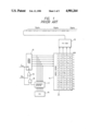
- FIG. 1 shows an example of the arrangement of a conventional pseudo random pattern generating device using a memory system which can be implemented through utilization of relatively simple high speed technology alone.
- the 15-bit long basic random pattern "100110101111000” is split into 4-bit patterns, beginning with the leftmost four bits, and these split patterns are stored in the pattern memory 11.
- At address 0 is stored a 4-bit split pattern "1001”, at address 1 a 4-bit split pattern "1010”, at address 2 a 4-bit split pattern "1111”, and at address 3 a 4-bit split pattern "0001” which is a combination of the rightmost three bits "000” of the 15-bit basic random pattern and the leftmost bit "1" of the same basic random pattern "100110101111000” of second occurrence.
- a split pattern stored at the decoded address of the pattern memory 11 is read out therefrom and provided, as 4-bit parallel data, to a parallel-serial converter 15.
- the parallel-serial converter 15 converts the 4-bit split pattern into serial data and outputs it as a pseudo random pattern on a bitwise basis.
- the split patterns "1001”, “1010”, “1111” and “0001” are read out of the pattern memory 11 in that order.
- the basic random pattern "100110101111000” of first occurrence and the leftmost bit “1" of the basic random pattern of the next occurrence are output.
- the split patterns "0011”, “0101”, ... stored at addresses 4 to 14 are read out in a sequential order, thus creating a pseudo random pattern which provides the basic random pattern "100110101111000” in a repeating cyclic order.
- a numerical value "14" is set, as a stop code indicating the last address of the pattern memory 11, in a register 16.
- the set value "14" and the count value of the address counter 12 are provided to a coincidence detector 17.
- the coincidence detector 17 yields a coincidence detection signal, by which an AND gate 18 is enabled.
- the clock C which occurs after the detection of coincidence, is provided via the AND gate 18 and an OR gate 19 to the address counter 12, clearing it to zero. Consequently, the readout of the split pattern "1000" from address 14 is followed by the split pattern readout operation which starts again at address 0.
- Such a large-capacity memory is usually formed by a MOS memory, and hence requires a read cycle time which is so long that the high-speed generation of the pseudo random pattern calls for increasing of the number of bits of each split pattern, that is, the number of bits of one word which is stored at each address.
- the number of bits of each split pattern is 256 bits
- the 2 n-m subpatterns thus obtained are stored in a pattern memory at 2 n-m addresses and read out therefrom in a repeating cyclic order.
- the pseudo random pattern generating device of the present invention is provided with a 2 n-m -counter as an address counter which counts clocks and provides addresses to the pattern memory for readout thereof, shift means whereby upon each completion of the readout of all the 2 n-m subpatterns from the pattern memory the 2 m -bit continuation pattern subsequent to each subpattern read out of the pattern memory is shifted one bit position and is output, a latch for latching the 2 m -bit continuation pattern output from the shift means, and a parallel-serial converter for converting the latched pattern into a serial pattern for output therefrom.
- a 2 n-m -counter as an address counter which counts clocks and provides addresses to the pattern memory for readout thereof
- shift means whereby upon each completion of the readout of all the 2 n-m subpatterns from the pattern memory the 2 m -bit continuation pattern subsequent to each subpattern read out of the pattern memory is shifted one bit position and is output
- a latch for latching the 2 m -
- FIG. 1 is a diagram showing an example of a conventional pseudo random pattern generating device
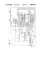
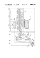
- FIG. 2 is a circuit diagram of the pseudo random pattern generating device according to the present invention.
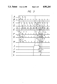
- FIG. 3 is a waveform diagram, for explaining the operation of the device shown in FIG. 2;
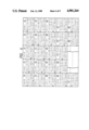
- FIG. 4 is a table showing how subpatterns stored in a pattern memory are sequentially rotated left.
- FIG. 5 is a circuit diagram illustrating another embodiment of the present invention.
- FIG. 2 is a circuit diagram illustrating an embodiment of the pseudo randompattern generating device of the present invention.
- a basic random pattern which recurs on a cycle of 2 n -1 bits is split every 2 m bits into 2 n-m split patterns.Each split pattern is combined with a continuation pattern composed of 2 m bits subsequent thereto in the recurring basic random pattern, obtaining 2 n-m subpatterns each of 2 m+ 1 bits in length.
- the 2 n-m subpatterns are prestored in a pattern memory.
- the pseudo random generating device of the present invention comprises a pattern generator 21 and its controller 22.
- the pattern generator 21 comprises the (8 bits ⁇ 4 words) pattern memory 23 for storing subpatterns, a 9-stage shift register 24 which is supplied with an 8-bit output from the pattern memory 23, a latch 25 whichis made up of four registers R 1 to R 4 and supplied with a portionof a parallel output from the shift register 24, a parallel-serial converter 26 which is supplied with the output from the latch 25, and two selectors 27 and 28, each composed of eight ganged switches, for interconnecting the input and output terminals of the pattern memory 23 and the shift register 24.
- Outputs D0 to D7 of first to eighth bits of the pattern memory 23 are connected to eight switches S 1 to S 8 of the readout selector 27 at one input contacts C 1 , the outputs of D4 to D7 of the fifth to eighth bits of the pattern memory 23 are connected to the other input contacts C 2 of the left-hand switches S 1 to S 4 of the selector 27, and the outputs D0 to D3 of the first to fourth bits of the pattern memory 23 are connected to the other input contacts C 2 of theright-hand switches S 5 to S 8 of the selector 27.
- the readout switches S 1 to S 8 are arranged so that they supply, second to ninth shift stages b to i of the shift register 24 with signals applied tothe input contacts C 1 or C 2 , under control of a select signal which is provided to a control terminal 29.
- the outputs of the first to fourth shift stages a to d of the shift register 24 are provided to the first to fourth registers R 1 to R 4 of the latch 25, the outputs of which are applied to the parallel-serial converter 26.
- the parallel-serial converter 26 converts the applied data into serial data and outputs it as a pseudo random pattern on a bitwise basis.
- the outputs of the second to ninth shift stages b to i of the shift register 24 are applied to first to eighth switches S 1 to S 8 of the write selector 28 at one input contacts C 1 thereof.
- the outputs of the sixth to ninth shift stages f to i of theshift register 24 are applied to the other input contacts C 2 of the first to fourth switches S 1 to S 4 of the write selector 28 and the outputs of the second to fifth shift stages b to e are applied to the other input contacts C 2 of the fifth to eighth switches S 5 to S 8 of the selector 28, respectively.
- These switches S 1 to S 8 are arranged so that the signals applied to the input contacts C 1 or C 2 are provided as data D0 to D7 for write into the first to eighth bits of the pattern memory 23, under control of a select signal which is applied to a control terminal 29.
- the output of the second shift stage b of the shift register 24 is provided to a serial data input terminal Sin of the ninth shift stage i.
- a start signal A and a clock B are applied to the controller 22, wherein various control signals are created for controlling the pattern generator 21.
- the clock B is provided to a trigger terminal T of a J-K flip-flop 33, AND gates 34 and 35 and an OR gate 36.
- the flip-flop 33 is supplied at its J and K terminals with high- and low-level signals, respectively, and provides a high-level signal at its Q output terminal in response to the fall of the signal applied to the trigger terminal T.
- the output signal C of the flip-flop 33 is applied as a gate control signal to one input terminal of each of AND gates 34, 35, 37 and 38.
- the control signal is a high-level signal and hence is an enable signal
- these AND gates 34, 35, 37 and 38 are enabled, from which control signals applied to the otherinput terminals are output from their output terminals. Accordingly, when the AND gate 34 is enabled, the clock B supplied to the other input terminal thereof is provided therethrough to a counter 41 via an OR gate 39.
- the counter 41 is a 2 n counter.
- the maximum count value of an address counter 42 is selected equal to the number of subpatterns into which the basic random pattern is split every 2 m bits.
- the low-order two digits of the 2 n counter 41 which is a 2 4 counter in this case, are shared with the address counter 42, and count outputs A1 and A2 of the low-order two digits are provided as address signals to an address decoder 44 in the pattern memory23.
- the output of the most significant digit A4 is applied to a pulse generator 45, whose output is provided to another pulse generator 46 and via the OR gate 39 to the counter 41.
- the output pulse of the pulse generator 46 and the clock B are both applied via the OR gate 36 to a delay circuit 47, wherein they are delayed by ⁇ 1 , and the delayedoutput is provided as a readout pulse F to the shift register 24 via the AND gate 37.
- This delayed output is provided to another delay circuit 48, wherein it is further delayed by ⁇ 2 , and this delayed output is applied as a left shift pulse G to the shift register 24 via the AND gate 38.
- the left shift pulse B is supplied as a write pulse H to the pattern memory 23 via a delay circuit 49.
- the output A4 of the 2 4 counter 41 is applied as a trigger signal I to a flip-flop 43.
- the flip-flop 43 is being supplied at its J and K terminalswith high-level signals and inverts the level of an output signal at its Q output terminal upon each application of the trigger signal.
- the output ofthe flip-flop 43 is provided to the control terminals of the selectors 27 and 28 as the afore-mentioned select signal J for selecting their contactsC 1 or C 2 .
- the four subpatterns are stored in the pattern memory 23 at addresses 0 to 3 in right order, as indicated by "0s" and "1s" in FIG. 2.
- an 8-bit subpattern "10011010” composed of the first eight bits of the basic random pattern "100110101111000"
- address 1 an 8-bit subpattern "10101111” composed ofthe 5th to 12th bits of the basic random pattern
- an 8-bit subpattern "11110001” composed of the 9th to 15th bits of the basic randompattern and the first bit of the next basic random pattern
- address 3 an 8-bit subpattern "00010011” composed of the 13th to 15th bits of the first basic random pattern and the first to 5th bits of the next basic random pattern.
- FIGS. 3A to 3L show a series of waveforms occurring at respective parts of the controller 22, for explaining the operation of reading out the subpatterns stored in the pattern memory 23 and generating a pseudo randompattern which repeats the same pattern periodically at intervals of 15 bits.
- the waveform A indicates the start signal A and the waveform B the clock B.
- FIG. 4 is a transition diagram showing how the stored contents ofthe subpatterns in the pattern memory 23 change in the course of control for the generation of the pseudo random pattern. Fields ⁇ 1 , ⁇ 2 ,..., ⁇ 16 , ⁇ 1 ', ⁇ 2 ', ...
- the fields ⁇ 1 , ⁇ 2 , ... in FIG. 4 each show the currently stored contents of subpatterns in the pattern memory 23 and a 4-bit pattern readout in the immediately preceding field and currently output from the latch 25.
- the field ⁇ 0 shows the initial state ofthe pattern memory 23, that is, the stored contents of subpatterns in the pattern memory 23 prior to the start of operation; namely, the subpatterns "10011010", “10101111”, “11110001” and "0010011” are stored at addresses 0, 1, 2 and 3, respectively.
- the vertical broken lines shown before the respective subpatterns indicate the positions of splitting the basic random pattern into 4-bit lengths.
- the pattern splitting positions are cyclically shifted left as control proceeds. For example, in the field ⁇ 1 showing the stored contents after one-clock control it is shownthat the subpattern at address 0 is cyclically shifted left one bit position, with the splitting position shifted between the seventh and eighth bits.
- the subpatterns at the subsequent addresses are also sequentially rotated left as shown in each field.
- the white trianglesshown at addresses 2 and 3 in the field ⁇ 0 indicate the ends of the 15-bit basic random pattern.
- the black triangle shown in each field indicates the address being currently specified.
- the 4-bit pattern shown at the high-order position in each field indicate a 4-bit pattern being currently latched in the latch 25.
- the flip-flops 33 and 43 and the counter 41 are released from the reset state and put into the ready state.
- the count values of the address counter 42 and the quaternary counter following it i.e. the high-order two digits ofthe 2 4 counter) are both zero.
- the signal C at the Q output terminal of the flip-flop 33 goes high in synchronism with the clock B 1 subsequent to the rise of the start signal A, and the high-level signal C is applied to the AND gates 34, 35, 37 and 38, enabling them.
- the counter 41 is a hexadecimal counter and the count output of its low-order two digits is utilized as the quaternary address counter 42.
- the clock B 1 cannot pass through the AND gate 34 because it has not been enabled yet at that instant, and the subsequent clocks B 2 , B 3 , ... pass through the AND gate 34 and are provided as sample clocks D 1 , D 2 , ... to the quaternary address counter 42.
- the sample clock C is counted by the address counter 42, whose quaternary count value is output as the address signal E (FIG. 3).
- the count output Eis applied to the address decoder 44 of the pattern memory 23, by the decoded output of which readout addresses of the pattern memory 23 are specified cyclically in the order of 0, 1, 2 and 3, as shown in row E of FIG. 3.
- the shift register 24 is formed by nine shift stages a to i and the output D0 to D7 of eight bits from the pattern memory 23 is provided via the selector 27 to the eight shift stages b to i.
- the clock B 1 supplied to the flip-flop 33 is delayed ⁇ 1 by the delay circuit 47, and consequently it is allowed to pass through the AND gate 37 already enabledat that time and is then applied as a read pulse F 1 to the shift register 24.
- the shift register 24 responds to the read pulse F 1 to read into the second to ninth shift stages b to i the 8-bit subpattern stored in the pattern memory 23 at address 0.
- the first shift stage a is not supplied with data and hence is undefined "X"; for example, when having read therein the subpattern stored at address 0, the shift register24 shows a pattern "X10011010".
- the clock B 1 delayed by the delay circuit 37 is further delayed ⁇ 2 by the delay circuit 48 and is then provided as a left shift pulse G (G 1 in row G of FIG. 3) to the shift register 24 via the AND gate 38.
- the left shift pulse G 1 the data "10011010" in the secondto ninth shift stages b to i is shifted one stage to the first to eighth shift stages a to h, respectively, and the data in the second shift stage b, "1" in this case, is supplied to the ninth shift stage i via the serialinput terminal Sin. Accordingly, the data in the shift register 24 changes to "100110101".
- the outputs of the second to ninth shift stages b to i of the shift register 24 are applied via the eight ganged write switches 28 to the pattern memory 23, wherein they are written again at the address from which they were read out, that is, at the address 0 in this instance. Thatis, the left shift pulse G 1 output from the AND gate 38 is delayed ⁇ 3 by a delay circuit 49, from which it is applied to a write pulse H 1 to the pattern memory 23, and the 8-bit output "00110101" from the second to ninth shift stages b to i of the shift register 24 is written at address 0. This means that the data "10011010" stored at address 0 before the write has been rotated left one bit position in its entirety (see the field ⁇ 1 in FIG. 4).
- the four outputs of the first to fourth shift stages a to d of theshift register 24 are latched by the sample clock D 1 (FIG. 3) in the 4-bit latch 25 composed of four registers R 1 to R 4 .
- data "1001" is latched in the latch 25, from which it is supplied to the parallel-serial converter 26.
- the left-hand 4-bit pattern "1001" of the 8-bit subpattern "10011010" stored at address 0 is provided to the parallel-serial converter 26 and atthe same time the 8-bit subpattern is rotated left one bit position and re-stored at address 0 (see the field ⁇ 1 in FIG. 4).
- the address counter 42 counts the sample clock D 1 (FIG. 3) and its count value goes to a "1" (row E).
- the subpattern "10101111” at address 1 is also read out similarly by a readout pulse F 2 and is rotated left by a shift pulse G 2 , thereafter being re-written into address 1 by a write pulse H 2 .
- the left-hand 4-bit pattern "1010" of the subpattern is latched in the latch 25 by a sample clock D 2 (see the field ⁇ 2 in FIG. 4).
- the left-hand 4-bit patterns "1111" and "0001" of the 8-bit subpatterns stored at addresses 2 and 3 are also latched in the latch 25, from which they are supplied to the parallel-serial converter 26.
- the subpatterns stored at addresses 2 and 3 are also rotatedleft one bit position and re-written into the addresses, respectively.
- the four subpatterns in the pattern memory 23 each have been rotated left one bit position (see the field ⁇ 4 in FIG. 4).
- the parallel-serial converter 26 converts each of the sequentially suppliedfour parallel 4-bit patterns "1001", “1010”, “1111” and "0001” into serial form, providing them as a serial data string "1001101011110001".
- the outputs of the left-hand first to fourth bits are selected fromthe outputs read out of addresses 0 to 3 on a cycle of four bits and are output in serial form, by which is generated the 16-bit pattern starting at the leftmost end of the subpattern "100110101" stored at address 0, that is, the pattern composed of the basic random pattern "100110101111000” and the "1" bit subsequent thereto.
- One cycle ends with a fourth clock D 4 by which the subpattern stored at address 3 is read out, and the count value of the address counter returns to zero (row F in FIG. 3).
- this state there are stored at the respective addresses of the pattern memory 23 8-bit subpatterns "00110101", “01011111”, “11100011” and "00100110” rotated left one bit position and hence starting at 2nd, 6th, 10th and 14th bits of the basic random pattern, respectively (see the field 4 in FIG. 4).
- the subpatterns stored in the pattern memory 23 are further rotated left one bit position (see the fields ⁇ 5 , ⁇ 6 , ⁇ 7 and ⁇ 8 in FIG. 4), with the result that there is stored at address 0 a subpattern "01101010". Accordingly, in the next 4-clock cycle a 16-bit pattern "0110101111000100” which starts at thethird bit of the basic random pattern "100110101111000” is created. In the 12-clock cycle so far, a total of three basic random patterns and a pattern "100" have been produced. The transition diagram of the pattern memory 23 in this case is shown in the field ⁇ 12 in FIG. 4.
- the status of the data stored in the pattern memory 23 is the same as the status in which the left- and right-hand 4-bit strings of the data shown in the field ⁇ 0 , which is the initial state, are exchanged with each other.
- the field ⁇ 16 et seq. even if each 8-bit subpattern is rotated left one bit position while reading out the left-hand four bits one after another in the same manner as in the fields ⁇ 0 to ⁇ 15 , the basic psedo random pattern cannot be correctly generated at and after a certain stage.
- the reason for this is that the fourth and fifth bits of each subpattern in the field ⁇ 16 become discontinuous in the recurring basic random pattern owing to such an exchange of the left- and right-hand data as mentioned above.
- the right-hand 4-bit pattern "1001" of the subpattern at address 0 in the field ⁇ 16 is the same as the pattern "1001" held in the latch 25 at thattime, the right-hand four bits of the subpattern read out of the address 0 in the field ⁇ 16 are not provided to the latch 25, but instead the subpattern is circularly shifted one bit position and the above-noted four bits are immediately re-written into address 0 of the pattern memory 23, and then the right-hand four bits of the subpattern at the next address are read out.
- the device of the present invention has such an arrangement as follows:
- the clock B is applied to the 2 n counter, that is, the 2 4 counter 41, and when 16 clocks B have been counted, the select signal J which is the Q output of the flip-flop 43 is inverted by the rise of the most significant digit A4 of the 2 4 counter 41. Bythis inversion the selectors 27 and 28 are switched to the input terminals C 2 .
- the outputs D4 to D7 of the fifth to eighth bits of the pattern memory 23 are provided to the second to fifth shift stages b to e of the shift register 24 via the first to fourth switches S 1 to S 4 of the selector 27, and the outputs D0 to D3 of the first to fourth bits are provided via the fifth to eighth switches S 5 to S 8 to the sixth to ninth shift stages f to i via the fifth to eighth switches S 5 to S 8 of the selector 27.
- the outputs of the sixth to ninth shift stages f to i are provided to the input terminals of the first to fourth bits of the pattern memory 23 via the first to fourth switches S 1 to S 4 of the selector 28, and the outputs of the second to fifth shift stages b to e are provided to the input terminals of the fifth to eighth bits of the pattern memory 23 via the fifth to eighth switches S 5 to S 8 of the selector 28.
- the select signal J is inverted and the outputs D0 to D3 and D4 to D7 of the pattern memory 23 are provided to the shift stages b to e and f to i of the shift register 24, respectively.
- the selectors 27 and 28 are switched between the input contacts C 1 and C 2 alternately with each other; accordingly those left- and right-hand four bits of the subpattern read out of the pattern memory 23 which are to be provided to the latch 25 are selected alternately with each other.
- the output I of the 2 n counter 41 is applied to the pulse generator 45.
- the pulse generator 45 responds to the fall of the output I of the 2 n counter 41 (row I in FIG. 3) to yield an adjust pulse K of a pulse width ⁇ 4 (row K).
- the adjust pulse K is applied via the OR gate 39 to the address counter 42, incrementing its count value by one (row E).
- the adjust pulse K is supplied to the pulse generator 46 as well and its output is applied as anadjust clock L via the OR gate 36, yielding a write pulse F' 2 (row F) and a left-shift pulse G' 2 (row G) of the shift register 24 and a re-write pulse H' 2 (row H) of the pattern memory 23.
- therespective control operations are performed corresponding to one clock, separately of the clock B.
- the pulse width ⁇ 4 of the adjust pulse K from the pulse generator 45 is selected larger than the sum of the delays ⁇ 1 , ⁇ 2 and ⁇ 3 . Therefore, even after completionof the write by the write pulse H' 1 the address counter 42 is incremented, by the trailing edge of the adjust pulse K of the pulse width ⁇ 4 , to "1" before the data of the second to fifth shift stages b to e of the shift register 24 is latched in the latch 25. Further, the pulse generator 46 is triggered by the trailing edge of the adjust pulse Kto yield the adjust clock L.
- the adjust clock L is provided, as the readoutpulse F' 2 for reading out the subpattern stored at address 1, the left-shift pulse G' 2 for shifting the read-out pattern to the left, and the write pulse H' 2 , to the shift register 24 and the pattern memory 23 via the delay circuits 47, 48 and 49.
- the subpattern stored at address 1 is rotated left one bit position and at thesame time its right-hand 4-bit pattern "1010" is latched by a sample clock D' 2 in the latch 25, from which it is supplied to the parallel-serialconverter 26.
- the readout, shift and re-write of the subpattern storedat address 0 are performed by a sequence of control pulses F' 1 , G' 1 and H' 1 following the sample clock D 16 shown in row D of FIG. 3.
- the pattern "1001" stored at address 0 is not latched in the latch 25 but instead the same pattern "1001" read out of address 3 in the previous cycle (the field ⁇ 15 in FIG. 4) is held in the latch 25.
- the pattern held in the latch 25 is shown as (1001) in the field ⁇ 1 ' in FIG. 4. This prevents the same pattern "1001"from being output from the latch 25 continuously for two clock cycles.
- the right-hand four bits "1010" of the subpattern are read out of address 2 and latched in the latch 25, thereafter being provided to the parallel-serial converter 26.
- a sequence of basic random patterns are cyclically generated until the field ⁇ 16 ' is reached.
- the adjust pulse K is produced again and the process returns to the field ⁇ 1 , after which the same operation as described above is repeated.
- This embodiment employs, as the pattern memory 23, a 2 n-m -word memoryin which one word is (2 m+1 -1) bits long.
- a (7 bits ⁇ 4 words) pattern memory is used in this embodiment.
- the data outputs D0 to D6 of seven bits of the pattern memory 23 are applied to a multiplexer 51, from which a 4-bit data output corresponding to select signals J 1 to J 4 which are selectively applied to select signal input terminal 32 is provided to the 4-bit latch circuit 25.
- the 4-bit pattern latched in the latch circuit 25 is provided to the parallel-serial converter 26, by which it is converted into serial data.
- the select signal J 1 is applied to a control terminal of each of gates1A, 1B, 1C and 1D, by which the outputs D0, D1, D2 and D3 of the first, second, third and fourth bits of the pattern memory 23 are applied to datainput terminals of the above-mentioned gates.
- the select signal J 2 is provided to a control terminal of each of gates 2A, 2B, 2C and 2D, by which the outputs D1, D2, D3 and D4 of the second, third, fourth and fifthbits of the pattern memory 23 are supplied to data input terminals of thesegates.
- the select signal J 3 is provided to a control terminal of each of gates 3A, 3B, 3C and 3D, by which the outputs D2, D3, D4 and D5 of the third, fourth, fifth and sixth bits of the pattern memory 23 are applied to data input terminals of these gates.
- the select signal J 4 is provided to a control terminal of each of gates 4A, 4B, 4C and 4D, by which the outputs D3, D4, D5 and D6 of the fourth, fifth, sixth and seventh bits of the pattern memory 23 are applied to data input terminals of these gates.
- the select signal J 1 when the select signal J 1 is applied to the multiplexer 51, the data outputs D0 to D3 of the first to fourth bits of the pattern memory 23 are provided to the latch 25; when the select signalJ 2 is applied to the multiplexer 51, the data outputs D1 to D4 of the second to fifth bits of the pattern memory 23 are provided to the latch 25; when the select signal J 3 is applied to the multiplexer 51, the data outputs D2 to D5 of the third to sixth bits of the pattern memory 23 are provided to the latch 25; and when the select signal J 4 is applied to the multiplexer 51, the data outputs D3 to D6 of the fourth to seventh bits of the pattern memory 23 are provided to the latch 25.
- the controller 22 is supplied with the start signal A and the clock B, and control of respective parts is effected in synchronism with the clock B.
- the start signal A is applied to reset terminals R of the flip-flop 33, a 2 n-m counter 42 1 and 2 m counter 42 2 , initializing them.
- the maximum count value of the 2 n-m counter is equal to the number 2 n-m of patterns into which the basic random pattern is split at intervals of 2 m bits, and the maximum count value of the 2 m counter 42 2 is equal to the bit length 2 m of each split pattern.
- the output of the flip-flop 33 is provided to one input terminal of the ANDgate 34, which is supplied at the other input terminal with the clock B. Insynchronism with the fall of the clock B, the Q output of the flip-flop 33 becomes a high-level signal.
- the AND gate 34 is enabled by this high-level signal, the clock B is applied therethrough to the latch 25 andthe 2 n-m counter 42 1 .
- the latch 25 loads thereinto the output of the pattern memory 23 through the multiplexer 51 in synchronism with the rise of the clock B.
- the 2 n-m counter 42 1 increments its count value in synchronism with the fall of the clock B applied to its clock terminal T and the count output is provided as an address signal to the address decoder 44 of the pattern memory 23.
- the address of the pattern memory 23 to be read out is specified. Accordingly, a 4-bit pattern is latched by the leading edge of the clock B into the latch 25 from the pattern memory 23 and the address is incremented by the trailing edge of the clock B in preparation for the next latching operation.
- a high-order digit output A2 of the 2 n-m counter 42 1 is provided as a count pulse to the 2 m counter 42 2 , the count value of whichis incremented by the fall of the pulse.
- the count outputs A3 and A4 of the2 m counter 42 2 are supplied to a selector 31, which supplies the select terminal 32 of the multiplexer 51 with that one of the select signals J 1 to J 4 which corresponds to the applied count value.
- the high-order digit output A4 of the 2 m counter 42 2 is supplied to the pulse generator 45, from which the adjust pulse K is provided to aninitialization terminal L of the 2 n-m counter 42 1 .
- the adjust pulse K is applied, the count value of the 2 n-m counter 42 1 is set to a "1".
- the basic random pattern "100110101111000” is split at intervals of four bits into 2 n-m patterns and each split pattern is combined with a continuation pattern composed of three bits subsequent thereto in the recurrence of thebasic random pattern, forming a 7-bit subpattern.
- the 7-bit subpatterns arestored in the pattern memory 23 whose word is 7-bits long.
- the Q output of the flip-flop 33 goes high in synchronism with the clock B which is applied first thereafter, and the AND gate 34 is enabled, through which the clock B is supplied to the 2 n-m counter 42 1 and the latch 25.
- the count value of the address counter 42 1 is incremented in synchronism with the fall of the clock B and the incremented count value is applied as an address signal to the decoder 44 of the pattern memory 23.
- theaddresses of the pattern memory 23 are specified cyclically in the order 0,1, 2, 3, 0, 1, 2, 3, ...
- the count value of the 2 m counter 42 2 is "0", on the basis of which the selector 31 applies the select signal J 1 to the select terminal 32 of the multiplexer 51
- the select signal J 1 the data outputs D0 to D3 of the first to fourth bits of the subpattern stored in the pattern memory 23 at address 0 are selected and supplied to the latch 25, wherein they can be latched in synchronism with the clock B.
- the latch 25 latches therein the 4-bit patterns "1001", “1010", “1111” and "0001" of the subpatterns stored at addresses 0 to 3 and provides them to the parallel-serial converter 26.
- the parallel-serialconverter 26 converts these four parallel 4-bit patterns in succession intoa sequence of serial data "1001101011110001". That is, one basic random pattern "10011010111100” and one bit "1" subsequent thereto are thus generated.
- the selector 31 After the operations corresponding to four clocks B the count value of the 2 m counter 42 2 goes up to "1". When supplied with this count value "1", the selector 31 provides the select signal J 2 to the multiplexer 51. Based on the select signal J 2 , the 4-bit patterns "0011”, “0101”, “1110” and “0010” of the second to fifth bits of the subpatterns stored at the respective addresses are read out of the patternmemory 23 by the next four clocks B from the 2 n-m counter 42 1 . The four 4-bit patterns thus read out of the pattern memory 23 are supplied to the parallel-serial converter 26, from which they are output as a sequence of serial data "0011010111100010". Thus two basic random patterns and a pattern "10” subsequent thereto have been generated in the previous and current 4-clock cycles.
- the count value of the 2 m counter 42 2 is incremented to "2".
- the count value "2" is applied to the selector 31, from which the select signal J 3 is provided to the multiplexer 51.
- the outputs D2 to D5 of the third to sixth bits of the respective subpatterns stored in the pattern memory 23 are read out and loaded into the latch 25.
- the four read-out outputs are then provided to the parallel-serial converter 26, from which is output a pattern "0110101111000100".
- the count value of the 2 m counter 42 2 is incremented to "3". Accordingly, the outputs of the fourth to seventh bits of the subpatterns stored in the pattern memory 23 at addresses 0 to 3 are sequentially read out and a 16-bit pattern "1101011110001001" is provided from the parallel-serial converter 26. Thus four basic random patterns anda pattern "1001" subsequent thereto have been generated so far.
- the count value of the 2 m counter 42 2 goes down to zero and the output A4 of its high-order digit falls, in synchronism with which the adjust pulse K is yielded from the pulse generator 45.
- the adjust pulse K the initial value "1" is set in the 2 n-m counter 42 1 .
- the first to fourth bit outputs of the subpattern "1010111” stored at address 1 are selected by the leading edge of the clock B and the pattern "1010” is latched. After this,the outputs of the first to fourth bits of the subpatterns stored at addresses 2 and 3 are similarly selected and latched. Accordingly, the patterns "1010", “1111” and "0001” are supplied to the parallel-serial converter 26, from which serial data "101011110001" is derived. That is, by combining the pattern "1001” generated in the previous cycle with the pattern "101011110001” in this cycle, the basic random pattern "100110101111000” and one bit “1” are obtained. Consequently, control for reading out a portion "1001" of the subpattern stored at address 0 is skipped over, making it possible to avoid an unnecessary repetition of thepattern readout operation.
- the count value of the 2 m counter 42 2 is made "1"
- the second to fifth bit outputs "0011", “0101", “1110” and "0010” of the subpatterns stored in the pattern memory 23 at the respective addresses thereof are sequentially read out, latched and applied to the parallel-serial converter 26, from which serial data "0011010111100010” isyielded.
- the third to sixth bit outputs are sequentially read out of address 0, latched and supplied to the parallel-serial converter 26, from which serial data "0110101111000100" isderived.
- the fourth to seventh bit outputs are sequentiallyread out of addresses 0 to 3, generating serial data "1101011110001001".
- the subpattern readout address is adjusted by the adjust pulse K which is produced by the pulse generator 45.
- the pattern memory for storing the basic random pattern is formed by a memory of a very smallcapacity and the control for generating the pseudo random pattern can be implemented by use of a simple high-speed readout control technique alone.
- the present invention is of particular utility when employed in the case where the high-speed generation of a pseudo random pattern is needed as in the field of digital communications.
Landscapes
- Engineering & Computer Science (AREA)
- General Physics & Mathematics (AREA)
- Theoretical Computer Science (AREA)
- Signal Processing (AREA)
- Physics & Mathematics (AREA)
- Computer Networks & Wireless Communication (AREA)
- Computer Security & Cryptography (AREA)
- Computational Mathematics (AREA)
- Mathematical Optimization (AREA)
- Pure & Applied Mathematics (AREA)
- General Engineering & Computer Science (AREA)
- Mathematical Analysis (AREA)
- Complex Calculations (AREA)
- Tests Of Electronic Circuits (AREA)
- Manipulation Of Pulses (AREA)
Applications Claiming Priority (4)
| Application Number | Priority Date | Filing Date | Title |
|---|---|---|---|
| JP62192157A JP2719681B2 (ja) | 1987-07-31 | 1987-07-31 | 擬似ランダムパターン発生器 |
| JP62192158A JPS6436213A (en) | 1987-07-31 | 1987-07-31 | Pseudo random pattern generator |
| JP62-192157 | 1987-07-31 | ||
| JP62-192158 | 1987-07-31 |
Publications (1)
| Publication Number | Publication Date |
|---|---|
| US4901264A true US4901264A (en) | 1990-02-13 |
Family
ID=26507144
Family Applications (1)
| Application Number | Title | Priority Date | Filing Date |
|---|---|---|---|
| US07/221,520 Expired - Fee Related US4901264A (en) | 1987-07-31 | 1988-07-20 | Pseudo random pattern generating device |
Country Status (3)
| Country | Link |
|---|---|
| US (1) | US4901264A (de) |
| EP (1) | EP0301383B1 (de) |
| DE (1) | DE3888421T2 (de) |
Cited By (14)
| Publication number | Priority date | Publication date | Assignee | Title |
|---|---|---|---|---|
| US5007016A (en) * | 1987-12-21 | 1991-04-09 | Compagnie Generale D'electricite | Fractal-type periodic temporal signal generator |
| US5251165A (en) * | 1992-04-09 | 1993-10-05 | James Iii J Colin | Two phase random number generator |
| AU699160B2 (en) * | 1994-12-26 | 1998-11-26 | Nec Corporation | Device and method for generating pseudorandom noise sequence |
| US6072823A (en) * | 1996-08-07 | 2000-06-06 | Matsushita Electric Industrial Co., Ltd. | Pseudo-random noise series generator |
| US6505226B1 (en) * | 1996-09-06 | 2003-01-07 | Hyundai Electronics Industries Co., Ltd. | High speed parallel adder |
| US20030101392A1 (en) * | 2001-11-26 | 2003-05-29 | Lee Chen-Tsai | Method of testing memory with continuous, varying data |
| US6625199B1 (en) | 1999-05-28 | 2003-09-23 | Texas Instruments Incorporated | Methods and apparatus for use in simultaneously generating multiple data sequences using a single data access module |
| US6748006B1 (en) | 1999-05-28 | 2004-06-08 | Texas Instruments Incorporated | Method and apparatus for controlling system timing with use of a master timer |
| KR100439284B1 (ko) * | 1995-02-01 | 2004-09-07 | 코닌클리케 필립스 일렉트로닉스 엔.브이. | 순열유닛을구비한회로장치및아이템군처리방법 |
| US20050190818A1 (en) * | 2002-10-11 | 2005-09-01 | Sumimasa Sunaga | PN code generator, GOLD code generator, PN code despreader, method for generating PN code, method for generating GOLD code, method for despreading PN code and computer program |
| US20090083361A1 (en) * | 2007-09-24 | 2009-03-26 | Moore Charles H | Shift-add based multiplication |
| US7516280B1 (en) * | 2004-03-30 | 2009-04-07 | Cypress Semiconductor Corporation | Pulsed arbitration system and method |
| US20130028041A1 (en) * | 2004-06-04 | 2013-01-31 | Paul Wilkinson Dent | Memory Compression |
| US20170299654A1 (en) * | 2016-04-19 | 2017-10-19 | International Business Machines Corporation | Implementing decreased scan data interdependence in on product multiple input signature register (opmisr) through prpg control rotation |
Families Citing this family (7)
| Publication number | Priority date | Publication date | Assignee | Title |
|---|---|---|---|---|
| DE4139630A1 (de) * | 1991-11-30 | 1993-06-03 | Sel Alcatel Ag | Schaltungsanordnung zum erzeugen von binaeren pseudo-zufallsfolgen |
| DE4202682A1 (de) * | 1992-01-31 | 1993-08-05 | Sel Alcatel Ag | Paralleler additiver scrambler und descrambler |
| US5844925A (en) * | 1996-07-17 | 1998-12-01 | Ericsson Inc. | Spiral scrambling |
| WO2000025203A1 (en) * | 1998-10-28 | 2000-05-04 | Datamark Technologies Pte Ltd. | Methods of digital steganography for multimedia data |
| DE19963962C1 (de) * | 1999-12-31 | 2001-03-22 | Bosch Gmbh Robert | Pseudozufallsgenerator und Rundfunksender und Rundfunkempfänger |
| US6937643B2 (en) * | 2002-04-30 | 2005-08-30 | Qualcomm Inc | ROM-based PN generation for wireless communication |
| DE102008009924B4 (de) * | 2008-02-15 | 2014-10-30 | Jürgen Altenbrunn | Verfahren zum Generieren von Frequenzen |
Citations (3)
| Publication number | Priority date | Publication date | Assignee | Title |
|---|---|---|---|---|
| US4667301A (en) * | 1983-06-13 | 1987-05-19 | Control Data Corporation | Generator for pseudo-random numbers |
| US4748576A (en) * | 1984-02-06 | 1988-05-31 | U.S. Philips Corporation | Pseudo-random binary sequence generators |
| US4774681A (en) * | 1985-03-11 | 1988-09-27 | Tektronix, Inc. | Method and apparatus for providing a histogram |
Family Cites Families (1)
| Publication number | Priority date | Publication date | Assignee | Title |
|---|---|---|---|---|
| DE3513551A1 (de) * | 1985-04-16 | 1986-10-16 | Wandel & Goltermann Gmbh & Co, 7412 Eningen | Digitaler wortgenerator zur automatischen erzeugung periodischer dauerzeichen aus n-bit-woertern aller wortgewichte und deren permutationen |
-
1988
- 1988-07-19 EP EP88111619A patent/EP0301383B1/de not_active Expired - Lifetime
- 1988-07-19 DE DE3888421T patent/DE3888421T2/de not_active Expired - Fee Related
- 1988-07-20 US US07/221,520 patent/US4901264A/en not_active Expired - Fee Related
Patent Citations (3)
| Publication number | Priority date | Publication date | Assignee | Title |
|---|---|---|---|---|
| US4667301A (en) * | 1983-06-13 | 1987-05-19 | Control Data Corporation | Generator for pseudo-random numbers |
| US4748576A (en) * | 1984-02-06 | 1988-05-31 | U.S. Philips Corporation | Pseudo-random binary sequence generators |
| US4774681A (en) * | 1985-03-11 | 1988-09-27 | Tektronix, Inc. | Method and apparatus for providing a histogram |
Cited By (23)
| Publication number | Priority date | Publication date | Assignee | Title |
|---|---|---|---|---|
| US5007016A (en) * | 1987-12-21 | 1991-04-09 | Compagnie Generale D'electricite | Fractal-type periodic temporal signal generator |
| US5251165A (en) * | 1992-04-09 | 1993-10-05 | James Iii J Colin | Two phase random number generator |
| AU699160B2 (en) * | 1994-12-26 | 1998-11-26 | Nec Corporation | Device and method for generating pseudorandom noise sequence |
| KR100439284B1 (ko) * | 1995-02-01 | 2004-09-07 | 코닌클리케 필립스 일렉트로닉스 엔.브이. | 순열유닛을구비한회로장치및아이템군처리방법 |
| US6072823A (en) * | 1996-08-07 | 2000-06-06 | Matsushita Electric Industrial Co., Ltd. | Pseudo-random noise series generator |
| CN1082751C (zh) * | 1996-08-07 | 2002-04-10 | 松下电器产业株式会社 | 伪随机噪声序列发生器 |
| US6505226B1 (en) * | 1996-09-06 | 2003-01-07 | Hyundai Electronics Industries Co., Ltd. | High speed parallel adder |
| US6650687B1 (en) * | 1999-05-28 | 2003-11-18 | Texas Instruments Incorporated | Methods and apparatus for use in simultaneously generating data sequences for spread spectrum communications |
| US6748006B1 (en) | 1999-05-28 | 2004-06-08 | Texas Instruments Incorporated | Method and apparatus for controlling system timing with use of a master timer |
| US6625199B1 (en) | 1999-05-28 | 2003-09-23 | Texas Instruments Incorporated | Methods and apparatus for use in simultaneously generating multiple data sequences using a single data access module |
| US20030101392A1 (en) * | 2001-11-26 | 2003-05-29 | Lee Chen-Tsai | Method of testing memory with continuous, varying data |
| US7073101B2 (en) * | 2001-11-26 | 2006-07-04 | Winbond Electronics Corp. | Method of testing memory with continuous, varying data |
| US20050190818A1 (en) * | 2002-10-11 | 2005-09-01 | Sumimasa Sunaga | PN code generator, GOLD code generator, PN code despreader, method for generating PN code, method for generating GOLD code, method for despreading PN code and computer program |
| US7411993B2 (en) | 2002-10-11 | 2008-08-12 | Fujitsu Limited | PN code generator, GOLD code generator, PN code despreader, method for generating PN code, method for generating GOLD code, method for despreading PN code and computer program |
| US7516280B1 (en) * | 2004-03-30 | 2009-04-07 | Cypress Semiconductor Corporation | Pulsed arbitration system and method |
| US20130028041A1 (en) * | 2004-06-04 | 2013-01-31 | Paul Wilkinson Dent | Memory Compression |
| US8478804B2 (en) * | 2004-06-04 | 2013-07-02 | Telefonaktiebolaget Lm Ericsson (Publ) | Memory compression |
| US20090083360A1 (en) * | 2007-09-24 | 2009-03-26 | Gibson Dana Elliot | Shift-add based parallel multiplication |
| WO2009042111A3 (en) * | 2007-09-24 | 2009-06-25 | Vns Portfolio Llc | Shift-add based random number generation |
| US7774399B2 (en) | 2007-09-24 | 2010-08-10 | Vns Portfolio Llc | Shift-add based parallel multiplication |
| US20090083361A1 (en) * | 2007-09-24 | 2009-03-26 | Moore Charles H | Shift-add based multiplication |
| US20170299654A1 (en) * | 2016-04-19 | 2017-10-19 | International Business Machines Corporation | Implementing decreased scan data interdependence in on product multiple input signature register (opmisr) through prpg control rotation |
| US9964591B2 (en) * | 2016-04-19 | 2018-05-08 | International Business Machines Corporation | Implementing decreased scan data interdependence in on product multiple input signature register (OPMISR) through PRPG control rotation |
Also Published As
| Publication number | Publication date |
|---|---|
| DE3888421D1 (de) | 1994-04-21 |
| DE3888421T2 (de) | 1994-08-04 |
| EP0301383A3 (en) | 1990-02-28 |
| EP0301383B1 (de) | 1994-03-16 |
| EP0301383A2 (de) | 1989-02-01 |
Similar Documents
| Publication | Publication Date | Title |
|---|---|---|
| US4901264A (en) | Pseudo random pattern generating device | |
| US4593393A (en) | Quasi parallel cyclic redundancy checker | |
| US5548775A (en) | System and method for adaptive active monitoring of high speed data streams using finite state machines | |
| US4095283A (en) | First in-first out memory array containing special bits for replacement addressing | |
| US5416749A (en) | Data retrieval from sequential-access memory device | |
| US4413350A (en) | Programmable clock rate generator | |
| WO1987001836A1 (en) | Random sequence generators | |
| JPH0146919B2 (de) | ||
| US4755969A (en) | Pseudo random sequence generation | |
| GB2236934A (en) | Maximum length shift register sequence generator circuit | |
| AU597554B2 (en) | Pseudo-noise sequence generator | |
| US5708688A (en) | High speed programmable burst address generation circuit | |
| EP4325499A1 (de) | Auffrischungsadressenerzeugungsschaltung | |
| US4845726A (en) | Maximum length linearly recurring sequence generator control device | |
| US3787669A (en) | Test pattern generator | |
| EP0054159A2 (de) | Programmierbarer Zeitsteuerungsimpulsgeber | |
| RU154062U1 (ru) | Устройство для перебора перестановок | |
| US4719592A (en) | Sequence generator | |
| WO2023231263A1 (zh) | 一种刷新地址产生电路 | |
| EP0718848A2 (de) | Halbleiterspeicheranordnung mit Signalbündelübertragung | |
| US5822270A (en) | Circuit for generating internal column address suitable for burst mode | |
| US6633966B1 (en) | FIFO memory having reduced scale | |
| JP2719681B2 (ja) | 擬似ランダムパターン発生器 | |
| US4538260A (en) | Electronic time switch | |
| KR200155054Y1 (ko) | 카운터 회로 |
Legal Events
| Date | Code | Title | Description |
|---|---|---|---|
| AS | Assignment |
Owner name: ADVANTEST CORPORATION, 32-1, ASAHI-CHO 1-CHOME, NE Free format text: ASSIGNMENT OF ASSIGNORS INTEREST.;ASSIGNOR:HAYASHI, MISHIO;REEL/FRAME:004936/0335 Effective date: 19880701 |
|
| CC | Certificate of correction | ||
| FEPP | Fee payment procedure |
Free format text: PAYOR NUMBER ASSIGNED (ORIGINAL EVENT CODE: ASPN); ENTITY STATUS OF PATENT OWNER: LARGE ENTITY |
|
| FPAY | Fee payment |
Year of fee payment: 4 |
|
| REMI | Maintenance fee reminder mailed | ||
| LAPS | Lapse for failure to pay maintenance fees | ||
| FP | Lapsed due to failure to pay maintenance fee |
Effective date: 19980218 |
|
| STCH | Information on status: patent discontinuation |
Free format text: PATENT EXPIRED DUE TO NONPAYMENT OF MAINTENANCE FEES UNDER 37 CFR 1.362 |