US4901283A - Dynamic random-access memory system with power-up and power-down refresh circuits - Google Patents
Dynamic random-access memory system with power-up and power-down refresh circuits Download PDFInfo
- Publication number
- US4901283A US4901283A US07/266,391 US26639188A US4901283A US 4901283 A US4901283 A US 4901283A US 26639188 A US26639188 A US 26639188A US 4901283 A US4901283 A US 4901283A
- Authority
- US
- United States
- Prior art keywords
- power
- refresh
- predetermined frequency
- memory
- circuit
- Prior art date
- Legal status (The legal status is an assumption and is not a legal conclusion. Google has not performed a legal analysis and makes no representation as to the accuracy of the status listed.)
- Expired - Lifetime
Links
Images
Classifications
-
- G—PHYSICS
- G11—INFORMATION STORAGE
- G11C—STATIC STORES
- G11C11/00—Digital stores characterised by the use of particular electric or magnetic storage elements; Storage elements therefor
- G11C11/21—Digital stores characterised by the use of particular electric or magnetic storage elements; Storage elements therefor using electric elements
- G11C11/34—Digital stores characterised by the use of particular electric or magnetic storage elements; Storage elements therefor using electric elements using semiconductor devices
- G11C11/40—Digital stores characterised by the use of particular electric or magnetic storage elements; Storage elements therefor using electric elements using semiconductor devices using transistors
- G11C11/401—Digital stores characterised by the use of particular electric or magnetic storage elements; Storage elements therefor using electric elements using semiconductor devices using transistors forming cells needing refreshing or charge regeneration, i.e. dynamic cells
- G11C11/406—Management or control of the refreshing or charge-regeneration cycles
Definitions
- This invention relates to dynamic random-access memories (DRAMS).
- the contents of the DRAM may be lost. This can be avoided by providing some form of battery back-up for the memory, so that refreshing can continue even when the system is powered down.
- a dynamic random-access memory having a first refresh circuit for producing memory refresh cycles during a power-up condition, a second refresh circuit for producing memory refresh cycles during a power-down condition and having a lower power requirement than the first refresh circuit, and means operative during transition from the power-down condition to the power-up condition for temporarily increasing the frequency of the refresh cycles by the second refresh circuit, thereby providing a period in which no refresh cycles are required, to allow time for the first refresh circuit to become operative.
- the frequency of the first refresh circuit is increased for a short period after the transition. This further ensures that each location of the memory is refreshed within the prescribed cycle time.
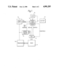
- FIG. 1 is a block diagram of a data processing system including a dynamic random-access memory (DRAM), with power-up and power-down refresh circuits.
- DRAM dynamic random-access memory
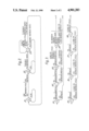
- FIGS. 2 and 3 are state diagrams describing the power-down refresh circuit.
- the system comprises a processor 10, connected to a DRAM 11 so that the processor can read and write data in a conventional manner.
- the DRAM 11 in this example holds 256K bytes, organised in 1024 rows and 256 columns.
- the DRAM has a memory control circuit 12, which may be of conventional form, for producing the normal row address strobe (RAS) and column address strobe (CAS) signals for the memory.
- RAS row address strobe
- CAS column address strobe
- the system also includes a power supply unit 13, for supplying power to theprocessor, DRAM, and memory control circuit.
- each refresh cycle consists of applying a CAS and then a RAS to the memory, i.e. reversing the normal order of RAS then CAS. This causes one selected column of the memory to be refreshed.
- the refresh cycle is performed for a different column every 15.625 microseconds, which means that the whole memory is refreshed every 4 milliseconds. This ensures thatthe memory contents are preserved.
- the control circuit 12 is conveniently implemented as a plurality of integrated-circuit gate arrays, and hence has a relatively high power requirement.
- the power-down refresh circuit comprises a single CMOS chip, and hence consumes only a relatively small amount of power.
- the power-down refresh circuit 14 receives a 512 KHz clock signal CLK from a clock circuit 16, which is also powered by the battery 15.
- the power supply 13 produces two control signals PS and DLYPS, to indicate its current state.
- PS is true (high) when the power supply is operating normally.
- the signal PS goes false (low) before the supply voltage falls out of specification.
- DLYPS follows PS after a delay of greater than 2 milliseconds.
- the control circuit 12 produces a control signal END PU REFRESH CYCLE to indicate the end of each power-up refresh cycle. This signal is fed to thepower-down refresh circuit 14.
- the system also includes a muliplexer 17, which normally selects the signals RAS and CAS from the memory control circuit 12 for application to the DRAM. When this multiplexer is switched, as will be described below, it selects alternative signals REFRAS and REFCAS from the power-down refresh circuit 14.
- the power-down refresh circuit 14 comprises two parts, referred to herein as the power-down/power-up control and the refresh control. Each of these parts is impemented in the form of a state machine, as defined by the state diagrams of FIGS. 2 and 3 respectively.
- the power-up/power-down control (FIG. 2) comprises three states 21-23, referred to hereinafter as states A-C.
- the refresh control (FIG. 3) comprises eight states 31-38, referred to hereinafter as states K-S.
- the power-down/power-up control (FIG. 2) communicates with the refresh control (FIG. 3) by means of the following signals:
- this signal also controls the multiplexer 17, so that when PD REFRESH is true, the signals REFRAS and REFCAS are routed to the DRAM in place of the normal RAS and CAS.
- the refresh control communicates with the power-down/power-up control by means of the following signal:
- each state is represented by a circle, and a transition between states is represented by an arrow.
- Each arrow is labelled with one or more conditions which must be satisfied before the transition can take place, followed (in brackets)by output signals that are effected by the transition.
- the arrow from state A to state B is labelled with the conditions END PU REFRESH CYCLE and /PS (where / denotes negation).
- END PU REFRESH CYCLE and /PS where / denotes negation.
- the signal PS goes true.
- the power-down/power-up control goes from state B to state C, and DOUBLE REFRESH RATE goes true.
- This signal causes the refresh control to loop back from state N to state K, so that it now cycles through the four states K-N, again producing a REFCAS and a REFRAS in each cycle.
- a refresh cycle is produced every 7.812 microseconds, so that the refresh rate is doubled.
- the signal DLYPS goes true. Then, at the first clock beat after END PD REFRESH CYCLE becomes true, the power-down/power-up control goes from state C to state A, and DOUBLE REFRESH RATE and PD REFRESH both become false. At the same time, the refresh control goes fromstate N to state K, and END PD REFRESH becomes false.
- PD REFRESH causes theprocessor 10 to come out of reset, and switches the multiplexer 17 (FIG. 1)so as to connect the normal control signals RAS and CAS to the memory.
- the state machines remain in states A and K respectively, until the next power-down.
- the memory control circuit 12 After the processor 10 has come out of reset the memory control circuit 12,under the control of software, doubles the refresh rate for a period of 2 milliseconds after which it reverts back to its normal rate. This ensures that those columns of memory refreshed at the beginning of the power-down refresh cycle are refreshed within 4 milliseconds of their last refresh.
- the refreshrate of the power-down refresh control 14 is doubled for 2 milliseconds before the processor comes out of reset. This builds up a surplus of refresh cycles, such that the DRAM does not have to be refreshed again foranother 2 milliseconds. This allows time for the processor to initialise the memory control circuit 12, so as to allow it to start performing refresh cycles again.
Landscapes
- Engineering & Computer Science (AREA)
- Microelectronics & Electronic Packaging (AREA)
- Computer Hardware Design (AREA)
- Dram (AREA)
Applications Claiming Priority (2)
| Application Number | Priority Date | Filing Date | Title |
|---|---|---|---|
| GB8801472 | 1988-01-22 | ||
| GB888801472A GB8801472D0 (en) | 1988-01-22 | 1988-01-22 | Dynamic random-access memory |
Publications (1)
| Publication Number | Publication Date |
|---|---|
| US4901283A true US4901283A (en) | 1990-02-13 |
Family
ID=10630396
Family Applications (1)
| Application Number | Title | Priority Date | Filing Date |
|---|---|---|---|
| US07/266,391 Expired - Lifetime US4901283A (en) | 1988-01-22 | 1988-11-02 | Dynamic random-access memory system with power-up and power-down refresh circuits |
Country Status (4)
| Country | Link |
|---|---|
| US (1) | US4901283A (fr) |
| EP (1) | EP0325026B1 (fr) |
| DE (1) | DE3876415T2 (fr) |
| GB (1) | GB8801472D0 (fr) |
Cited By (33)
| Publication number | Priority date | Publication date | Assignee | Title |
|---|---|---|---|---|
| WO1990016029A1 (fr) * | 1989-06-12 | 1990-12-27 | Grid Systems Corporation | Ordinateur de faible puissance a mode d'attente intermediaire |
| WO1992007317A1 (fr) * | 1990-10-12 | 1992-04-30 | Intel Corporation | Regeneration lente de la memoire d'un ordinateur fonctionnant avec une alimentation en puissance limitee |
| US5204840A (en) * | 1989-08-08 | 1993-04-20 | Mazur Jeffrey G | Means and methods for preserving microprocessor memory |
| US5229969A (en) * | 1991-04-15 | 1993-07-20 | Micron Technology, Inc. | Method for synchronizing refresh cycles in self-refreshing DRAMs having timing circuit shutdown |
| US5235691A (en) * | 1989-09-01 | 1993-08-10 | Oki Electric Industry Co., Ltd. | Main memory initializing system |
| US5274828A (en) * | 1992-02-24 | 1993-12-28 | Texas Instruments Incorporated | Computer including an integrated circuit having an on-chip high voltage source |
| DE4334415A1 (de) * | 1992-10-09 | 1994-04-14 | Mitsubishi Electric Corp | Dynamische Speichervorrichtung für wahlfreien Zugriff und Betriebsverfahren |
| WO1994012934A1 (fr) * | 1992-12-02 | 1994-06-09 | Performance Peripherals, Inc. | Regeneration alternee de memoire ram dynamique commandee par un detecteur de periode de signal |
| US5345574A (en) * | 1990-05-15 | 1994-09-06 | Seiko Epson Corporation | Memory card having controller providing adjustable refresh to a plurality of DRAMs |
| US5390333A (en) * | 1990-02-06 | 1995-02-14 | Alcatel Network Systems, Inc. | Switch array power reduction apparatus |
| US5392441A (en) * | 1989-01-27 | 1995-02-21 | Compaq Computer Corporation | Pump bus to avoid indeterminacy in reading variable bit field |
| US5392251A (en) * | 1993-07-13 | 1995-02-21 | Micron Semiconductor, Inc. | Controlling dynamic memory refresh cycle time |
| US5430881A (en) * | 1990-12-28 | 1995-07-04 | Dia Semicon Systems Incorporated | Supervisory control method and power saving control unit for computer system |
| US5438549A (en) * | 1994-02-28 | 1995-08-01 | Intel Corporation | Nonvolatile memory with volatile memory buffer and a backup power supply system |
| US5446696A (en) * | 1993-05-28 | 1995-08-29 | Rambus, Inc. | Method and apparatus for implementing refresh in a synchronous DRAM system |
| US5519831A (en) * | 1991-06-12 | 1996-05-21 | Intel Corporation | Non-volatile disk cache |
| US5548765A (en) * | 1990-08-28 | 1996-08-20 | Seiko Epson Corporation | Power saving display subsystem for portable computers |
| US5550781A (en) * | 1989-05-08 | 1996-08-27 | Hitachi Maxell, Ltd. | Semiconductor apparatus with two activating modes of different number of selected word lines at refreshing |
| US5555423A (en) * | 1991-11-19 | 1996-09-10 | Intel Corporation | Multi-mode microprocessor having a pin for resetting its register without purging its cache |
| US5633831A (en) * | 1994-02-03 | 1997-05-27 | Mitsubishi Denki Kabushiki Kaisha | Semiconductor memory device having self-refreshing function |
| US5712825A (en) * | 1996-10-09 | 1998-01-27 | International Business Machines Corporation | Maintaining data integrity in DRAM while varying operating voltages |
| US5781784A (en) * | 1992-07-09 | 1998-07-14 | Zilog, Inc. | Dynamic power management of solid state memories |
| US5859809A (en) * | 1996-12-31 | 1999-01-12 | Hyundai Electronics Industries Co., Ltd. | Semiconductor device of daisy chain structure having independent refresh apparatus |
| US6025737A (en) * | 1996-11-27 | 2000-02-15 | Altera Corporation | Circuitry for a low internal voltage integrated circuit |
| US6118302A (en) * | 1996-05-28 | 2000-09-12 | Altera Corporation | Interface for low-voltage semiconductor devices |
| US6134167A (en) * | 1998-06-04 | 2000-10-17 | Compaq Computer Corporation | Reducing power consumption in computer memory |
| US6175952B1 (en) | 1997-05-27 | 2001-01-16 | Altera Corporation | Technique of fabricating integrated circuits having interfaces compatible with different operating voltage conditions |
| US6201751B1 (en) * | 1999-03-08 | 2001-03-13 | Micron Technology, Inc. | Integrated circuit power-up controllers, integrated circuit power-up circuits, and integrated circuit power-up methods |
| US6243315B1 (en) | 1999-12-31 | 2001-06-05 | James B. Goodman | Computer memory system with a low power down mode |
| US6255850B1 (en) | 1997-10-28 | 2001-07-03 | Altera Corporation | Integrated circuit with both clamp protection and high impedance protection from input overshoot |
| KR100432700B1 (ko) * | 1998-10-06 | 2004-05-24 | 인텔 코오퍼레이션 | 저전력 상태로부터 dram 을 출구하기 위한자기-동기화 방법 및 장치 |
| US20060198225A1 (en) * | 2005-03-04 | 2006-09-07 | Seagate Technology Llc | Reducing power consumption in a data storage system |
| US20060291587A1 (en) * | 1997-06-20 | 2006-12-28 | Massachusetts Institute Of Technology | Digital transmitter |
Families Citing this family (4)
| Publication number | Priority date | Publication date | Assignee | Title |
|---|---|---|---|---|
| JPH04109488A (ja) * | 1990-08-29 | 1992-04-10 | Mitsubishi Electric Corp | ダイナミック型半導体記憶装置 |
| DE69128061T2 (de) * | 1990-08-30 | 1998-03-26 | Nippon Electric Co | Halbleiterspeicheranordnung |
| KR100413761B1 (ko) * | 2001-05-31 | 2003-12-31 | 삼성전자주식회사 | 온도와 공정에 따라 리프레시 사이클이 조절되는 반도체메모리 장치 및 방법 |
| EP1953619B1 (fr) * | 2007-02-01 | 2015-04-01 | Siemens Aktiengesellschaft | Procédé destiné à la sécurisation de données d'une installation de traitement des données et installation de traitement des données |
Citations (8)
| Publication number | Priority date | Publication date | Assignee | Title |
|---|---|---|---|---|
| US4313180A (en) * | 1979-01-30 | 1982-01-26 | Sharp Kabushiki Kaisha | Refresh system for a dynamic memory |
| US4316248A (en) * | 1978-12-06 | 1982-02-16 | Data General Corporation | Memory refresh means including means for providing refresh addresses during power failures |
| JPS60237522A (ja) * | 1984-05-10 | 1985-11-26 | Fujitsu Ltd | 論理回路装置 |
| US4616346A (en) * | 1983-03-04 | 1986-10-07 | Nec Corporation | Random access memory capable of varying a frequency in active and standby modes |
| US4625296A (en) * | 1984-01-17 | 1986-11-25 | The Perkin-Elmer Corporation | Memory refresh circuit with varying system transparency |
| US4631701A (en) * | 1983-10-31 | 1986-12-23 | Ncr Corporation | Dynamic random access memory refresh control system |
| US4701843A (en) * | 1985-04-01 | 1987-10-20 | Ncr Corporation | Refresh system for a page addressable memory |
| US4754425A (en) * | 1985-10-18 | 1988-06-28 | Gte Communication Systems Corporation | Dynamic random access memory refresh circuit selectively adapted to different clock frequencies |
Family Cites Families (1)
| Publication number | Priority date | Publication date | Assignee | Title |
|---|---|---|---|---|
| JPS59227090A (ja) * | 1983-06-06 | 1984-12-20 | Hitachi Ltd | 不揮発性メモリ装置 |
-
1988
- 1988-01-22 GB GB888801472A patent/GB8801472D0/en active Pending
- 1988-10-28 DE DE8888310148T patent/DE3876415T2/de not_active Expired - Fee Related
- 1988-10-28 EP EP88310148A patent/EP0325026B1/fr not_active Expired
- 1988-11-02 US US07/266,391 patent/US4901283A/en not_active Expired - Lifetime
Patent Citations (8)
| Publication number | Priority date | Publication date | Assignee | Title |
|---|---|---|---|---|
| US4316248A (en) * | 1978-12-06 | 1982-02-16 | Data General Corporation | Memory refresh means including means for providing refresh addresses during power failures |
| US4313180A (en) * | 1979-01-30 | 1982-01-26 | Sharp Kabushiki Kaisha | Refresh system for a dynamic memory |
| US4616346A (en) * | 1983-03-04 | 1986-10-07 | Nec Corporation | Random access memory capable of varying a frequency in active and standby modes |
| US4631701A (en) * | 1983-10-31 | 1986-12-23 | Ncr Corporation | Dynamic random access memory refresh control system |
| US4625296A (en) * | 1984-01-17 | 1986-11-25 | The Perkin-Elmer Corporation | Memory refresh circuit with varying system transparency |
| JPS60237522A (ja) * | 1984-05-10 | 1985-11-26 | Fujitsu Ltd | 論理回路装置 |
| US4701843A (en) * | 1985-04-01 | 1987-10-20 | Ncr Corporation | Refresh system for a page addressable memory |
| US4754425A (en) * | 1985-10-18 | 1988-06-28 | Gte Communication Systems Corporation | Dynamic random access memory refresh circuit selectively adapted to different clock frequencies |
Cited By (67)
| Publication number | Priority date | Publication date | Assignee | Title |
|---|---|---|---|---|
| US5392441A (en) * | 1989-01-27 | 1995-02-21 | Compaq Computer Corporation | Pump bus to avoid indeterminacy in reading variable bit field |
| US5550781A (en) * | 1989-05-08 | 1996-08-27 | Hitachi Maxell, Ltd. | Semiconductor apparatus with two activating modes of different number of selected word lines at refreshing |
| WO1990016029A1 (fr) * | 1989-06-12 | 1990-12-27 | Grid Systems Corporation | Ordinateur de faible puissance a mode d'attente intermediaire |
| US5204840A (en) * | 1989-08-08 | 1993-04-20 | Mazur Jeffrey G | Means and methods for preserving microprocessor memory |
| US5235691A (en) * | 1989-09-01 | 1993-08-10 | Oki Electric Industry Co., Ltd. | Main memory initializing system |
| US5390333A (en) * | 1990-02-06 | 1995-02-14 | Alcatel Network Systems, Inc. | Switch array power reduction apparatus |
| US5345574A (en) * | 1990-05-15 | 1994-09-06 | Seiko Epson Corporation | Memory card having controller providing adjustable refresh to a plurality of DRAMs |
| US5548765A (en) * | 1990-08-28 | 1996-08-20 | Seiko Epson Corporation | Power saving display subsystem for portable computers |
| GB2264799A (en) * | 1990-10-12 | 1993-09-08 | Intel Corp | Slow memory refresh in a computer with a limited supply of power |
| WO1992007317A1 (fr) * | 1990-10-12 | 1992-04-30 | Intel Corporation | Regeneration lente de la memoire d'un ordinateur fonctionnant avec une alimentation en puissance limitee |
| GB2264799B (en) * | 1990-10-12 | 1994-11-16 | Intel Corp | Slow memory refresh in a computer with a limited supply of power |
| US5465367A (en) * | 1990-10-12 | 1995-11-07 | Intel Corporation | Slow memory refresh in a computer with a limited supply of power |
| US5430881A (en) * | 1990-12-28 | 1995-07-04 | Dia Semicon Systems Incorporated | Supervisory control method and power saving control unit for computer system |
| US5229969A (en) * | 1991-04-15 | 1993-07-20 | Micron Technology, Inc. | Method for synchronizing refresh cycles in self-refreshing DRAMs having timing circuit shutdown |
| US5519831A (en) * | 1991-06-12 | 1996-05-21 | Intel Corporation | Non-volatile disk cache |
| US5555423A (en) * | 1991-11-19 | 1996-09-10 | Intel Corporation | Multi-mode microprocessor having a pin for resetting its register without purging its cache |
| US5274828A (en) * | 1992-02-24 | 1993-12-28 | Texas Instruments Incorporated | Computer including an integrated circuit having an on-chip high voltage source |
| US5781784A (en) * | 1992-07-09 | 1998-07-14 | Zilog, Inc. | Dynamic power management of solid state memories |
| DE4334415A1 (de) * | 1992-10-09 | 1994-04-14 | Mitsubishi Electric Corp | Dynamische Speichervorrichtung für wahlfreien Zugriff und Betriebsverfahren |
| US5321662A (en) * | 1992-10-09 | 1994-06-14 | Mitsubishi Denki Kabushiki Kaisha | Dynamic random access memory device having a self refresh mode |
| US5421005A (en) * | 1992-12-02 | 1995-05-30 | Fiset; Peter D. | Alternate DRAM refresh controlled by signal period detector |
| WO1994012934A1 (fr) * | 1992-12-02 | 1994-06-09 | Performance Peripherals, Inc. | Regeneration alternee de memoire ram dynamique commandee par un detecteur de periode de signal |
| US5446696A (en) * | 1993-05-28 | 1995-08-29 | Rambus, Inc. | Method and apparatus for implementing refresh in a synchronous DRAM system |
| US5392251A (en) * | 1993-07-13 | 1995-02-21 | Micron Semiconductor, Inc. | Controlling dynamic memory refresh cycle time |
| US5539703A (en) * | 1993-07-13 | 1996-07-23 | Micron Technology, Inc. | Dynamic memory device including apparatus for controlling refresh cycle time |
| US5633831A (en) * | 1994-02-03 | 1997-05-27 | Mitsubishi Denki Kabushiki Kaisha | Semiconductor memory device having self-refreshing function |
| US5825705A (en) * | 1994-02-03 | 1998-10-20 | Mitsubishi Denki Kabushiki Kaisha | Semiconductor memory device having self-refreshing function |
| US5438549A (en) * | 1994-02-28 | 1995-08-01 | Intel Corporation | Nonvolatile memory with volatile memory buffer and a backup power supply system |
| US6147511A (en) * | 1996-05-28 | 2000-11-14 | Altera Corporation | Overvoltage-tolerant interface for integrated circuits |
| US6604228B1 (en) * | 1996-05-28 | 2003-08-05 | Altera Corporation | Technique of fabricating integrated circuits having interfaces compatible with different operating voltage conditions |
| US6433585B1 (en) | 1996-05-28 | 2002-08-13 | Altera Corporation | Overvoltage-tolerant interface for integrated circuits |
| US6118302A (en) * | 1996-05-28 | 2000-09-12 | Altera Corporation | Interface for low-voltage semiconductor devices |
| US6724222B2 (en) | 1996-05-28 | 2004-04-20 | Altera Corporation | Programmable logic with lower internal voltage circuitry |
| US6344758B1 (en) | 1996-05-28 | 2002-02-05 | Altera Corporation | Interface for low-voltage semiconductor devices |
| US6342794B1 (en) | 1996-05-28 | 2002-01-29 | Altera Corporation | Interface for low-voltage semiconductor devices |
| US6563343B1 (en) | 1996-05-28 | 2003-05-13 | Altera Corporation | Circuitry for a low internal voltage |
| US6583646B1 (en) | 1996-05-28 | 2003-06-24 | Altera Corporation | Overvoltage-tolerant interface for integrated circuits |
| US6252422B1 (en) | 1996-05-28 | 2001-06-26 | Altera Corporation | Overvoltage-tolerant interface for intergrated circuits |
| US5712825A (en) * | 1996-10-09 | 1998-01-27 | International Business Machines Corporation | Maintaining data integrity in DRAM while varying operating voltages |
| US6025737A (en) * | 1996-11-27 | 2000-02-15 | Altera Corporation | Circuitry for a low internal voltage integrated circuit |
| US5859809A (en) * | 1996-12-31 | 1999-01-12 | Hyundai Electronics Industries Co., Ltd. | Semiconductor device of daisy chain structure having independent refresh apparatus |
| US6175952B1 (en) | 1997-05-27 | 2001-01-16 | Altera Corporation | Technique of fabricating integrated circuits having interfaces compatible with different operating voltage conditions |
| US8989303B2 (en) | 1997-06-20 | 2015-03-24 | Massachusetts Institute Of Technology | Digital transmitter |
| US20100034252A1 (en) * | 1997-06-20 | 2010-02-11 | Dally William J | Digital Transmitter |
| US9419824B2 (en) | 1997-06-20 | 2016-08-16 | Massachusetts Institute Of Technology | Digital transmitter |
| US9647857B2 (en) | 1997-06-20 | 2017-05-09 | Massachusetts Institute Of Technology | Digital transmitter |
| US8923433B2 (en) | 1997-06-20 | 2014-12-30 | Massachusetts Institute Of Technology | Digital transmitter |
| US8761235B2 (en) | 1997-06-20 | 2014-06-24 | Massachusetts Institute Of Technology | Digital transmitter |
| US20060291587A1 (en) * | 1997-06-20 | 2006-12-28 | Massachusetts Institute Of Technology | Digital transmitter |
| US8681837B2 (en) | 1997-06-20 | 2014-03-25 | Massachusetts Institute Of Technology | Digital Transmitter |
| US20090262794A1 (en) * | 1997-06-20 | 2009-10-22 | Massachusetts Institute Of Technology | Digital transmitter |
| US8311147B2 (en) | 1997-06-20 | 2012-11-13 | Massachusetts Institute Of Technology | Digital transmitter |
| US20110051794A1 (en) * | 1997-06-20 | 2011-03-03 | Massachusetts Institute Of Technology | Digital Transmitter |
| US20110135032A1 (en) * | 1997-06-20 | 2011-06-09 | Massachusetts Institute Of Technology | Digital transmitter |
| US20110200085A1 (en) * | 1997-06-20 | 2011-08-18 | Massachusetts Institute Of Technology | Digital Transmitter |
| US8238467B2 (en) | 1997-06-20 | 2012-08-07 | Massachusetts Institute Of Technology | Digital transmitter |
| US8238470B2 (en) | 1997-06-20 | 2012-08-07 | Massachusetts Institute Of Technology | Digital transmitter |
| US8243847B2 (en) | 1997-06-20 | 2012-08-14 | Massachusetts Institute Of Technology | Digital transmitter |
| US8254491B2 (en) | 1997-06-20 | 2012-08-28 | Massachusetts Institute Of Technology | Digital transmitter |
| US8259841B2 (en) | 1997-06-20 | 2012-09-04 | Massachusetts Institute Of Technology | Digital transmitter |
| US6255850B1 (en) | 1997-10-28 | 2001-07-03 | Altera Corporation | Integrated circuit with both clamp protection and high impedance protection from input overshoot |
| US6134167A (en) * | 1998-06-04 | 2000-10-17 | Compaq Computer Corporation | Reducing power consumption in computer memory |
| KR100432700B1 (ko) * | 1998-10-06 | 2004-05-24 | 인텔 코오퍼레이션 | 저전력 상태로부터 dram 을 출구하기 위한자기-동기화 방법 및 장치 |
| US6201751B1 (en) * | 1999-03-08 | 2001-03-13 | Micron Technology, Inc. | Integrated circuit power-up controllers, integrated circuit power-up circuits, and integrated circuit power-up methods |
| US6243315B1 (en) | 1999-12-31 | 2001-06-05 | James B. Goodman | Computer memory system with a low power down mode |
| US7177222B2 (en) * | 2005-03-04 | 2007-02-13 | Seagate Technology Llc | Reducing power consumption in a data storage system |
| US20060198225A1 (en) * | 2005-03-04 | 2006-09-07 | Seagate Technology Llc | Reducing power consumption in a data storage system |
Also Published As
| Publication number | Publication date |
|---|---|
| EP0325026A2 (fr) | 1989-07-26 |
| EP0325026B1 (fr) | 1992-12-02 |
| EP0325026A3 (en) | 1990-05-09 |
| GB8801472D0 (en) | 1988-02-24 |
| DE3876415T2 (de) | 1993-06-09 |
| DE3876415D1 (de) | 1993-01-14 |
Similar Documents
| Publication | Publication Date | Title |
|---|---|---|
| US4901283A (en) | Dynamic random-access memory system with power-up and power-down refresh circuits | |
| KR100381966B1 (ko) | 반도체메모리장치및그구동방법 | |
| US5262998A (en) | Dynamic random access memory with operational sleep mode | |
| EP0739015B1 (fr) | Dispositif de mémoire à semi-conducteurs | |
| KR100266118B1 (ko) | 반도체 기억장치 | |
| US7349277B2 (en) | Method and system for reducing the peak current in refreshing dynamic random access memory devices | |
| US6005818A (en) | Dynamic random access memory device with a latching mechanism that permits hidden refresh operations | |
| US5941990A (en) | Semiconductor integrated circuit having voltage generation circuit driven by two different clock signals | |
| US5335201A (en) | Method for providing synchronous refresh cycles in self-refreshing interruptable DRAMs | |
| JP4036536B2 (ja) | セルフ−リフレッシュモードを備えたdram装置 | |
| KR19990078379A (ko) | 디코딩 오토리프레시 모드를 가지는 디램 | |
| EP0647945A2 (fr) | Mode de raffraîchissement à rafale pour DRAMs | |
| US20040027900A1 (en) | Semiconductor memory device and system outputting refresh flag | |
| KR19990028991A (ko) | 파이프라인 어드레스 메모리와, 그것을 이용한 장치및 방법 | |
| US7522466B2 (en) | DRAM power bus control | |
| US20110194358A1 (en) | Semiconductor memory device using internal high power supply voltage in self-refresh operation mode and related method of operation | |
| US20050213408A1 (en) | Ripple refresh circuit and method for sequentially refreshing a semiconductor memory system | |
| KR100363107B1 (ko) | 반도체메모리 장치 | |
| US5208779A (en) | Circuit for providing synchronous refresh cycles in self-refreshing interruptable DRAMs | |
| US4494222A (en) | Processor system using on-chip refresh address generator for dynamic memory | |
| US5295110A (en) | Semiconductor memory device incorporated with self-refresh circuit | |
| KR0160531B1 (ko) | 반도체 메모리 소자 및 상기 반도체 메모리 소자의 동작을 제어하는 방법 | |
| KR100360738B1 (ko) | 반도체 회로 시험 방법 | |
| JP2003030985A (ja) | 半導体記憶装置の電源制御回路 | |
| KR100295985B1 (ko) | 디램을리프레쉬하기위한방법및장치 |
Legal Events
| Date | Code | Title | Description |
|---|---|---|---|
| AS | Assignment |
Owner name: INTERNATIONAL COMPUTERS LIMITED, ICL HOUSE, PUTNEY Free format text: ASSIGNMENT OF ASSIGNORS INTEREST.;ASSIGNORS:HANBURY, JONATHAN M.;BURTON, KEITH;REEL/FRAME:004995/0379;SIGNING DATES FROM 19881021 TO 19881024 |
|
| STCF | Information on status: patent grant |
Free format text: PATENTED CASE |
|
| FPAY | Fee payment |
Year of fee payment: 4 |
|
| FEPP | Fee payment procedure |
Free format text: PAYOR NUMBER ASSIGNED (ORIGINAL EVENT CODE: ASPN); ENTITY STATUS OF PATENT OWNER: LARGE ENTITY |
|
| FPAY | Fee payment |
Year of fee payment: 8 |
|
| FPAY | Fee payment |
Year of fee payment: 12 |