US4924149A - Apparatus for controlling the charging of a main capacitor of a flash unit - Google Patents
Apparatus for controlling the charging of a main capacitor of a flash unit Download PDFInfo
- Publication number
- US4924149A US4924149A US07/137,329 US13732987A US4924149A US 4924149 A US4924149 A US 4924149A US 13732987 A US13732987 A US 13732987A US 4924149 A US4924149 A US 4924149A
- Authority
- US
- United States
- Prior art keywords
- main capacitor
- charging
- converter
- flash
- voltage
- Prior art date
- Legal status (The legal status is an assumption and is not a legal conclusion. Google has not performed a legal analysis and makes no representation as to the accuracy of the status listed.)
- Expired - Lifetime
Links
Images


Classifications
-
- H—ELECTRICITY
- H05—ELECTRIC TECHNIQUES NOT OTHERWISE PROVIDED FOR
- H05B—ELECTRIC HEATING; ELECTRIC LIGHT SOURCES NOT OTHERWISE PROVIDED FOR; CIRCUIT ARRANGEMENTS FOR ELECTRIC LIGHT SOURCES, IN GENERAL
- H05B41/00—Circuit arrangements or apparatus for igniting or operating discharge lamps
- H05B41/14—Circuit arrangements
- H05B41/30—Circuit arrangements in which the lamp is fed by pulses, e.g. flash lamp
- H05B41/32—Circuit arrangements in which the lamp is fed by pulses, e.g. flash lamp for single flash operation
- H05B41/325—Circuit arrangements in which the lamp is fed by pulses, e.g. flash lamp for single flash operation by measuring the incident light
-
- Y—GENERAL TAGGING OF NEW TECHNOLOGICAL DEVELOPMENTS; GENERAL TAGGING OF CROSS-SECTIONAL TECHNOLOGIES SPANNING OVER SEVERAL SECTIONS OF THE IPC; TECHNICAL SUBJECTS COVERED BY FORMER USPC CROSS-REFERENCE ART COLLECTIONS [XRACs] AND DIGESTS
- Y10—TECHNICAL SUBJECTS COVERED BY FORMER USPC
- Y10S—TECHNICAL SUBJECTS COVERED BY FORMER USPC CROSS-REFERENCE ART COLLECTIONS [XRACs] AND DIGESTS
- Y10S315/00—Electric lamp and discharge devices: systems
- Y10S315/04—Dimming circuit for fluorescent lamps
-
- Y—GENERAL TAGGING OF NEW TECHNOLOGICAL DEVELOPMENTS; GENERAL TAGGING OF CROSS-SECTIONAL TECHNOLOGIES SPANNING OVER SEVERAL SECTIONS OF THE IPC; TECHNICAL SUBJECTS COVERED BY FORMER USPC CROSS-REFERENCE ART COLLECTIONS [XRACs] AND DIGESTS
- Y10—TECHNICAL SUBJECTS COVERED BY FORMER USPC
- Y10S—TECHNICAL SUBJECTS COVERED BY FORMER USPC CROSS-REFERENCE ART COLLECTIONS [XRACs] AND DIGESTS
- Y10S315/00—Electric lamp and discharge devices: systems
- Y10S315/05—Starting and operating circuit for fluorescent lamp
Definitions
- the present invention relates to a camera having a built-in flash which is provided with CPUs and, more particularly, to an apparatus for providing ON-OFF control over the charging of a main capacitor of a flash unit built in a photographic camera.
- a flash unit is disclosed, for example, in U.S. patent application No. 934,055 now U.S. Pat. No. 4,893,140.
- CPU one-chip microcomputers
- the time period taken until the level of the voltage V across the main capacitor reaches the level of a predetermined reference voltage V 2 is excessively extended and therefore the power consumption of a DC/DC converter and other circuits also increases. As a result, the number of flashes is reduced.
- an apparatus for controlling the charging of a main capacitor of a flash unit as shown in FIG. 1A which employs a single comparison means to detect the fact that the voltage V across a main capacitor C M has reached the reference voltage V 1 at which flash photographs can be taken, and then to employ a timer to detect the fact that a predetermined time period has elapsed after such detection so that the charging of the main capacitor C M is stopped.
- the comparison means is one in number and the CPU is provided with a timer function as a portion of the processing program executed by the CPU.
- an apparatus for controlling the charging of a main capacitor of a flash unit which is arranged, as shown in FIG. 1B, to employ comparison means to detect the fact that the level of the voltage V across the main capacitor C M has reached the level of the reference voltage V 1 and to perform recharging when the level of the voltage V drops to the level of the reference voltage V 1 as a result of the spontaneous discharge after completion of charging.
- an apparatus for controlling the charging of a main capacitor of a flash unit which is arranged, as shown in FIG. 1C, to permit flash photography if the time period required until the ensuing shutter release, after the voltage V across the main capacitor C M has reached the reference voltage V 2 (>V 1 ) at which flash photographs can be taken, is less than a predetermined value, and to inhibit flash photography to restart the charging of the main capacitor C M if the aforesaid time period is not less than the predetermined value. It is therefore possible to accomplish the advantages achieved in the first and second aspects of the invention. In this case, the reason why the number of flashes increases is that it is possible to prevent charging and discharging from being repeated many times.
- FIG. 1A is a block diagram illustrating the construction of a first aspect of the present invention
- FIG. 1B is a block diagram illustrating the construction of a second aspect of the present invention.
- FIG. 1C is a block diagram illustrating the construction of a third aspect of the preferred invention.
- FIG. 2 is a circuit diagram of the electronic flash circuit of a preferred embodiment of the invention in accordance with the first aspect thereof;
- FIG. 3 is a flow chart illustrating a process sequence of the steps executed by the CPU shown in FIG. 2;
- FIG. 4 is a flow chart illustrating a process sequence of the steps executed by a CPU in a preferred embodiment of the invention in accordance with the second aspect thereof;
- FIG. 5 is a circuit diagram of the electronic flash circuit of a second embodiment of the invention in accordance with the second aspect thereof;
- FIG. 6 is a flow chart illustrating a process sequence of the steps executed by the CPU shown in FIG. 5;
- FIG. 7 is a circuit diagram of the electronic flash circuit of a third embodiment of the invention in accordance with the second aspect thereof;
- FIG. 8 is a timing chart illustrating the voltage V across the main capacitor in comparison with variations in a flag F;
- FIG. 9 is a schematic illustration of a portion of the storage area of the RAM of the CPU shown in FIG. 2;
- FIG. 10 is a flow chart of a process sequence of the steps executed by a CPU in the invention in accordance with the third aspect thereof.
- FIG. 11 is a timing chart similar to FIG. 10, illustrating the voltage V developed across the main capacitor.
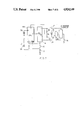
- FIG. 2 is a circuit diagram illustrating the electronic flash circuit incorporated in a photographic camera disclosed in U.S. patent application No. 934,055.
- the terminal voltage of a series of batteries 10 is applied to a DC/DC converter 14 through a flash switch 12 and, after being boosted, this applied voltage is stored as an electric charge in a main capacitor 16.
- An oscillation circuit which constitutes the DC/DC converter 14 is turned on and off by a control signal output from an output terminal C of a CPU 18, thereby providing control over the starting and stopping of the charging of the main capacitor 16.
- the CPU 18 is actuated by the direct application of the terminal voltage of the batteries 10.
- An input terminal A of the CPU 18 is connected to a battery voltage input terminal of the DC/DC converter 14.
- the CPU 18 is capable of detecting the opening and closing of the flash switch 12.
- Buses LP and LN are connected to the voltage output terminals of the DC/DC converter 14.
- a xenon discharge tube 20 and a trigger circuit 22 are connected in parallel between the buses LP and LN.
- a flash sync contact 24 is closed in a state wherein the level of the voltage V developed across the main capacitor 16 is equal to or higher than the level of the reference voltage V 1 , a high voltage is applied to a trigger electrode 26 to cause a discharge to take place, thereby causing the xenon discharge tube 20 to flash.
- a neon glow lamp 27 and a resistor 28 are connected in series between the buses LP and LN.
- V 1 the voltage developed across the main capacitor 16 reaches the aforesaid reference voltage V 1 .
- Voltage dividing resistors 30, 32 and 34 are connected in series between the bus LN and the junction of the neon glow lamp 27 and the resistor 28.
- the base of an NPN transistor 36 is connected to the junction of the voltage dividing resistors 32 and 34.
- the emitter of the NPN transistor 36 is connected to the bus LN while the collector is connected to the positive pole of the batteries 10 via the flash switch 12.
- the collector of the NPN transistor 36 is also connected to an input terminal B of the CPU 18.
- the NPN transistor 36 When the neon glow lamp 27 is OFF (V ⁇ V 1 ), the NPN transistor 36 is held in its OFF state and the potential at the input terminal B is held at a high level.
- the neon glow lamp 27 is turned on (V ⁇ V 1 )
- the NPN transistor 36 is turned on and the potential at the input terminal B goes to a low level. Accordingly, the CPU 18 can utilize such variations in the potential at the input terminal B to detect a point in time at which the level of the voltage V momentarily coincides with the level of the reference voltage V 1 .
- a zener diode 40 and a capacitor 42 are connected in parallel between the bus LN and the junction of the voltage dividing resistors 30 and 32.
- the zener diode 40 is provided for voltage clipping and the capacitor 42 is provided for noise elimination.
- the CPU 18 is a one-chip microcomputer provided with a timer function, and a timer interrupt takes place at predetermined intervals of, for example, 30 milliseconds.
- a timer interrupt takes place at predetermined intervals of, for example, 30 milliseconds.
- the values of timers T and T t which correspond to predetermined addresses of the RAM of the CPU 18 are incremented each time a timer interrupt occurs (the timer T t is used in an embodiment of the second aspect of the invention which will be described later).
- flags F 1 , F 2 and F 3 represent a time period during which the main capacitor 16 is being charged, and each of the flags F 1 , F 2 and F 3 varies, as shown in FIG. 9.
- FIG. 9 illustrates a preferred embodiment of the second aspect of the invention.
- the CPU 18 is adapted to write a state of charging C into a predetermined address of its RAM, and a main CPU (not shown) controls the entire circuit, causing an interrupt to occur in the CPU 18.
- Step 100 the process proceeds from Step 100 to Step 102, in which the value of the timer T is cleared and the flags F 1 and F 2 are reset. Then, in Step 103, the value representative of the state of charging C is reset to "0" (no charging), and the process returns to the routine which was executed immediately before this interrupt.
- Step 104 In which judgement is made as to whether or not the potential at the input terminal B has dropped to a predetermined level. Initially, the process proceeds to Steps 106 to 112 since a negative judgement is made in Step 104 because V ⁇ V 1 and because the flags F 1 and F 2 are reset in Step 102. In Step 112, it is normally judged that T ⁇ T 1 , and the process proceeds to Step 114. In Step 114, after the value of the state of charging C has been set to "1" (on charge), the process returns to the processing that was executed immediately before this interrupt.
- the time period T 1 is, for example, 30 seconds, and is allocated to allow the judgement to be made as to whether or not the battery is dead.
- Step 104 When the potential at the input terminal B rises to the predetermined level within the time period T 1 after the flash switch 12 has been turned on, the process proceeds from Step 104 to Step 116 in which the value of the timer T is cleared and flag F 1 is set to "1".
- Step 118 the process proceeds from Step 104 through Step 106 to Step 118 in which the value of the timer T is compared with the value of the time period T 2 .
- the value of the time period T 2 is, for example, 0.5 seconds and, if T ⁇ T 2 , the process returns to the processing that was executed immediately before this interrupt. If the level of the voltage V developed across the main capacitor 16 becomes V ⁇ V 1 as the result of the spontaneous discharge thereof, flash photography may become impossible within a short time between the moment at which the charging is stopped by turning on a release switch and the point at which the emission of flash light is started.
- the time period T 2 is used as a waiting time period allocated to allow prevention of occurrence of such a phenomenon.
- Step 124 the process proceeds from Step 104 through Steps 106 and 108 to Step 124 in which the value given by the timer T is compared with a time period T 3
- Steps 102A, 104A, and 128A are substituted for Steps 102, 104 and 128 illustrated in FIG. 3, and also Steps 110 and 130 to 136 are added.
- Step 102A a new flag F 3 is added, and in Step 102A the flag F 3 is reset.
- Step 104A when the potential at the input terminal B drops to the predetermined level and the flag F 3 is "0", the process proceeds to Step 116. If not, the process proceeds to Step 106.
- Step 128A the value of the timer T is cleared, the flag F 2 is reset, and the flag F 3 is set. Then, the process returns to the process which was executed immediately before this interrupt.
- Step 130 in which judgement is made as to whether the potential at the input terminal B has risen to the predetermined level. If a negative judgement is made in Step 130, the process returns to the processing that was executed immediately before this interrupt.
- Step 132 the value of the timer T is compared with the value of a time period T 4 .
- the time period T 4 is allocated to allow a judgement to be made as to whether or not the batteries are dead.
- Step 134 the CPU 18 supplies a control signal to the DC/DC converter 14 to activate the oscillation circuit and cause it to restart the charging of the main capacitor 16.
- Step 104A the process proceeds from Step 104A to Step 116 and subsequently the above-mentioned processing is repeated.
- this preferred embodiment provides the effect that enables a simple construction to be used to detect the dead state of the batteries even during the repetition of charging and discharging.
- the hardware arrangement of this embodiment is as shown in FIG. 5.
- a CPU 18A includes an A/D converter 18a and an LCD driver. Voltage dividing resistors 50 and 52 are connected in series between the buses LP and LN, and a potential V M (charging level) at the junction of the resistors 50 and 52 is supplied to an analog input terminal D of the A/D converter 18a.
- An LCD panel 54 is connected to an output terminal E of the LCD driver of the CPU 18A.
- the ON/OFF signal of a light metering switch (not shown) is input as an interrupt signal to an input terminal F of the CPU 18A, and the ON/OFF signal of a release switch 55 is input to an input terminal G of the CPU 18A.
- Steps 102B, 104B and 130B are substituted for Steps 102A, 104 and 130 shown in FIG. 4, and Steps 107 and 142 are added.
- a timer T t is newly incorporated and, in Step 102B, the timers T and T t are cleared. Accordingly, as shown in FIG. 9, the timer T t is started immediately after the start of charging.
- Step 104B judgement is made as to whether or not the charging level V M is higher than the level V 1 at which flash photography is enabled and as to whether or not the flag F 3 is "0".
- Step 107 inserted between Steps 106 and 108, a judgement is made as to whether T t >T 5 .
- T 5 is a value which is two to three times greater than, for example, T 4 , and is allocated to allow judgement to be made as to whether or not charging is automatically stopped in order to prevent the batteries from discharging when a photographer forgets to turn off the flash switch 12. If it is judged in Step 107 that T t ⁇ T 5 , the process proceeds to Step 108, in which the same processing as that described previously in connection with FIG. 4 is executed. If it is judged in Step 107 that T t ⁇ T 5 , Steps 138 and 140 are executed, and the timer interrupt is inhibited as described previously. When the light metering switch is turned on and the potential at the input terminal F of the CPU 18A reaches the high level, this inhibition is cancelled by an interrupt routine (not shown), thereby restarting the charging control.
- Step 130B it is judged from numerical values whether, as a result of the spontaneous discharge, the charging level V M has become lower than the potential V 1 at which flash photography is enabled.
- Step 142 indication bars equivalent in number to the charging level V M are displayed on the LCD panel 54 before the process returns to the processing which was executed immediately before this timer interrupt.
- indication bars illustrated in FIG. 5 short ones correspond to the state wherein charging has not yet been completed while long ones correspond to the state wherein charging has been completed. Accordingly, a photographer can check whether or not flash photography is possible; the extent of any insufficiency in charge; or the remaining capacity of the batteries in general terms with reference to the speed at which indication bars displayed increase in number.
- the hardware arrangement of this embodiment is as shown in FIG. 7.
- the anode of an LED 56 is connected to the positive pole of the batteries 10 and the cathode of the LED 56 is connected to an output terminal J of a CPU 18B.
- One terminal of a buzzer 58 employing a piezoelectric element is connected to an output terminal K of the CPU 18B, and the other terminal of the buzzer 58 is grounded.
- This CPU 18B includes a signal generator whose signal output can be switched on and off by the program stored in the CPU 18B, and such signal output is provided at the output terminal K.
- Step 142 the processing in Step 142 is modified as follows. More specifically, if the charging level V M is equal to or higher than the level of the reference voltage V 1 , the level of the voltage at the output terminal J goes to the low level and the LED 56 is turned on. The signal generator is turned on and the buzzer 58 emits alarm sounds. The alarm sounds and the emission of the LED 56 inform a photographer of flash readiness.
- the other portion of the software arrangement is the same as that shown in FIG. 6.
- the hardware arrangement of this embodiment may comprise that of any of the above-described embodiments, but, by way of example, the following description is made in conjunction with the hardware arrangement illustrated in FIG. 5.
- FIG. 10 The software arrangement of this embodiment is illustrated in FIG. 10.
- the level of the voltage V developed across the main capacitor reaches the level of the reference voltage V 2 (>V 1 )
- Step 206 the process returns to the processing which was executed immediately before this interrupt In Step 206, the level of charge is displayed as "zero".
- Step 204 the process proceeds from Step 204 to Step 212 in which, on the basis of the signal supplied from the main CPU (not shown), judgement is made as to whether or not the emission of the flash lamp is needed. If it is judged that the emission is not needed because of the sufficient intensity of ambient light, the process returns to the processing which was executed immediately before this interrut If it is judged that no emission is needed, the process proceeds to Step 214 in which the value of the timer T, that is, the value of time period which passes between the point at which charging is stopped and the point at which the release switch 55 is switched on is equal to or greater than the fixed value T 6 .
- Step 216 a signal indicative of the permission of flash photography is supplied to the main CPU (not shown). Thus, exposure and film winding are performed.
- the process proceeds to Step 218 in which judgement is made as to whether a flash lamp has been flashed, that is, whether the voltage V M illustrated in FIG. 5 has reached substantial zero. If the flash lamp has been flashed, the process proceeds to Step 220, in which the value of the timer T is set to T 6 , and then returns to Step 208, in which charging is restarted.
- Step 220 is provided for causing the process to proceed from Step 214 to Step 222 when the release switch 55 is turned on prior to the completion of charging. If flashing does not occur because of a failure of the flash lamp or the like, recharging is not needed. Accordingly, the process returns from Step 218 to the processing which was executed immediately before this interrupt. Subsequently, Steps 200 to 206 are executed.
- Step 214 If it is judged in the aforesaid Step 214 that T ⁇ T 6 , the process proceeds to Step 222 in which the LCD panel is caused to display flash unreadiness. Then, in Step 224, the process waits for the release switch 55 to be turned off, and the process returns to Step 208 in which charging is restarted. Therefore, flash photography is inhibited until charging is completed.
- the initial value of the timer T is T 6 . Accordingly, even if the release switch 55 is turned on when the flash switch 12 is OFF, the process proceeds from Step 200 through Steps 201 to 204, 212 and 214 to Step 222 in which flash photography is not permitted.
- the level of the reference voltage V 1 is set to the voltage level at which flash photography is enabled.
- the level of the reference voltage V 1 may be set to a voltage level which is slightly higher than the one at which flash photography is enabled so that judgement may not need to be made as to the passage of the time period T 2 .
- the CPU 18 may be arranged to output no charging command through its output terminal C and, the following Steps may be executed between Steps 100 and 104 shown in FIG. 3.
- Step 104 If the flag F 4 has been reset, the process proceeds to Step 104.
- Step 104 If the flag F 4 has been reset a judgement is made as to whether flash photography is enabled. When it is judged that it is enabled, a charging command is outputted through the output terminal C to start charging, and then sets the flag F 4 . Subsequently, the process proceeds to Step 104.
- a charging frequency CN may be employed.
- the charging frequency CN may be reset to "0", and the following processings may be executed between Steps 132 and 134:
- Step 138 the process proceeds to Step 134.
Landscapes
- Stroboscope Apparatuses (AREA)
- Discharge-Lamp Control Circuits And Pulse- Feed Circuits (AREA)
Applications Claiming Priority (2)
| Application Number | Priority Date | Filing Date | Title |
|---|---|---|---|
| JP30747886 | 1986-12-23 | ||
| JP61-307478 | 1986-12-23 |
Related Child Applications (1)
| Application Number | Title | Priority Date | Filing Date |
|---|---|---|---|
| US07/433,046 Continuation US5034662A (en) | 1986-12-23 | 1989-11-07 | Apparatus for controlling the charging of a main capacitor of a flash unit |
Publications (1)
| Publication Number | Publication Date |
|---|---|
| US4924149A true US4924149A (en) | 1990-05-08 |
Family
ID=17969563
Family Applications (2)
| Application Number | Title | Priority Date | Filing Date |
|---|---|---|---|
| US07/137,329 Expired - Lifetime US4924149A (en) | 1986-12-23 | 1987-12-23 | Apparatus for controlling the charging of a main capacitor of a flash unit |
| US07/433,046 Expired - Lifetime US5034662A (en) | 1986-12-23 | 1989-11-07 | Apparatus for controlling the charging of a main capacitor of a flash unit |
Family Applications After (1)
| Application Number | Title | Priority Date | Filing Date |
|---|---|---|---|
| US07/433,046 Expired - Lifetime US5034662A (en) | 1986-12-23 | 1989-11-07 | Apparatus for controlling the charging of a main capacitor of a flash unit |
Country Status (3)
| Country | Link |
|---|---|
| US (2) | US4924149A (fr) |
| EP (1) | EP0272701B1 (fr) |
| DE (1) | DE3785561T2 (fr) |
Cited By (14)
| Publication number | Priority date | Publication date | Assignee | Title |
|---|---|---|---|---|
| US5016038A (en) * | 1989-03-15 | 1991-05-14 | Asahi Kogaku Kogyo Kabushiki Kaisha | Strobe control apparatus |
| US5023470A (en) * | 1988-04-18 | 1991-06-11 | Fuji Photo Film Co., Ltd. | Electronic flash charging circuit |
| US5138362A (en) * | 1988-06-30 | 1992-08-11 | Asahikogaku Kogyo Kabushiki Kaisha | Auto strobe camera |
| US5187414A (en) * | 1988-07-15 | 1993-02-16 | North American Philips Corporation | Fluorescent lamp controllers |
| US5432585A (en) * | 1993-08-31 | 1995-07-11 | Eastman Kodak Company | Improved flash lockout |
| US5574337A (en) * | 1994-06-30 | 1996-11-12 | Eastman Kodak Company | Single touch flash charger control |
| US5608375A (en) * | 1995-03-20 | 1997-03-04 | Wheelock Inc. | Synchronized visual/audible alarm system |
| USRE36239E (en) * | 1989-03-15 | 1999-06-29 | Asahi Kogaku Kogyo Kabushiki Kaisha | Strobe control apparatus |
| US6369696B2 (en) | 1995-03-20 | 2002-04-09 | Wheelock, Inc. | Apparatus and method for synchronizing visual/audible alarm units in an alarm system |
| US6574430B1 (en) | 2001-12-27 | 2003-06-03 | Eastman Kodak Company | Camera electronic system and method of assembling same |
| US6696799B2 (en) * | 2002-04-25 | 2004-02-24 | Star Headlight And Lantern Co., Inc. | Diagnostic system for a strobe lamp and its operating circuit |
| US6768869B2 (en) | 2002-04-23 | 2004-07-27 | Eastman Kodak Company | Camera body, camera and method for assembling same |
| US6871016B2 (en) | 2001-12-27 | 2005-03-22 | Eastman Kodak Company | Recyclable camera and method for assembling same |
| US20060232387A1 (en) * | 1995-03-20 | 2006-10-19 | Wheelock Inc. | Apparatus and method for synchronizing visual/audible alarm units in an alarm system |
Families Citing this family (18)
| Publication number | Priority date | Publication date | Assignee | Title |
|---|---|---|---|---|
| US5055865A (en) * | 1989-04-27 | 1991-10-08 | Minolta Camera Kabushiki Kaisha | Flashlight photographing device |
| FR2655436A1 (fr) * | 1989-12-01 | 1991-06-07 | Systems C | Flash electronique digital. |
| US5180953A (en) * | 1990-11-26 | 1993-01-19 | West Electric Co., Ltd. | Strobo device |
| JP3120863B2 (ja) * | 1991-02-07 | 2000-12-25 | 旭光学工業株式会社 | フラッシュ装置の充電制御装置 |
| JP2942378B2 (ja) * | 1991-02-07 | 1999-08-30 | 旭光学工業株式会社 | フラッシュ装置の充電制御装置 |
| JP3120864B2 (ja) * | 1991-02-07 | 2000-12-25 | 旭光学工業株式会社 | フラッシュ装置の充電制御装置 |
| JP2970881B2 (ja) * | 1991-03-19 | 1999-11-02 | オリンパス光学工業株式会社 | 閃光発光装置 |
| US5341069A (en) * | 1993-05-14 | 1994-08-23 | Wheelock Inc. | Microprocessor-controlled strobe light |
| US5514937A (en) * | 1994-01-24 | 1996-05-07 | Motorola | Apparatus and method for compensating electron emission in a field emission device |
| JPH08203688A (ja) * | 1995-01-30 | 1996-08-09 | Minolta Co Ltd | フラッシュ充電回路 |
| US5659287A (en) * | 1995-03-21 | 1997-08-19 | General Signal Corporation | Strobe synchronization for averting convulsive reactions to strobe light |
| US6151073A (en) * | 1996-03-28 | 2000-11-21 | Fotonation, Inc. | Intelligent camera flash system |
| US6826365B1 (en) | 2003-10-06 | 2004-11-30 | Eastman Kodak Company | Battery saving flash charger control |
| US7456585B2 (en) * | 2006-05-11 | 2008-11-25 | Simplexgrinnell Lp | Optical element driving circuit |
| US7994729B2 (en) * | 2008-07-21 | 2011-08-09 | Simplexgrinnell Lp | Optical element driving circuit |
| TWI454041B (zh) * | 2011-12-06 | 2014-09-21 | Champion Elite Co Ltd | Piezoelectric resonant light emitting diode driving circuit |
| US9310250B1 (en) * | 2015-04-24 | 2016-04-12 | Verity Instruments, Inc. | High dynamic range measurement system for process monitoring |
| US10916958B2 (en) | 2017-12-21 | 2021-02-09 | Carrier Corporation | Optimized adaptive charging method for strobe |
Citations (9)
| Publication number | Priority date | Publication date | Assignee | Title |
|---|---|---|---|---|
| US3777212A (en) * | 1971-06-18 | 1973-12-04 | Canon Kk | Electronic flash device |
| US3780344A (en) * | 1971-09-07 | 1973-12-18 | Gte Sylvania Inc | Charge regulating circuit for flash lamp storage capacitor |
| US4005337A (en) * | 1975-07-21 | 1977-01-25 | Grimes Manufacturing Company | Constant energy strobe source |
| US4013921A (en) * | 1975-06-02 | 1977-03-22 | Austin Electronics, Inc. | Warning light control |
| US4384776A (en) * | 1979-09-11 | 1983-05-24 | Asahi Kogaku Kogyo Kabushiki Kaisha | Charge detection display type electronic flash |
| US4422016A (en) * | 1981-10-22 | 1983-12-20 | Midland-Ross Corporation | Constant energy transfer rate strobe source |
| US4540265A (en) * | 1983-01-24 | 1985-09-10 | Eastman Kodak Company | Energy-saving electronic flash apparatus |
| US4623824A (en) * | 1984-06-07 | 1986-11-18 | Life Light Systems | Controlled high voltage generator |
| US4628229A (en) * | 1983-02-15 | 1986-12-09 | Olympus Optical Company, Ltd | Flashlight emission apparatus |
-
1987
- 1987-12-23 DE DE8787119131T patent/DE3785561T2/de not_active Expired - Fee Related
- 1987-12-23 EP EP87119131A patent/EP0272701B1/fr not_active Expired - Lifetime
- 1987-12-23 US US07/137,329 patent/US4924149A/en not_active Expired - Lifetime
-
1989
- 1989-11-07 US US07/433,046 patent/US5034662A/en not_active Expired - Lifetime
Patent Citations (9)
| Publication number | Priority date | Publication date | Assignee | Title |
|---|---|---|---|---|
| US3777212A (en) * | 1971-06-18 | 1973-12-04 | Canon Kk | Electronic flash device |
| US3780344A (en) * | 1971-09-07 | 1973-12-18 | Gte Sylvania Inc | Charge regulating circuit for flash lamp storage capacitor |
| US4013921A (en) * | 1975-06-02 | 1977-03-22 | Austin Electronics, Inc. | Warning light control |
| US4005337A (en) * | 1975-07-21 | 1977-01-25 | Grimes Manufacturing Company | Constant energy strobe source |
| US4384776A (en) * | 1979-09-11 | 1983-05-24 | Asahi Kogaku Kogyo Kabushiki Kaisha | Charge detection display type electronic flash |
| US4422016A (en) * | 1981-10-22 | 1983-12-20 | Midland-Ross Corporation | Constant energy transfer rate strobe source |
| US4540265A (en) * | 1983-01-24 | 1985-09-10 | Eastman Kodak Company | Energy-saving electronic flash apparatus |
| US4628229A (en) * | 1983-02-15 | 1986-12-09 | Olympus Optical Company, Ltd | Flashlight emission apparatus |
| US4623824A (en) * | 1984-06-07 | 1986-11-18 | Life Light Systems | Controlled high voltage generator |
Cited By (20)
| Publication number | Priority date | Publication date | Assignee | Title |
|---|---|---|---|---|
| US5023470A (en) * | 1988-04-18 | 1991-06-11 | Fuji Photo Film Co., Ltd. | Electronic flash charging circuit |
| US5138362A (en) * | 1988-06-30 | 1992-08-11 | Asahikogaku Kogyo Kabushiki Kaisha | Auto strobe camera |
| US5187414A (en) * | 1988-07-15 | 1993-02-16 | North American Philips Corporation | Fluorescent lamp controllers |
| USRE36239E (en) * | 1989-03-15 | 1999-06-29 | Asahi Kogaku Kogyo Kabushiki Kaisha | Strobe control apparatus |
| US5016038A (en) * | 1989-03-15 | 1991-05-14 | Asahi Kogaku Kogyo Kabushiki Kaisha | Strobe control apparatus |
| US5432585A (en) * | 1993-08-31 | 1995-07-11 | Eastman Kodak Company | Improved flash lockout |
| US5574337A (en) * | 1994-06-30 | 1996-11-12 | Eastman Kodak Company | Single touch flash charger control |
| US6369696B2 (en) | 1995-03-20 | 2002-04-09 | Wheelock, Inc. | Apparatus and method for synchronizing visual/audible alarm units in an alarm system |
| US5751210A (en) * | 1995-03-20 | 1998-05-12 | Wheelock Inc. | Synchronized video/audio alarm system |
| US5982275A (en) * | 1995-03-20 | 1999-11-09 | Wheelock, Inc. | Synchronized video/audio alarm system |
| US5608375A (en) * | 1995-03-20 | 1997-03-04 | Wheelock Inc. | Synchronized visual/audible alarm system |
| US6583718B2 (en) | 1995-03-20 | 2003-06-24 | Wheelock, Inc. | Apparatus and method for synchronizing visual/audible alarm units in an alarm system |
| US20060232387A1 (en) * | 1995-03-20 | 2006-10-19 | Wheelock Inc. | Apparatus and method for synchronizing visual/audible alarm units in an alarm system |
| US7403096B2 (en) | 1995-03-20 | 2008-07-22 | Wheelock, Inc. | Apparatus and method for synchronizing visual/audible alarm units in an alarm system |
| US20080266064A1 (en) * | 1995-03-20 | 2008-10-30 | Curran John W | Apparatus and method for synchronizing visual/audible alarm units in an alarm system |
| US7907047B2 (en) | 1995-03-20 | 2011-03-15 | Wheelock, Inc. | Apparatus and method for synchronizing visual/audible alarm units in an alarm system |
| US6574430B1 (en) | 2001-12-27 | 2003-06-03 | Eastman Kodak Company | Camera electronic system and method of assembling same |
| US6871016B2 (en) | 2001-12-27 | 2005-03-22 | Eastman Kodak Company | Recyclable camera and method for assembling same |
| US6768869B2 (en) | 2002-04-23 | 2004-07-27 | Eastman Kodak Company | Camera body, camera and method for assembling same |
| US6696799B2 (en) * | 2002-04-25 | 2004-02-24 | Star Headlight And Lantern Co., Inc. | Diagnostic system for a strobe lamp and its operating circuit |
Also Published As
| Publication number | Publication date |
|---|---|
| US5034662A (en) | 1991-07-23 |
| EP0272701A2 (fr) | 1988-06-29 |
| DE3785561T2 (de) | 1993-08-12 |
| EP0272701B1 (fr) | 1993-04-21 |
| DE3785561D1 (de) | 1993-05-27 |
| EP0272701A3 (en) | 1988-08-24 |
Similar Documents
| Publication | Publication Date | Title |
|---|---|---|
| US4924149A (en) | Apparatus for controlling the charging of a main capacitor of a flash unit | |
| US4525055A (en) | Photographic camera having battery remaining life indicating means | |
| US6366737B1 (en) | External flash control system | |
| US6351610B1 (en) | External flash control system | |
| US5634146A (en) | Camera with automatic flash function and method for controlling the same | |
| US5721987A (en) | Method of checking a battery of a camera and a device | |
| EP0326815B1 (fr) | Système de commande pour un dispositif à flash électronique | |
| US20050063119A1 (en) | Camera and method for operating a camera based upon available power in a supply | |
| US5089833A (en) | Camera | |
| JPH08304916A (ja) | カメラのバッテリーチェック方法 | |
| JP2646098B2 (ja) | フラッシュ装置のメインコンデンサ充電制御装置 | |
| US5669023A (en) | Optimal charging and energy conserving apparatus and method for controlling camera functions in an automatic flash camera | |
| US5276477A (en) | Camera display circuit | |
| US4274724A (en) | Indicator circuit for auto-strobo unit | |
| JPH10206941A (ja) | 閃光装置および光学機器 | |
| JP3352222B2 (ja) | 電気機器 | |
| JP3299589B2 (ja) | カメラ | |
| JPH0619501B2 (ja) | 閃光撮影のためのシステム | |
| JP2797188B2 (ja) | カメラの起動制御装置 | |
| KR100245007B1 (ko) | 배터리 전압에 따른 플래시 충전 제어 장치 및 그 방법 | |
| JPH07333693A (ja) | フラッシュ発光用コンデンサの充電装置 | |
| JP3604743B2 (ja) | ストロボ装置 | |
| GB2133644A (en) | Photographic flash apparatus | |
| JPH0538339Y2 (fr) | ||
| JPH09222632A (ja) | カメラ |
Legal Events
| Date | Code | Title | Description |
|---|---|---|---|
| AS | Assignment |
Owner name: ASAHI KOGAKU KOGYO KABUSHIKI KAISHA, NO. 36-9, MAE Free format text: ASSIGNMENT OF ASSIGNORS INTEREST.;ASSIGNORS:NISHIDA, TAKAO;KOBAYASHI, TAKEO;REEL/FRAME:004827/0692 Effective date: 19880201 Owner name: ASAHI KOGAKU KOGYO KABUSHIKI KAISHA, A CORP. OF Free format text: ASSIGNMENT OF ASSIGNORS INTEREST;ASSIGNORS:NISHIDA, TAKAO;KOBAYASHI, TAKEO;REEL/FRAME:004827/0692 Effective date: 19880201 |
|
| STCF | Information on status: patent grant |
Free format text: PATENTED CASE |
|
| FPAY | Fee payment |
Year of fee payment: 4 |
|
| CC | Certificate of correction | ||
| FEPP | Fee payment procedure |
Free format text: PAYOR NUMBER ASSIGNED (ORIGINAL EVENT CODE: ASPN); ENTITY STATUS OF PATENT OWNER: LARGE ENTITY |
|
| FPAY | Fee payment |
Year of fee payment: 8 |
|
| FEPP | Fee payment procedure |
Free format text: PAYER NUMBER DE-ASSIGNED (ORIGINAL EVENT CODE: RMPN); ENTITY STATUS OF PATENT OWNER: LARGE ENTITY Free format text: PAYOR NUMBER ASSIGNED (ORIGINAL EVENT CODE: ASPN); ENTITY STATUS OF PATENT OWNER: LARGE ENTITY |
|
| FPAY | Fee payment |
Year of fee payment: 12 |