US4930105A - Nonvolatile semiconductor memory device with a double gate structure - Google Patents
Nonvolatile semiconductor memory device with a double gate structure Download PDFInfo
- Publication number
- US4930105A US4930105A US07/178,609 US17860988A US4930105A US 4930105 A US4930105 A US 4930105A US 17860988 A US17860988 A US 17860988A US 4930105 A US4930105 A US 4930105A
- Authority
- US
- United States
- Prior art keywords
- diffusion layer
- voltage
- read
- gate electrode
- memory device
- Prior art date
- Legal status (The legal status is an assumption and is not a legal conclusion. Google has not performed a legal analysis and makes no representation as to the accuracy of the status listed.)
- Expired - Lifetime
Links
- 239000004065 semiconductor Substances 0.000 title claims abstract description 24
- 238000009792 diffusion process Methods 0.000 claims abstract description 66
- 239000000758 substrate Substances 0.000 claims abstract description 26
- 239000012535 impurity Substances 0.000 claims abstract description 5
- 230000005684 electric field Effects 0.000 claims description 17
- 239000000969 carrier Substances 0.000 claims description 5
- 238000010586 diagram Methods 0.000 description 8
- 239000002784 hot electron Substances 0.000 description 8
- 230000014759 maintenance of location Effects 0.000 description 7
- 230000004888 barrier function Effects 0.000 description 6
- 238000002347 injection Methods 0.000 description 6
- 239000007924 injection Substances 0.000 description 6
- 230000002093 peripheral effect Effects 0.000 description 4
- 229910021420 polycrystalline silicon Inorganic materials 0.000 description 4
- 230000000903 blocking effect Effects 0.000 description 3
- 239000011159 matrix material Substances 0.000 description 3
- 230000008859 change Effects 0.000 description 2
- 238000004519 manufacturing process Methods 0.000 description 2
- 230000004048 modification Effects 0.000 description 2
- 238000012986 modification Methods 0.000 description 2
- 230000009467 reduction Effects 0.000 description 2
- 230000015572 biosynthetic process Effects 0.000 description 1
- 230000003247 decreasing effect Effects 0.000 description 1
- 230000006870 function Effects 0.000 description 1
- 230000006872 improvement Effects 0.000 description 1
- 239000000243 solution Substances 0.000 description 1
Images


Classifications
-
- G—PHYSICS
- G11—INFORMATION STORAGE
- G11C—STATIC STORES
- G11C16/00—Erasable programmable read-only memories
- G11C16/02—Erasable programmable read-only memories electrically programmable
- G11C16/04—Erasable programmable read-only memories electrically programmable using variable threshold transistors, e.g. FAMOS
- G11C16/0408—Erasable programmable read-only memories electrically programmable using variable threshold transistors, e.g. FAMOS comprising cells containing floating gate transistors
- G11C16/0416—Erasable programmable read-only memories electrically programmable using variable threshold transistors, e.g. FAMOS comprising cells containing floating gate transistors comprising cells containing a single floating gate transistor and no select transistor, e.g. UV EPROM
-
- G—PHYSICS
- G11—INFORMATION STORAGE
- G11C—STATIC STORES
- G11C16/00—Erasable programmable read-only memories
- G11C16/02—Erasable programmable read-only memories electrically programmable
- G11C16/04—Erasable programmable read-only memories electrically programmable using variable threshold transistors, e.g. FAMOS
- G11C16/0408—Erasable programmable read-only memories electrically programmable using variable threshold transistors, e.g. FAMOS comprising cells containing floating gate transistors
- G11C16/0425—Erasable programmable read-only memories electrically programmable using variable threshold transistors, e.g. FAMOS comprising cells containing floating gate transistors comprising cells containing a merged floating gate and select transistor
-
- G—PHYSICS
- G11—INFORMATION STORAGE
- G11C—STATIC STORES
- G11C16/00—Erasable programmable read-only memories
- G11C16/02—Erasable programmable read-only memories electrically programmable
- G11C16/06—Auxiliary circuits, e.g. for writing into memory
- G11C16/10—Programming or data input circuits
- G11C16/12—Programming voltage switching circuits
-
- G—PHYSICS
- G11—INFORMATION STORAGE
- G11C—STATIC STORES
- G11C16/00—Erasable programmable read-only memories
- G11C16/02—Erasable programmable read-only memories electrically programmable
- G11C16/06—Auxiliary circuits, e.g. for writing into memory
- G11C16/26—Sensing or reading circuits; Data output circuits
-
- H—ELECTRICITY
- H10—SEMICONDUCTOR DEVICES; ELECTRIC SOLID-STATE DEVICES NOT OTHERWISE PROVIDED FOR
- H10D—INORGANIC ELECTRIC SEMICONDUCTOR DEVICES
- H10D30/00—Field-effect transistors [FET]
- H10D30/60—Insulated-gate field-effect transistors [IGFET]
- H10D30/68—Floating-gate IGFETs
Definitions
- This invention relates to nonvolatile semiconductor memory devices made up of nonvolatile transistors and allowing the stored data to be replaced by other data.
- EPROM erasable and programmable read only memory
- One of the known memory cells, which are used for the EPROM, is a double layered type transistor. In this transistor, floating and control gate electrodes are layered in the channel region, which is located between the source and drain regions.
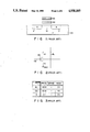
- the prior memory cell based on the double gate type transistor is illustrated in cross-sectional form in FIG. 1.
- source region S and drain region D are separately formed in the surface region of P type semiconductor substrate 50.
- Channel region 51 is located between source and drain regions S and D.
- a first gate insulating film (not shown) is formed on channel region 51.
- Floating gate electrode 52 made of polycrystalline silicon, for example, is further formed on the first gate insulating film.
- a second gate insulating film (not shown) is formed on floating gate electrode 52.
- Control gate electrode 53 which is made of polycrystalline silicon, is laid on the second gate insulating film.
- the memory cell thus structured can be electrically depicted as an equivalent circuit, as shown in FIG. 2.
- a bit line BL is connected to the drain region D of transistor 60 used as a memory cell.
- the control gate electrode 53 is connected to control gate line CG.
- the source region S is connected to ground GND.
- the memory cell thus arranged operates in three modes, write, erase, and read modes. These operation modes, and voltages at the source region S, bit line BL and control gate line CG, are tabulated as in FIG. 3.
- the write mode will first be described.
- This mode is called an electron injection mode.
- electrons are injected into floating gate electrode 52 to raise the threshold voltage of cell transistor 60.
- an intensive electric field is concentrated in the depletion layer, which is formed particularly in the vicinity of the drain region D. Electrons travel from the source region S of transistor 60 toward drain region D. The electrons toward the drain region D are accelerated by the electric field concentrated near the drain region D, and gain enough energy to jump over the energy barrier of the first gate insulating film (not shown), from the surface of substrate 50. This type of electrons are called hot electrons.
- the hot electrons are attracted by the high voltage applied to the control gate electrode 53, and pass through the first gate insulating film, and enter into floating gate electrode 52, and are arrested there.
- the floating gate 52 is negatively charged, and in the region of the substrate under floating gate electrode 52, i.e., in the channel region 51, it is difficult for the inversion of conductivity or channel formation to occur.
- the threshold voltage of cell transistor 60 substantially rises.
- the data erase mode is also called an electron emission mode.
- the memory cells are radiated with ultraviolet rays.
- the radiated ultraviolet rays excite the electrons, which are injected into floating gate electrode 52 in the data write mode.
- the excited electrons jump over the energy barrier of the second insulating film (not shown) and enter into control gate electrode 53.
- the electrons also jump over the energy barrier of the first insulating film (not shown) to enter into substrate 50. Such flow of electrons reduces the threshold value of cell transistor 60.
- the threshold voltage of the cell transistor is large. Under this condition, no channel is formed between the source and drain regions, thereby prohibiting the flow of cell current.
- the bit line voltage is kept at 2V.
- the threshold voltage of cell transistor 60 is small. Therefore, a channel is formed between the source and drain regions, to allow the cell current to flow. Further, the bit line voltage drops to approximately 0V. In this way, when the data is read out, the bit line voltage change in accordance with whether or not electrons are injected into or emitted from floating gate electrode 52.
- the voltage change on the bit line is amplified by a sense amplifier (not shown). This provides logical "1" or "0" of the data as read out from cell transistor 60.
- the cell transistor in which no electrons are emitted When the cell transistor in which no electrons are emitted, is subjected to the read mode for a long time, electrons are injected little by little into floating gate electrode 52, so that the threshold voltage of the cell transistor gradually rises. After a predetermined period of time elapses, enough electrons have been injected into floating gate electrode 52 to invert the logical level of the data stored in the cell transistor. As a result, erroneous data will be read out from the cell transistor. Such a phenomenon is called a soft write (weak write). The characteristic of the soft write phenomenon with respect to the time lapse is called a read retention characteristic (data hold characteristic).
- the read retention characteristic is enhanced, by constraining the soft write phenomenon.
- a first problem is the complicated circuit of the sense amplifier. To fabricate such a complicated circuit into semiconductor chip, a large chip area is required, resulting in increase of cost to manufacture.
- a second problem is the reduced margin for the power voltage in the read mode. This is problematic particularly for the low voltage operation.
- a third problem is the need for the constant voltage source of 2V to be supplied to the bit line. The prior memory device must contain a circuit for forming such an intermediate voltage, resulting in increase of power consumption.
- the prior nonvolatile memory device involves many problems; the increased chip area, unstable low voltage operation, and increased power consumption.
- an object of this invention is to provide a nonvolatile memory device including the features of low voltage, low power consumption, high operating speed, and simple peripheral circuitry including the sense amplifier.
- a nonvolatile semiconductor memory device comprising a memory cell including a first conductivity type semiconductor substrate, first and second diffusion layers of a second conductivity type formed in said substrate, a channel region formed in the surface region of said substrate, which is located between said first and second diffusion layers, a floating gate electrode provided on said channel region, a control gate electrode provided on said floating gate electrode, and means for lessening an electric field concentration occurred between said first layer and said channel region, a control gate line for supplying predetermined voltages to said control gate electrode in a read mode and a write mode, a read line for supplying predetermined voltages to said first diffusion layer in the read and write modes, and a write line for supplying predetermined voltages to said second diffusion layer in the read and write modes.
- a nonvolatile semiconductor memory device comprising a memory cell including a first conductivity type semiconductor substrate, first and second diffusion layers of a second conductivity type formed in said substrate, a channel region formed in the surface region of said substrate and located between said first and second diffusion layers, a floating gate electrode provided on said channel region, a control gate electrode provided on said floating gate electrode, and means for preventing the carriers generated in the vicinity of said first diffusion layer in said channel region from being injected into said floating gate electrode, a control gate line for supplying predetermined voltages to said control gate electrode in a read mode and a write mode, a read line for supplying predetermined voltages to said first diffusion layer in the read and write modes, and a write line for supplying predetermined voltages to said second diffusion layer in the read and write modes.
- the voltage is applied to the memory cell in such a manner that the current flowing between the first and second diffusion layers as the source and drain has the direction, which is reversed when the mode is changed from the read mode to the write mode and vice versa.
- means for lessening the electric field concentration is provided in the first diffusion layer in which the electric field is concentrated in the read mode.
- another means is provided for blocking the injection of carriers generated near the first diffusion layer into the floating gate.
- FIG. 1 shows a cross-sectional view of a conventional nonvolatile semiconductor memory cell of double gate type
- FIG. 2 shows a circuit diagram equivalent to the semiconductor memory cell shown in FIG. 1;
- FIG. 3 shows values of voltages applied to the memory cell of FIG. 2, in the write, erase and read modes
- FIG. 4 shows a schematic cross-sectional view of a memory cell used for a nonvolatile semiconductor memory of the present invention
- FIG. 5 shows a circuit diagram equivalent to the semiconductor memory cell shown in FIG. 4;
- FIG. 6 shows values of voltages applied to the memory cell of FIG. 5, in the write, erase and read modes
- FIGS. 7 to 10 show cross sectional views of specific structures of the memory cell shown in FIG. 4, respectively;
- FIG. 11 shows a circuit diagram of a cell array of a nonvolatile semiconductor memory of the present invention, formed by the plural memory cells shown in FIG. 4;
- FIGS. 12 to 14 show circuit diagrams of read/write circuits used for the cell array shown in FIG. 11, respectively;
- FIG. 15 shows signal charts at various portions of the read/write circuit shown in FIG. 14;
- FIG. 16 shows a circuit diagram of another read/write circuit used for the cell array shown in FIG. 11;
- FIG. 17 shows signal charts at various portions of the read/write circuit shown in FIG. 16.
- FIG. 18 shows a circuit diagram modified from the read/write circuit shown in FIG. 12, in which some of the parts are shown in block or symbol form.
- a semiconductor memory cell which is used for a nonvolatile semiconductor memory device according to this invention, is illustrated in cross-sectional form in FIG. 4.
- source region 11 and drain region 12, as N type diffusion layers, are separately formed in the surface region of P type semiconductor substrate 10.
- Channel region 13 is located between diffusion layers 11 and 12.
- a first gate insulating film (not shown) is formed on channel region 13.
- Floating gate electrode 14 made of polycrystalline silicon, for example, is further formed on the first gate insulating film.
- a second gate insulating film (not shown) is formed on floating gate electrode 14.
- Control gate electrode 15, which is made of polycrystalline silicon, is laid on the second gate insulating film.
- a means for lessening the electric field concentration between diffusion layer 11 and channel region 13 is provided in at least the portion of diffusion layer 11 which is in contact with channel region 13.
- the same portion is provided with a means for blocking the flow of hot electrons generated in the portion of channel region 13, near diffusion layer 11, to floating gate electrode 14. This means is denoted as 16 in FIG. 4.
- transistor 20 serves as a memory cell of the memory device, and has a structure as shown in FIG. 4.
- the diffusion layer 11 of transistor 20 is coupled with read line RL, and the diffusion layer 12 is connected to write line WL.
- the control electrode 15 of transistor 20 is connected to control gate line CG.
- the memory cell thus arranged operates in three modes, write, erase, and read modes, as in the prior art. These operation modes, and voltages at the read line RL write line WL and control gate line CG, are tabulated in FIG. 6.
- the write mode (electron injection mode) will first be described.
- electrons are injected into floating gate electrode 14 to raise the threshold voltage of cell transistor 20.
- the high voltage of 12.5 V is applied between the diffusion layers 11 and 12 of the cell 20, and electrons move from diffusion layer 11 to diffusion layer 12.
- an intensive electric field is concentrated in the depletion layer, which is formed in the vicinity of the diffusion layer 12 in the channel region.
- the electrons toward the drain region D are accelerated by the concentrated electric field, and gain enough energy to jump over the energy barrier of the first gate insulating film (not shown), from the surface of substrate 10.
- the hot electrons are attracted by the high voltage applied to the control gate electrode 15, pass through the first gate insulating film, enter floating gate electrode 14, and are trapped there. As a result, the threshold voltage of cell transistor 20 rises.
- the memory cells are radiated with ultraviolet rays.
- the radiated ultraviolet rays excite the electrons, which are injected into floating gate electrode 14 in the data write mode.
- the excited electrons jump over the energy barrier of the second insulating film (not shown) and enter control gate electrode 15.
- the electrons also jump over the energy barrier of the first insulating film (not shown) to enter into substrate 10. Such flow of electrons reduces the threshold value of cell transistor 20.
- the threshold voltage of the cell transistor is large. Under this condition, no channel is formed between the source and drain regions, thereby prohibiting the cell current flow.
- the read line voltage is kept at 5V.
- the threshold voltage of cell transistor 20 is small. Therefore, the cell current flows between read line RL and write line WL.
- the voltage on read line RL drops to approximately 0V.
- the voltage difference between 5V and 0V on read line RL is amplified by a sense amplifier (not shown) connected to this read line. This provides logical "1" or "0" of the data as read out from cell transistor 20.
- the normal read power voltage of 5V is directly applied to read line RL. Even though the 5V is applied to the read line, the soft write phenomenon can be prevented and the read retention characteristic can be significantly improved.
- This advantageous feature is due to the means 16 to lessen the electric field concentration or the hot electron blocking means 16 as already mentioned. With the provision of such means, the generation of hot electrons is constrained in the vicinity of the diffusion layer 11 in contact with channel region 13 or the hot electrons, if generated, can be prevented from being injected into floating gate electrode 14. Therefore, if the memory cell is subjected to the read mode for a long time, the injection of electrons into floating gate electrode 14 is minimized, providing a significant improvement of the read retention characteristic.
- the cell transistor with the means 16 can practically be realized as shown in FIGS. 7 to 10.
- the devices of FIGS. 7 and 8 use the means for lessening the electric field concentration in the vicinity of the diffusion layer 11 in the channel region 13.
- N-type diffusion layer 17 is formed in the surface region of substrate 10, with one side of the layer 17 in contact with diffusion layer 11, and the other side in contact with channel region 13.
- the impurity concentration of diffusion layer 17 serving as means 16 is lower than that of diffusion layer 11.
- N-type diffusion layer 18 serving as the means 16 is provided surrounding the diffusion layer 11 in the surface region of substrate 10 as shown.
- the impurity concentration of diffusion layer 18 serving as means 16 is lower than that of diffusion layer 11.
- the means 16 functions to prevent the hot electrons from being injected into floating gate electrode 14.
- insulating film 19 is formed on the portions of the surfaces of substrate 10 and diffusion layer 11, where diffusion layer 11 contacts channel region 13. One side of the film 19 is in contact with the surface portions, while the other side of the film 19 partially contacts the lower side (as viewed in the drawing) of floating gate electrode 14. The thickness of the film 19 is thicker than that of the remaining portion. This insulating film 19 may be replaced by an insulating film considerably impeding electrons as carriers passing therethrough.
- Control gate 15 is laid in part above floating gate electrode 14, and bends downwardly (as viewed in the drawing) to extend over the channel region surface above which the gate 14 is not laid. This extended portion of control gate electrode 15 is used as the means 16.
- the electric field can be concentrated in the vicinity of diffusion layer 12 in channel region 13, in the write mode. A sufficient number of electrons can be injected into floating gate electrode 14.
- the electric field concentration near the diffusion layer 11 in channel region 13 is lessened to limit the generation of electrons to be injected into floating gate electrode 14, or to block the injection of electrons into floating gate electrode 14. As a result, the read retention characteristic is improved.
- FIG. 11 there is shown a cell array of an EPROM made up of cell transistors of the type, which belongs to any of the FIGS. 7 to 10 transistor types. As shown, these cell transistors are arranged in a matrix fashion. A plurality of parallel arrayed read lines RLm, RLn and RLo are provided extending in column direction. Write lines WLm, WLn, and WLo are also arrayed in parallel and extend in the column direction. These read and write lines are alternately arranged. A plurality of control gate lines CGi, CGj and CGk are parallel arrayed and extend in the row direction. One read line RLm, for example, is connected to the sources of cell transistors linearly arrayed along that read line.
- the write line WLm adjacent to the read line RLm is connected to the drains of cell transistors 20 on the same column.
- One control gate line CGi is connected to the control gates of cell transistors linearly arrayed in the row of the matrix array and along that control gate line CGi.
- the remaining control gate lines CGj and CGk are connected to the cell transistors in a similarly fashion.
- FIG. 12 shows a circuit diagram of a read/write circuit for the memory cell array of FIG. 11.
- memory cell array 20 is one of the matrix arrayed cell transistors as shown in FIG. 11.
- a switching transistor 31 as a P channel MOS transistor and load resistor 30 are connected in series between read line RL and power source Vcc.
- Another switching transistor 32 as an N channel MOS transistor is connected between read line RL and ground GND.
- a write control signal is connected to the gates of these switching transistors 31 and 32. The write control signal is 5V in the write mode, and 0V in the read mode.
- Read line RL is connected to the input terminal of sense amplifier 33.
- the write control signal is set at 5V.
- P channel MOS transistor 31 is nonconductive, and N channel MOS transistor 32 is conductive.
- read line RL is connected to ground GND via transistor 32 and set at 0V.
- Write line WL and control gate line CG are set at 12.5V. Under this condition, electrons are injected into the floating gate electrode of cell transistor 20 in the manner as previously mentioned referring to FIGS. 4 to 6.
- the write control signal is set at 0V
- MOS transistor 31 is conductive while MOS transistor 32 is nonconductive.
- read line RL is set at 5V. The sum Rr of conduction resistance of transistor 31 and resistance of resistor 30 is given by
- Roff indicates the resistance between the read and write lines RL and WL when electrons are being injected into the floating gate electrode of memory cell 20, and Ron indicates the resistance between those lines RL and WL when electrons are being emitted from the same gate electrode.
- the voltage setting ranges of the FIG. 12 circuit are: 0V to 12.5V (high voltage system) for WL, 5V to 12.5V (high and low voltage systems) for CG, and 0V to 5V (low voltage system) for RL.
- the signal line used for both high and low voltage systems is only CG.
- the remaining signal lines WL and RL are used for the high voltage system and the low voltage system, respectively.
- This fact implies that the peripheral circuit for processing these signals is very simple. In other words, the peripheral circuit can be separated into the high voltage system and the low voltage system, simplifying the circuit arrangement.
- FIG. 13 shows another example of a read/write circuit for the FIG. 11 memory array.
- This read/write circuit differs with respect to the load circuit for the read line RL.
- the load circuit contains a single component, P channel MOS transistor 34, while the FIG. 12 circuit contains two components, P channel MOS transistor 31 and resistor 30. Accordingly, the resistance Rr in the relation (1) only comprises the conduction resistance of transistor 34.
- the channel dimension of transistor 34 is adjusted so as to satisfy the relation (1).
- FIG. 14 shows another example of a read/write circuit for the FIG. 11 memory array.
- This example is a modification of the FIG. 13 circuit and includes OR gate 35 placed between the gate of load transistor 34 and the terminal for the write control signal.
- the OR gate 35 allows the write control signal to pass therethrough, while being timed by clock signal ⁇ .
- the write control signal is 0V in the read mode. Therefore, when clock signal ⁇ is 0V, transistor 34 is conductive.
- the read current flows through write line WL in the read mode, which is derived from power source Vcc and applied to write line WL via read line RL and memory cell 20. This results in a further reduction of power consumption.
- FIG. 16 shows a further example of the read/write circuit.
- the FIG. 16 circuit is a modification of the FIG. 14 circuit.
- AND gate 36 is inserted between the control gate line CG and the gate of cell transistor 20.
- AND gate 36 is controlled by the output of OR gate 35, so that the application of the control gate signal to cell transistor 20 is under control by clock signal ⁇ through OR gate 35.
- load transistor 34 is turned on to precharge read line RL to Vcc.
- the output of AND gate 36 is 0V, and the memory cell transistor 20 supplied with this voltage is nonconductive. Under this condition, no DC current flows from power source Vcc to write line via read line RL and cell 20.
- FIG. 18 shows a schematic illustration of a read/write circuit for the memory cell array.
- load 40 as illustrated in block form contains the switching transistor (31 or 34 in FIGS. 12 to 16) and/or load resistor (30 in FIG. 12).
- Inverter 33 is used in place of the sense amplifier (33 in FIGS. 12 to 16).
- the read line potential can be set to the extreme values, 0V and 5V, respectively in the read and write mode. Therefore, there is no need for the amplifying means, such as the sense amplifier, for amplifying the minute voltage difference.
- the sense amplifier which is essential to the conventional circuit, may be replaced by a mere inverter designated as 33 in FIG. 18. This feature simplifies the circuit arrangement of the sense amplifier circuit, and reduces the access time.
- the semiconductor memory device is operable at high speed, and with low power dissipation, and with simple peripheral circuit including the sense amplifier circuit.
Landscapes
- Engineering & Computer Science (AREA)
- Microelectronics & Electronic Packaging (AREA)
- Read Only Memory (AREA)
- Non-Volatile Memory (AREA)
- Semiconductor Memories (AREA)
Applications Claiming Priority (2)
| Application Number | Priority Date | Filing Date | Title |
|---|---|---|---|
| JP62-87482 | 1987-04-09 | ||
| JP62087482A JPS63252481A (ja) | 1987-04-09 | 1987-04-09 | 不揮発性半導体メモリ |
Publications (1)
| Publication Number | Publication Date |
|---|---|
| US4930105A true US4930105A (en) | 1990-05-29 |
Family
ID=13916159
Family Applications (1)
| Application Number | Title | Priority Date | Filing Date |
|---|---|---|---|
| US07/178,609 Expired - Lifetime US4930105A (en) | 1987-04-09 | 1988-04-07 | Nonvolatile semiconductor memory device with a double gate structure |
Country Status (5)
| Country | Link |
|---|---|
| US (1) | US4930105A (de) |
| EP (1) | EP0286121B1 (de) |
| JP (1) | JPS63252481A (de) |
| KR (1) | KR910007401B1 (de) |
| DE (1) | DE3876666T2 (de) |
Cited By (11)
| Publication number | Priority date | Publication date | Assignee | Title |
|---|---|---|---|---|
| US5017978A (en) * | 1989-03-31 | 1991-05-21 | U.S. Philips Corp. | EPROM having a reduced number of contacts |
| US5032881A (en) * | 1990-06-29 | 1991-07-16 | National Semiconductor Corporation | Asymmetric virtual ground EPROM cell and fabrication method |
| US5058062A (en) * | 1988-11-09 | 1991-10-15 | Kabushiki Kaisha Toshiba | Nonvolatile semiconductor memory circuit including a reliable sense amplifier |
| US5241498A (en) * | 1989-07-05 | 1993-08-31 | Kabushiki Kaisha Toshiba | Non-volatile semiconductor memory device |
| US5341329A (en) * | 1988-12-28 | 1994-08-23 | Kabushiki Kaisha Toshiba | Nonvolatile semiconductor memory device capable of preventing read error caused by overerase state and method therefor |
| US5396458A (en) * | 1991-10-21 | 1995-03-07 | Rohm Co., Ltd. | Semiconductor memory device and method of writing and reading out information for the same |
| US5617352A (en) * | 1995-12-13 | 1997-04-01 | The United States Of America As Represented By The Secretary Of The Navy | Non-volatile, bidirectional, electrically programmable integrated memory element implemented using double polysilicon |
| US5736891A (en) * | 1996-01-11 | 1998-04-07 | International Business Machines Corporation | Discharge circuit in a semiconductor memory |
| US5862076A (en) * | 1990-11-13 | 1999-01-19 | Waferscale Integration, Inc. | Fast EPROM array |
| US6480422B1 (en) | 2001-06-14 | 2002-11-12 | Multi Level Memory Technology | Contactless flash memory with shared buried diffusion bit line architecture |
| US8320191B2 (en) | 2007-08-30 | 2012-11-27 | Infineon Technologies Ag | Memory cell arrangement, method for controlling a memory cell, memory array and electronic device |
Families Citing this family (3)
| Publication number | Priority date | Publication date | Assignee | Title |
|---|---|---|---|---|
| JP3059442B2 (ja) * | 1988-11-09 | 2000-07-04 | 株式会社日立製作所 | 半導体記憶装置 |
| JP3522788B2 (ja) * | 1992-10-29 | 2004-04-26 | 株式会社ルネサステクノロジ | 半導体集積回路装置 |
| EP0926686A1 (de) * | 1997-12-23 | 1999-06-30 | STMicroelectronics S.r.l. | Nichtflüchtiger Seriell-Flash-, EPROM-, EEPROM-, und Flash-EEPROM-Speicher in AMG-Konfiguration |
Citations (11)
| Publication number | Priority date | Publication date | Assignee | Title |
|---|---|---|---|---|
| US4448400A (en) * | 1981-07-13 | 1984-05-15 | Eliyahou Harari | Highly scalable dynamic RAM cell with self-signal amplification |
| US4467453A (en) * | 1979-09-04 | 1984-08-21 | Texas Instruments Incorporated | Electrically programmable floating gate semiconductor memory device |
| EP0143596A2 (de) * | 1983-11-24 | 1985-06-05 | Fujitsu Limited | Programmierbare Festwertspeicheranordnung |
| EP0183235A2 (de) * | 1984-11-26 | 1986-06-04 | Kabushiki Kaisha Toshiba | Nichtflüchtige Halbleiterspeicheranordnung |
| US4652897A (en) * | 1984-07-13 | 1987-03-24 | Hitachi, Ltd. | Semiconductor memory device |
| US4725980A (en) * | 1984-11-20 | 1988-02-16 | Fujitsu Limited | Read only memory circuit |
| US4754320A (en) * | 1985-02-25 | 1988-06-28 | Kabushiki Kaisha Toshiba | EEPROM with sidewall control gate |
| US4788663A (en) * | 1987-04-24 | 1988-11-29 | Kabushiki Kaisha Toshiba | Nonvolatile semiconductor memory device with a lightly-doped drain structure |
| US4794565A (en) * | 1986-09-15 | 1988-12-27 | The Regents Of The University Of California | Electrically programmable memory device employing source side injection |
| US4812898A (en) * | 1985-06-21 | 1989-03-14 | Nec Corporation | Electronically programmable and erasable memory device having floating gate electrode with a unique distribution of impurity concentration |
| US4870615A (en) * | 1987-01-31 | 1989-09-26 | Kabushiki Kaisha Toshiba | Nonvolatile floating gate semiconductor memory device |
Family Cites Families (2)
| Publication number | Priority date | Publication date | Assignee | Title |
|---|---|---|---|---|
| US4258378A (en) * | 1978-05-26 | 1981-03-24 | Texas Instruments Incorporated | Electrically alterable floating gate memory with self-aligned low-threshold series enhancement transistor |
| US4698787A (en) * | 1984-11-21 | 1987-10-06 | Exel Microelectronics, Inc. | Single transistor electrically programmable memory device and method |
-
1987
- 1987-04-09 JP JP62087482A patent/JPS63252481A/ja active Pending
-
1988
- 1988-04-07 US US07/178,609 patent/US4930105A/en not_active Expired - Lifetime
- 1988-04-08 DE DE8888105638T patent/DE3876666T2/de not_active Expired - Lifetime
- 1988-04-08 EP EP88105638A patent/EP0286121B1/de not_active Expired - Lifetime
- 1988-04-08 KR KR1019880003982A patent/KR910007401B1/ko not_active Expired
Patent Citations (11)
| Publication number | Priority date | Publication date | Assignee | Title |
|---|---|---|---|---|
| US4467453A (en) * | 1979-09-04 | 1984-08-21 | Texas Instruments Incorporated | Electrically programmable floating gate semiconductor memory device |
| US4448400A (en) * | 1981-07-13 | 1984-05-15 | Eliyahou Harari | Highly scalable dynamic RAM cell with self-signal amplification |
| EP0143596A2 (de) * | 1983-11-24 | 1985-06-05 | Fujitsu Limited | Programmierbare Festwertspeicheranordnung |
| US4652897A (en) * | 1984-07-13 | 1987-03-24 | Hitachi, Ltd. | Semiconductor memory device |
| US4725980A (en) * | 1984-11-20 | 1988-02-16 | Fujitsu Limited | Read only memory circuit |
| EP0183235A2 (de) * | 1984-11-26 | 1986-06-04 | Kabushiki Kaisha Toshiba | Nichtflüchtige Halbleiterspeicheranordnung |
| US4754320A (en) * | 1985-02-25 | 1988-06-28 | Kabushiki Kaisha Toshiba | EEPROM with sidewall control gate |
| US4812898A (en) * | 1985-06-21 | 1989-03-14 | Nec Corporation | Electronically programmable and erasable memory device having floating gate electrode with a unique distribution of impurity concentration |
| US4794565A (en) * | 1986-09-15 | 1988-12-27 | The Regents Of The University Of California | Electrically programmable memory device employing source side injection |
| US4870615A (en) * | 1987-01-31 | 1989-09-26 | Kabushiki Kaisha Toshiba | Nonvolatile floating gate semiconductor memory device |
| US4788663A (en) * | 1987-04-24 | 1988-11-29 | Kabushiki Kaisha Toshiba | Nonvolatile semiconductor memory device with a lightly-doped drain structure |
Cited By (12)
| Publication number | Priority date | Publication date | Assignee | Title |
|---|---|---|---|---|
| US5058062A (en) * | 1988-11-09 | 1991-10-15 | Kabushiki Kaisha Toshiba | Nonvolatile semiconductor memory circuit including a reliable sense amplifier |
| US5341329A (en) * | 1988-12-28 | 1994-08-23 | Kabushiki Kaisha Toshiba | Nonvolatile semiconductor memory device capable of preventing read error caused by overerase state and method therefor |
| US5017978A (en) * | 1989-03-31 | 1991-05-21 | U.S. Philips Corp. | EPROM having a reduced number of contacts |
| US5241498A (en) * | 1989-07-05 | 1993-08-31 | Kabushiki Kaisha Toshiba | Non-volatile semiconductor memory device |
| US5032881A (en) * | 1990-06-29 | 1991-07-16 | National Semiconductor Corporation | Asymmetric virtual ground EPROM cell and fabrication method |
| US5862076A (en) * | 1990-11-13 | 1999-01-19 | Waferscale Integration, Inc. | Fast EPROM array |
| US5396458A (en) * | 1991-10-21 | 1995-03-07 | Rohm Co., Ltd. | Semiconductor memory device and method of writing and reading out information for the same |
| US5617352A (en) * | 1995-12-13 | 1997-04-01 | The United States Of America As Represented By The Secretary Of The Navy | Non-volatile, bidirectional, electrically programmable integrated memory element implemented using double polysilicon |
| US5736891A (en) * | 1996-01-11 | 1998-04-07 | International Business Machines Corporation | Discharge circuit in a semiconductor memory |
| US6480422B1 (en) | 2001-06-14 | 2002-11-12 | Multi Level Memory Technology | Contactless flash memory with shared buried diffusion bit line architecture |
| US8320191B2 (en) | 2007-08-30 | 2012-11-27 | Infineon Technologies Ag | Memory cell arrangement, method for controlling a memory cell, memory array and electronic device |
| US9030877B2 (en) | 2007-08-30 | 2015-05-12 | Infineon Technologies Ag | Memory cell arrangement, method for controlling a memory cell, memory array and electronic device |
Also Published As
| Publication number | Publication date |
|---|---|
| EP0286121A2 (de) | 1988-10-12 |
| EP0286121A3 (en) | 1989-05-10 |
| JPS63252481A (ja) | 1988-10-19 |
| EP0286121B1 (de) | 1992-12-16 |
| DE3876666T2 (de) | 1993-04-22 |
| KR880013174A (ko) | 1988-11-30 |
| KR910007401B1 (ko) | 1991-09-25 |
| DE3876666D1 (de) | 1993-01-28 |
Similar Documents
| Publication | Publication Date | Title |
|---|---|---|
| US4870615A (en) | Nonvolatile floating gate semiconductor memory device | |
| US5392253A (en) | Nonvolatile semiconductor memory device having row decoder supplying a negative potential to word lines during erase mode | |
| US5350938A (en) | Nonvolatile semiconductor memory circuit with high speed read-out | |
| US6657893B2 (en) | Nonvolatile semiconductor memory device and method for driving the same | |
| US4930105A (en) | Nonvolatile semiconductor memory device with a double gate structure | |
| JP2001217328A (ja) | 半導体デバイスを動作させる方法 | |
| KR100712087B1 (ko) | 반도체메모리장치및그제조방법 | |
| KR900009176B1 (ko) | 불휘발성 반도체메모리 | |
| JP2000113683A (ja) | 半導体装置 | |
| KR930000816B1 (ko) | 불휘발성 반도체메모리 | |
| JP3231437B2 (ja) | 不揮発性半導体記憶装置 | |
| US4982377A (en) | Erasable programmable read only memory device improved in operation speed and in the amount of read out current | |
| US7042763B1 (en) | Programming method for nonvolatile memory cell | |
| EP0376290B1 (de) | Nichtflüchtige Halbleiterspeicheranordnung, fähig um einen durch einen Überlöschungszustand verursachten Lesefehler zu verhindern | |
| US5050124A (en) | Semiconductor memory having load transistor circuit | |
| JPS6244702B2 (de) | ||
| KR960011187B1 (ko) | 불휘발성 반도체메모리 | |
| US5134450A (en) | Parallel transistor circuit with non-volatile function | |
| JP3104978B2 (ja) | 不揮発性半導体記憶装置の制御方法 | |
| JPS6295875A (ja) | 半導体記憶装置 | |
| JPH0370879B2 (de) | ||
| JPH0793018B2 (ja) | 不揮発性半導体メモリ | |
| JP2003173689A (ja) | 不揮発性半導体記憶装置 | |
| JPH11135653A (ja) | 不揮発性半導体記憶装置 | |
| JPH0430754B2 (de) |
Legal Events
| Date | Code | Title | Description |
|---|---|---|---|
| AS | Assignment |
Owner name: KABUSHIKI KAISHA TOSHIBA, 72 HORIKAWA-CHO, SAIWAI- Free format text: ASSIGNMENT OF ASSIGNORS INTEREST.;ASSIGNORS:MATSUMOTO, OSAMU;MARUYAMA, TADASHI;MURATA, HIROYOSHI;AND OTHERS;REEL/FRAME:004896/0134;SIGNING DATES FROM 19880329 TO 19880330 |
|
| STCF | Information on status: patent grant |
Free format text: PATENTED CASE |
|
| FEPP | Fee payment procedure |
Free format text: PAYOR NUMBER ASSIGNED (ORIGINAL EVENT CODE: ASPN); ENTITY STATUS OF PATENT OWNER: LARGE ENTITY |
|
| FPAY | Fee payment |
Year of fee payment: 4 |
|
| FPAY | Fee payment |
Year of fee payment: 8 |
|
| FPAY | Fee payment |
Year of fee payment: 12 |