US4991003A - Receiver with correction for comb filter frequency response - Google Patents
Receiver with correction for comb filter frequency response Download PDFInfo
- Publication number
- US4991003A US4991003A US07/341,017 US34101789A US4991003A US 4991003 A US4991003 A US 4991003A US 34101789 A US34101789 A US 34101789A US 4991003 A US4991003 A US 4991003A
- Authority
- US
- United States
- Prior art keywords
- comb filter
- input
- output
- correction circuit
- receiver
- Prior art date
- Legal status (The legal status is an assumption and is not a legal conclusion. Google has not performed a legal analysis and makes no representation as to the accuracy of the status listed.)
- Expired - Lifetime
Links
- 238000012937 correction Methods 0.000 title claims abstract description 39
- 239000003990 capacitor Substances 0.000 claims description 3
- 230000001419 dependent effect Effects 0.000 claims description 3
- 230000008878 coupling Effects 0.000 claims 5
- 238000010168 coupling process Methods 0.000 claims 5
- 238000005859 coupling reaction Methods 0.000 claims 5
- 230000001747 exhibiting effect Effects 0.000 claims 1
- 230000008901 benefit Effects 0.000 abstract description 7
- 241000023320 Luma <angiosperm> Species 0.000 description 12
- 238000002955 isolation Methods 0.000 description 12
- OSWPMRLSEDHDFF-UHFFFAOYSA-N methyl salicylate Chemical compound COC(=O)C1=CC=CC=C1O OSWPMRLSEDHDFF-UHFFFAOYSA-N 0.000 description 12
- 239000011521 glass Substances 0.000 description 8
- 230000003111 delayed effect Effects 0.000 description 4
- 238000010586 diagram Methods 0.000 description 4
- 230000000694 effects Effects 0.000 description 3
- 238000006842 Henry reaction Methods 0.000 description 2
- 239000002131 composite material Substances 0.000 description 2
- 238000004519 manufacturing process Methods 0.000 description 2
- 238000000926 separation method Methods 0.000 description 2
- 230000000903 blocking effect Effects 0.000 description 1
- 238000006243 chemical reaction Methods 0.000 description 1
- 230000007423 decrease Effects 0.000 description 1
- 238000006073 displacement reaction Methods 0.000 description 1
- 230000008030 elimination Effects 0.000 description 1
- 238000003379 elimination reaction Methods 0.000 description 1
- 238000003908 quality control method Methods 0.000 description 1
- 230000000630 rising effect Effects 0.000 description 1
- 230000000087 stabilizing effect Effects 0.000 description 1
- 230000000007 visual effect Effects 0.000 description 1
Images




Classifications
-
- H—ELECTRICITY
- H04—ELECTRIC COMMUNICATION TECHNIQUE
- H04N—PICTORIAL COMMUNICATION, e.g. TELEVISION
- H04N9/00—Details of colour television systems
- H04N9/77—Circuits for processing the brightness signal and the chrominance signal relative to each other, e.g. adjusting the phase of the brightness signal relative to the colour signal, correcting differential gain or differential phase
-
- H—ELECTRICITY
- H04—ELECTRIC COMMUNICATION TECHNIQUE
- H04N—PICTORIAL COMMUNICATION, e.g. TELEVISION
- H04N9/00—Details of colour television systems
- H04N9/64—Circuits for processing colour signals
- H04N9/646—Circuits for processing colour signals for image enhancement, e.g. vertical detail restoration, cross-colour elimination, contour correction, chrominance trapping filters
-
- H—ELECTRICITY
- H04—ELECTRIC COMMUNICATION TECHNIQUE
- H04N—PICTORIAL COMMUNICATION, e.g. TELEVISION
- H04N9/00—Details of colour television systems
- H04N9/77—Circuits for processing the brightness signal and the chrominance signal relative to each other, e.g. adjusting the phase of the brightness signal relative to the colour signal, correcting differential gain or differential phase
- H04N9/78—Circuits for processing the brightness signal and the chrominance signal relative to each other, e.g. adjusting the phase of the brightness signal relative to the colour signal, correcting differential gain or differential phase for separating the brightness signal or the chrominance signal from the colour television signal, e.g. using comb filter
Definitions
- This invention relates to television receivers of the type employing comb filters for providing luminance and chrominance signal separation and particularly to receivers in which the comb filter exhibits a non-uniform amplitude response with frequency and in which a compensation circuit is provided for reducing the response variations.
- a conventional comb filter includes a delay device for imparting a one horizontal line (1-H) delay to the video input signal, an adder for adding the delayed and non-delayed input signals to provide a luminance output signal and a subtractor for subtracting the delayed and non-delayed signals to provide a chrominance output signal.
- the delay element used in a comb filter has a very significant effect on the comb filter frequency response characteristic.
- the ideal delay element would have a constant delay independent of frequency thereby providing a linear phase response and thus a uniform amplitude response throughout the video frequency band to be filtered.
- the delay element presently closest to this ideal is the digital delay line employing binary storage elements. Unfortunately, digital delay lines are costly and relatively complex because video signals are conventionally received in analog form and so conversion to digital form is necessary to use digital delay lines of the binary storage type.
- Analog delay elements such as glass delay lines
- Comb filters employing glass delay elements are however subject to delay variations with frequency (i.e., non-linear phase response) and thus the overall amplitude response of such comb filters tends to vary with frequency.
- amplitude response 2 of FIG. 2 herein illustrates the uncorrected response of a commercially available comb filter employing a glass delay line. As shown, the uncorrected response exhibits a rising response from about 2.5 MHz to 4.5 MHz with a peak of about +6 dB.
- the manufacture of this filter has included a correction circuit having the characteristic shown by response 3. The resultant corrected response is illustrated by curve 4.
- the amplitude corrected comb filtered signal (4) exhibits a dip of about 2 dB at a frequency of about 2.5 MHz, it returns to zero dB at about 3 MHz and decreases thereafter.
- the rather large 6 dB variation of the uncorrected comb filter has been reduced to only 2 dB by internal correction circuits provided by the manufacturer (TDK Incorporated, model HCF0020C).
- the comb filter correction (to 2 dB) provided by the filter manufacturer is quite good considering the rather large (+6 dB) variations typical of uncompensated comb filters with glass delay lines. It has been recognized by the present inventor, however, that it would be desirable to provide a further correction of the comb filter response to reduce the luminance signal variations to a few tenths of a decibel in the luminance frequency range. To this end the present inventor has previously designed a receiver in which an auxiliary luminance amplitude correction circuit was included which achieved this goal. This receiver has been manufactured and sold under the brand name "RCA" in receivers employing chassis identification numbers CTC 148/149 and is shown herein as FIG. 1 (PRIOR ART). An understanding of this prior art receiver (10) is helpful to appreciating the subtle nature of the present invention and so this receiver will now be described in detail.
- the chrominance signal C1 is applied to a first input 24 of a luminance-chrominance (Y-C) processor 26.
- the luminance signal Yl is applied to a second (luminance) input 28 of processor 26 by means of a cascade connection comprising, in the exact order named of: a contrast control 30, a luminance/chrominance delay correction circuit 32 having source (R1) and termination (R2) resistors and a comb filter correction circuit 34 (outlined in phantom).
- Processor 26 includes conventional circuits for providing functions such as chroma demodulation, hue and saturation control and matrixing for providing a suitable output regional (e.g., RGB) for display by display unit 36.
- the correction circuit 34 (outlined in phantom) comprises an input 40 connected to the output 38 of luma delay unit 32 (e.g., 300 nanoseconds) and an output 42 connected to input 28 of processor 26.
- Internally unit 34 includes a parallel resonant circuit comprising an inductor L1 and a capacitor C1 connected in common to terminals 40 and 42 at one end thereof and coupled to ground at the other end thereof by means of a resistor R3.
- Representative values for L1, C1 and R3 are 100 micro-Henrys, 39 pico-Farads and 8200 Ohms, respectively.
- This circuit provides the luma signal boost of about 2 dB shown in FIG. 2 as response 5 which flattens the overall response 6 to within less than 1 dB over the full luma band as shown.
- the present invention resides in: (1) discovery of the existence of the problem of image distortion in the prior art receiver, (2) discovery of the cause of the problem and (3) discovery of solutions which are both technically effective and cost effective.
- the cause of this problem has been found, in accordance with the present invention, to be related to the specific point in the prior art receiver 10 where the luminance signal amplitude correction circuit 34 is connected.
- the connection of circuit 34 has been discovered to cause reflections in delay line 32.
- the visual effect of these reflections or “ringing” is to create double images or ghosts of very short displacement relative to the main image and thus may be manifested visually as image blur.
- the technical reason that delay line 32 exhibits ringing is two fold.
- the delay correction circuit 34 exhibits a frequency dependent impedance variation because the impedance of elements L1 and C1 changes with frequency.
- the luminance delay circuit 32 is a conventional analog delay line and so is sensitive to variations in impedance of its source and load elements. With circuit 34 directly connected to the load resistor R2 of delay line 32 the effective load impedance thus varies with frequency thereby causing frequency dependent load variations for delay line 32.
- the receiver is provided with circuit means for preventing impedance variations of the comb filter correction circuit from causing reflections in the luma delay line.
- circuit means for preventing impedance variations of the comb filter correction circuit from causing reflections in the luma delay line.
- the reflections are prevented utilizing existing receiver components thus eliminating the need for an isolation amplifier.
- the comb filtered luminance signal amplitude correction is applied between the output of the video source (switch 14) and the input of the receiver comb filter (18).
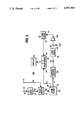
- FIG. 1 is a diagram in block and schematic form of a PRIOR ART receiver having correction for the response of a comb filter employing a glass delay line element;
- FIG. 2 is a response diagram of a PRIOR ART comb filter employing a glass delay element and illustrates response corrections used by a filter manufacturer and a receiver manufacturer to correct for amplitude errors of the comb filter;
- FIGS. 3, 4 and 5 are diagrams in block and schematic form of a television receiver embodying the invention.
- FIG. 6 is a diagram in block and schematic form of a preferred embodiment of a television receiver embodying the invention.
- the receiver 300 of FIG. 3, embodying the invention is similar to receiver 10 of FIG. 1 but differs in that a buffer or isolation amplifier 302 is interposed in the circuit path (30,32,34) between the output 20 of comb filter 18 and the luminance input 28 of Y-C processor 26.
- the amplifier 302 is connected between the output 38 of luma delay filter 32 and the input 40 of comb filter correction circuit 34. Accordingly, the impedance variations of comb filter correction circuit 34 are effectively isolated from the output of luma delay circuit 32 and thus the effective load impedance for circuit 32 is stabilized. This prevents reflections in line 32 and solves the newly discovered problem with the prior art receiver.
- the receiver 400 of FIG. 4, embodying the invention, is similar to receiver 10 of FIG. 1 but differs in three respects. Specifically, (1) the output 38 of luma delay line 32 is connected directly to the input 28 of processor 26 thus stabilizing the termination impedance of delay line 32. To provide comb filter frequency correction, a correction circuit 402 is connected at the output of contrast control 30. To prevent impedance variations of circuit 402 from varying the effective source impedance (R2) of luma delay line 32, an isolation or buffer amplifier 404 is connected between the output of comb correction circuit 402 and the source resistor R1 for luma delay circuit 32. The connection of load (termination) resistor R2 directly to input 28 of processor 26 eliminates load impedance variations. The use of isolation amplifier 404 prevents source impedance variations. Thus no reflections are produced in delay line 32 by impedance variations of correction circuit 402.
- the receiver 500 of FIG. 5 is similar to that of FIG. 4 except that comb filter correction and isolation is provided before contrast control 30. Specifically, the output 38 of delay line 32 is connected directly to the input 28 of Y-C processing unit 26 and a comb filter amplitude correction circuit 502 is connected to the comb filter output 20 and coupled via an isolation amplifier 504 to the input of the contrast control 30.
- the output connection of delay line 32 prevents load impedance variations.
- Comb filter correction is provided by relocating the correction circuit to the comb output 20.
- Source impedance variations are prevented by isolation amplifier 504. Accordingly, the load and source impedances of line 32 are constant and reflections are thereby suppressed.
- the receiver 600 of FIG. 6 is a presently preferred embodiment of the invention.
- This embodiment of the invention utilizes existing receiver circuits to solve the same newly discovered problem as the embodiments of FIGS. 3, 4 and 5 but this is achieved without requiring the use of an isolation amplifier. As previously explained, this provides two additional advantages of the invention including:
- the comb filter correction circuit is relocated. Specifically, the following changes have been made in the receiver 10 of FIG. 1 to implement receiver 600 of FIG. 6:
- the output 20 of video switch 14 is connected to input 40 of comb filter correction circuit 34 the output 42 of which is connected to the input of comb filter 18.
- the source and termination impedances of luminance signal delay line 32 are not influenced by impedance variations with frequency of the comb filter correction circuit 34 and thus the image blur problem is solved with the technical and economic advantages noted above.
- exemplary element values of L1, C1 and R3 are 47 micro-Henrys, 82 pico-Farads and 1500 Ohms, respectively.
- a series input resistor R5 e.g., 390 Ohms
- the L-C elements L1, C1 are coupled to a supply terminal 43 rather than to ground.
- the DC path thus provided (L1,R3,R5) advantageously provides DC bias to the input of comb filter 18 which employs an input amplifier biased by the video signal DC input component.
- the DC bias applied by correction circuit 34 eliminates the need for a separate bias network and blocking capacitor for comb filter 18.
Landscapes
- Engineering & Computer Science (AREA)
- Multimedia (AREA)
- Signal Processing (AREA)
- Processing Of Color Television Signals (AREA)
- Picture Signal Circuits (AREA)
- Filters That Use Time-Delay Elements (AREA)
Priority Applications (6)
| Application Number | Priority Date | Filing Date | Title |
|---|---|---|---|
| US07/341,017 US4991003A (en) | 1989-04-20 | 1989-04-20 | Receiver with correction for comb filter frequency response |
| CA002010665A CA2010665C (fr) | 1989-04-20 | 1990-02-22 | Recepteur a correction de l'effet du a la reponse frequentielle de filtre peigne |
| KR1019900005324A KR0159935B1 (ko) | 1989-04-20 | 1990-04-17 | 텔레비젼 수신기 |
| DE69023800T DE69023800T2 (de) | 1989-04-20 | 1990-04-18 | Empfänger mit Korrektur des Frequenzganges eines Kammfilters. |
| EP90304125A EP0394000B1 (fr) | 1989-04-20 | 1990-04-18 | Récepteur avec correction de la réponse en fréquence d'un filtre en peigne |
| JP2105110A JP2602116B2 (ja) | 1989-04-20 | 1990-04-19 | テレビジョン装置 |
Applications Claiming Priority (1)
| Application Number | Priority Date | Filing Date | Title |
|---|---|---|---|
| US07/341,017 US4991003A (en) | 1989-04-20 | 1989-04-20 | Receiver with correction for comb filter frequency response |
Publications (1)
| Publication Number | Publication Date |
|---|---|
| US4991003A true US4991003A (en) | 1991-02-05 |
Family
ID=23335923
Family Applications (1)
| Application Number | Title | Priority Date | Filing Date |
|---|---|---|---|
| US07/341,017 Expired - Lifetime US4991003A (en) | 1989-04-20 | 1989-04-20 | Receiver with correction for comb filter frequency response |
Country Status (6)
| Country | Link |
|---|---|
| US (1) | US4991003A (fr) |
| EP (1) | EP0394000B1 (fr) |
| JP (1) | JP2602116B2 (fr) |
| KR (1) | KR0159935B1 (fr) |
| CA (1) | CA2010665C (fr) |
| DE (1) | DE69023800T2 (fr) |
Cited By (3)
| Publication number | Priority date | Publication date | Assignee | Title |
|---|---|---|---|---|
| US5192996A (en) * | 1989-10-13 | 1993-03-09 | Matsushita Electric Industrial Co., Ltd. | Video chroma signal processing circuit |
| US6040727A (en) * | 1997-05-02 | 2000-03-21 | U.S. Philips Corporation | Delay device |
| US20170054952A1 (en) * | 2015-08-20 | 2017-02-23 | Qualcomm Incorporated | Systems and methods for configurable demodulation |
Citations (2)
| Publication number | Priority date | Publication date | Assignee | Title |
|---|---|---|---|---|
| US3728476A (en) * | 1971-03-17 | 1973-04-17 | Gen Electric | Luminance notch filter |
| US4677462A (en) * | 1985-11-07 | 1987-06-30 | Rca Corporation | Delay and filter network with chrominance trap between series input resistors |
Family Cites Families (3)
| Publication number | Priority date | Publication date | Assignee | Title |
|---|---|---|---|---|
| US4158852A (en) * | 1978-05-11 | 1979-06-19 | Rca Corporation | Video signal translating circuit |
| JPS5685986A (en) * | 1979-12-14 | 1981-07-13 | Toshiba Corp | Color television signal processing circuit |
| US4430665A (en) * | 1981-12-14 | 1984-02-07 | Rca Corporation | Automatic video signal peaking and color control |
-
1989
- 1989-04-20 US US07/341,017 patent/US4991003A/en not_active Expired - Lifetime
-
1990
- 1990-02-22 CA CA002010665A patent/CA2010665C/fr not_active Expired - Fee Related
- 1990-04-17 KR KR1019900005324A patent/KR0159935B1/ko not_active Expired - Fee Related
- 1990-04-18 DE DE69023800T patent/DE69023800T2/de not_active Expired - Fee Related
- 1990-04-18 EP EP90304125A patent/EP0394000B1/fr not_active Expired - Lifetime
- 1990-04-19 JP JP2105110A patent/JP2602116B2/ja not_active Expired - Fee Related
Patent Citations (2)
| Publication number | Priority date | Publication date | Assignee | Title |
|---|---|---|---|---|
| US3728476A (en) * | 1971-03-17 | 1973-04-17 | Gen Electric | Luminance notch filter |
| US4677462A (en) * | 1985-11-07 | 1987-06-30 | Rca Corporation | Delay and filter network with chrominance trap between series input resistors |
Non-Patent Citations (2)
| Title |
|---|
| "CTC 148/149 Service Data" pub. by Thompson Consumer Electronics Inc, Indianapolis, Ind., 1988, Schematic 2-1. |
| CTC 148/149 Service Data pub. by Thompson Consumer Electronics Inc, Indianapolis, Ind., 1988, Schematic 2 1. * |
Cited By (6)
| Publication number | Priority date | Publication date | Assignee | Title |
|---|---|---|---|---|
| US5192996A (en) * | 1989-10-13 | 1993-03-09 | Matsushita Electric Industrial Co., Ltd. | Video chroma signal processing circuit |
| US6040727A (en) * | 1997-05-02 | 2000-03-21 | U.S. Philips Corporation | Delay device |
| US20170054952A1 (en) * | 2015-08-20 | 2017-02-23 | Qualcomm Incorporated | Systems and methods for configurable demodulation |
| US9681109B2 (en) * | 2015-08-20 | 2017-06-13 | Qualcomm Incorporated | Systems and methods for configurable demodulation |
| US10313640B2 (en) | 2015-08-20 | 2019-06-04 | Qualcomm Incorporated | Systems and methods for configurable demodulation |
| US10735698B2 (en) | 2015-08-20 | 2020-08-04 | Qualcomm Incorporated | Systems and methods for converting non-Bayer pattern color filter array image data |
Also Published As
| Publication number | Publication date |
|---|---|
| KR0159935B1 (ko) | 1999-01-15 |
| DE69023800T2 (de) | 1996-07-11 |
| JP2602116B2 (ja) | 1997-04-23 |
| CA2010665C (fr) | 2000-03-14 |
| DE69023800D1 (de) | 1996-01-11 |
| JPH02296488A (ja) | 1990-12-07 |
| EP0394000B1 (fr) | 1995-11-29 |
| EP0394000A3 (fr) | 1992-05-27 |
| CA2010665A1 (fr) | 1990-10-20 |
| KR900017424A (ko) | 1990-11-16 |
| EP0394000A2 (fr) | 1990-10-24 |
Similar Documents
| Publication | Publication Date | Title |
|---|---|---|
| FI93073C (fi) | Televisiovastaanotin, jossa on lisäsisääntuloliitin erotetun Y-C-formaatin mukaisia videosignaaleja varten | |
| CA2145901C (fr) | Dispositif d'attaque a correction du gamma pour kinescope | |
| CA2010663C (fr) | Recepteur de television a connecteur d'entree auxiliaire a separation des signaux de luminance et de chrominance | |
| US4644387A (en) | Plural input television receiver having peaking circuit and chrominance band reject filter in a video signal channel | |
| US4991003A (en) | Receiver with correction for comb filter frequency response | |
| US4689663A (en) | Television receiver with display driver amplifier and input video filter having inversely related bandwidths | |
| US4935807A (en) | Television receiver with auxiliary input connector providing a chrominance signal subjected to pre-distortion for video signals of a separated Y-C format | |
| KR950001444B1 (ko) | 비디오 신호 처리 시스템 | |
| EP0680227B1 (fr) | Etage d'attaque pour un tube cathodique avec correction de gamma | |
| US4158852A (en) | Video signal translating circuit | |
| US3600514A (en) | Solid-state luminance channel for color television receiver | |
| EP0680225B1 (fr) | Etage d'attaque pour un tube cathodique avec correction de gamma | |
| JP3307106B2 (ja) | 信号振幅制限回路 | |
| JPH03112209A (ja) | ベルフイルタ回路 | |
| JPH04326890A (ja) | テレビ受像機 |
Legal Events
| Date | Code | Title | Description |
|---|---|---|---|
| AS | Assignment |
Owner name: THOMSON CONSUMER ELECTRONICS, INC., NEW JERSEY Free format text: ASSIGNMENT OF ASSIGNORS INTEREST.;ASSIGNOR:SENDELWECK, GENE K.;REEL/FRAME:005093/0317 Effective date: 19890522 |
|
| AS | Assignment |
Owner name: RCA LICENSING CORPORATION, 2 INDEPENDENCE WAY, PRI Free format text: ASSIGNMENT OF ASSIGNORS INTEREST.;ASSIGNOR:THOMSON CONSUMER ELECTRONICS, INC., A CORP. OF DE;REEL/FRAME:005496/0044 Effective date: 19901029 |
|
| STCF | Information on status: patent grant |
Free format text: PATENTED CASE |
|
| CC | Certificate of correction | ||
| FPAY | Fee payment |
Year of fee payment: 4 |
|
| FPAY | Fee payment |
Year of fee payment: 8 |
|
| FPAY | Fee payment |
Year of fee payment: 12 |