US5117468A - Image processing system capable of carrying out local processing for image at high speed - Google Patents
Image processing system capable of carrying out local processing for image at high speed Download PDFInfo
- Publication number
- US5117468A US5117468A US07/486,436 US48643690A US5117468A US 5117468 A US5117468 A US 5117468A US 48643690 A US48643690 A US 48643690A US 5117468 A US5117468 A US 5117468A
- Authority
- US
- United States
- Prior art keywords
- image
- local
- pixel data
- data
- local image
- Prior art date
- Legal status (The legal status is an assumption and is not a legal conclusion. Google has not performed a legal analysis and makes no representation as to the accuracy of the status listed.)
- Expired - Lifetime
Links
Images


Classifications
-
- G—PHYSICS
- G06—COMPUTING OR CALCULATING; COUNTING
- G06T—IMAGE DATA PROCESSING OR GENERATION, IN GENERAL
- G06T5/00—Image enhancement or restoration
- G06T5/20—Image enhancement or restoration using local operators
-
- G—PHYSICS
- G06—COMPUTING OR CALCULATING; COUNTING
- G06V—IMAGE OR VIDEO RECOGNITION OR UNDERSTANDING
- G06V10/00—Arrangements for image or video recognition or understanding
- G06V10/20—Image preprocessing
Definitions
- the present invention relates to image processing systems, and more particularly to an image processing system capable of carrying out local processing for an image at high speed.
- a plurality of processors for carrying out local processing are arranged for predetermined local regions, to carryout parallel processing for the local regions.
- a shift register with a storage capacity corresponding to (m-1) rows of the image is connected in cascade with another shift register corresponding to n pixels, and image data is supplied to the cascade-connected shift registers in a scanning order bit by bit.
- image data is delivered from m ⁇ n bits of the shift registers which bits have a predetermined positional relation, in parallel. That is, a local region composed of m ⁇ n pixels is extracted from the image.
- a plurality of local images thus obtained are successively processed by a local image processor.
- the processing speed of image processing according to the latter method can be increased by dividing the image data into two parts in a vertical direction (namely, sub-scanning direction) and by operating two process corresponding to the above parts in parallel. Further, as described in the Sternberg U.S. Pat. No. 4,174,514 image data is divided into a plurality of parts in a horizontal direction (namely, main scanning direction) and parallel processing is carried out for the above parts.
- a single memory access can refer to only data indicative of a plurality of consecutive pixels in the same row, or only the above data can be written in a processing circuit by a single memory access. That is, in order to refer to image data in k regions, or to write the above image data in processing circuits, it is necessary to make k memory accesses. In this case, where the speed of access to the memory is higher than the processing speed for a local region, there arises no problem. However, when the access speed is slower than the processing speed, the effect of parallel processing for a plurality of regions will be reduced by slow memory access.
- DMAC direct memory access controllers
- image processing can be carried out at high speed, but an apparatus for image processing is very large in scale. Further, in order to supply data to a plurality of processors at the same time, it is necessary to read out data from a plurality of positions on an original image at the same time. Accordingly, an image memory is required to have a special structure.
- the present invention uses a circuit arrangement proposed by the present inventors in JP-A-63-128,482.
- This circuit arrangement includes a plurality of local image extracting circuits for extracting a plurality of pixel data having a predetermined positional relation on a two-dimensional original image, from image data time-sequentially inputted to each local image extracting circuit, to deliver the pixel data from each local image extracting circuit in parallel, local image reconstruction means for combining a plurality of pixel data from the local image extracting circuits so as to reconstruct a plurality of local images which deviate from each other on the original image by a predetermined amount, and a plurality of local image processing circuits for processing the local images from the local image reconstruction means in parallel, to deliver a plurality of modified pixel data corresponding to the local images.
- An image processing system comprises in addition to the above circuit arrangement, first memory means for storing therein two-dimensional image data (that is, original image data) to be processed, second memory means for storing therein image data which has been subjected to image processing, first image data transfer means for allotting image data which is read out from the first memory means in a predetermined scanning order, to the local image extracting circuits in a predetermined order, and second image data transfer means for writing pixel data which is delivered from the local image processing circuits in parallel, in the second memory means in a predetermined order.
- the local image extracting circuits, the local image reconstruction means, the local image processing circuits, and the first and second image data transfer means are incorporated in, for example, a single image processor, which is connected to the common bus of an image processing system including a conventional image display device, an image input device, an image memory, and a control processor.
- the first image data transfer means includes, for example, a direct memory access controller (DMAC), to fetch original image data stored in that area of the image memory (the first memory means) which is specified by the control processor into a buffer memory. The image data is then supplied from the buffer memory to the local image extracting circuits.
- DMAC direct memory access controller
- the second image data transfer means includes a DMAC and a buffer memory, to transfer pixel data which is delivered from the local image processing circuits, to the second memory means through the buffer memory.
- original image data is successively read out from the first memory means in accordance with a predetermined scanning direction, and then allotted to a plurality of local image extracting circuits bit by bit in a predetermined order.
- Each of the local image extracting circuits includes a plurality of shift registers corresponding to the size of a local image to be extracted, to deliver m ⁇ n pixel data in parallel.
- Pixel data from the first memory means is supplied to each of the local image extracting circuits at an interval corresponding to the number of parallel-connected local image extracting circuits.
- m ⁇ n pixel data delivered from each local image extracting circuit is not always adjacent to each other on an original image.
- the local image reconstruction means combines pixel data from the local image extracting circuits, to form a plurality of local images, each of which includes m ⁇ n pixel data adjacent to each other on the original image.
- the local images thus obtained deviate from each other on the original image by a predetermined amount, and a plurality of local image processing circuits carry out parallel processing for the local images.
- image processing can be carried out at a very high speed.
- FIG. 1 is a block diagram showing the whole construction of an embodiment of an image processing system according to the present invention.
- FIG. 2 is a block diagram for explaining the image processing function of the embodiment of FIG. 1.
- FIG. 3A and 3B are diagrams for explaining the fundamental construction and operation of an image processor.
- FIGS. 4A and 4B are diagrams for explaining the fundamental construction and operation of an example of a high-speed image processor according to the present invention.
- FIG. 5 is a diagram showing another example of a high-speed image processor according to the present invention.
- FIG. 6 is a block diagram showing the detailed construction of the image processor of FIG. 1.
- FIG. 7 is a block diagram showing a main part of the image processor of FIG. 6 in detail.
- FIGS. 8 and 9 are tables for explaining the operation of the circuit part of FIG. 7.
- FIG. 10 is a block diagram showing an embodiment of a local image processing circuit.
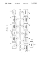
- FIG. 1 is a block diagram showing the overall construction of an embodiment of an image processing system according to the present invention.
- reference numeral 1 designates a control processor CPU for controlling the whole of the image processing system
- 2 a main memory for storing programs to be executed by the CPU 1, and for storing operation parameters which are used by the CPU 1
- 3 a disk device for storing programs, image data and document data.
- the disk device 3 includes several kinds of disk device used in accordance with the properties of data, for example, magnetic disk devices (including a hard disk device and a floppy disk device) and an optical disk device. Further, in FIG.
- reference numeral 4 designates a frame memory for writing therein information which is to be supplied to a CRT device 6, 5 a CRT controller for supplying the contents of the frame memory 4 to the CRT device 6, 7 a keyboard for inputting code data and commands for the CPU 1, 8 a facsimile device for sending image data to and receiving image data from an external system which is connected to the present image processing system through a communication line, 9 a scanner for supplying image data to the image memory 11, 10 an image processor which will be explained later in detail, 11 an image memory for temporarily storing image data, 12 a working memory, and 13 a printer for outputting image data and document data.
- FIG. 2 is a block diagram showing main functions of the present embodiment
- image data is given by, for example, the scanner 9 or the facsimile device 8, to be written in the image memory 11.
- the CPU 1 refers to or modifies the image data written in the image memory 11.
- the image data stored in the image memory 11 is subjected to image conversion by the image processor 10, outputting to the CRT 6 through the frame memory 4, outputting to the printer 13 or the facsimile device 8, or storing in the disk device 3 in accordance with a command from the CPU 1. Further, images stored in the disk device 3 are retrieved, to send a desired image to the image memory 11.
- FIGS. 3A and 3B are diagrams for explaining the fundamental construction and operation of an image processor.
- the image processor includes a local image extracting circuit 40 and a local image processing circuit 50.
- An example of the local image extracting circuit 40 includes cascade-connected shift registers 41 to 44.
- a local region S made up of 2 ⁇ 2 pixels which are adjacent to each other, can be extracted from the two-dimensional image (that is, original image) stored in the image memory 11.
- Original image data which is read out from the image memory 11 along each row of the original image is successively sent to the shift registers 41 and 42 through an input line 45.
- Each of the shift registers 41 and 42 can store therein image data of one pixel.
- the output of the shift register 42 is applied to the shift register 43 having a storage capacity of a plurality of pixels, and is then applied to the shift register 44 having a storage capacity of one pixel.
- the number of bits included in the shift register 43 is determined so that one row on the original image can be stored in the shift registers 43 and 44. Accordingly, when the input line 45 is supplied with, for example, the contents of the twenty-sixth pixel as shown in FIG. 3A, the shift registers 41, 42 and 44 and the rightmost bit of the shift register 43 can indicate the states of 2 ⁇ 2 pixels which are adjacent to each other on the original image, that is, the state of the local region S made up of four pixels.
- FIG. 3B shows the states of the shift registers 41 to 44 at a time the input line 45 receives the contents of the twenty-seventh pixel.
- a local region is extracted which is deviated from the local region of FIG. 3A by one pixel in the row direction.
- the local image extracting circuit 40 scans the original image with a window equal in size to 2 ⁇ 2 pixels, in synchronism with a reading operation for reading out image data from the image memory 11 bit by bit, and local images specified by the window are successively supplied to the local image processing circuit 50. It can be easily assumed that if an increased number m of shift registers are arranged in a row direction and increased number n of outputs are taken out from each shift register, local regions of an arbitrary size can be formed which include m ⁇ n pixels.
- FIG. 4A shows the fundamental structure and operation of an example of a high-speed image processor according to the present invention.
- a plurality of local image extracting circuits are operated in parallel, and the outputs of the local image extracting circuits are supplied to a plurality of local image processing circuits through a local image reconstruction circuit 49.
- two local image extracting circuits 40A and 40B are used, and the wiring pattern in the local image reconstruction circuit 49 is formed so that the output of shift registers 44A and 42A included in the first image extracting circuit 40A and the outputs of shift registers 44B and 42B included in the second local image extracting circuit 40B are supplied to a local image processing circuit 50A, and the outputs of shift registers 43A and 41A included in the first local image extracting circuit 40A and the outputs of the shift registers 44B and 42B included in the second local image extracting circuit 40B are supplied to another local image processing circuit 50B.
- FIG. 4A shows the states of the local regions S1 and S2 at a time the twenty-eighth and twenty-ninth pixels are read out
- FIG. 4B shows the states of the local regions S1 and S2 at a time the thirtieth and thirty-first pixels are read out.
- FIG. 5 shows another example of an image processor according to the present invention, which example includes three local image extracting circuits 40A, 40B and 40C connected in parallel, and shows a positional relation among three local regions S1, S2 and S3 extracted by this example. It is needless to say that an image processor according to the present invention can include a desired number of parallel-connected local image extracting circuits.
- FIG. 6 is a block diagram showing the circuit conjugation of the image processor 10 capable of processing local images in parallel.
- the image processor 10 is connected to the common bus 14 through a bus interface 20.
- the image processor 10 has an inner bus 21 connected to the bus interface 20, and further includes a direct memory access controller (DMAC) 30 on the input side, a DMAC 37 on the output side, and a control information register 61. Each of these members 30, 37 and 61 is connected to the inner bus 21.
- the DMAC 30 fetches image data stored in the image memory 11, into a buffer memory 31 without receiving the aid of the CPU 1.
- a starting address SA for indicating that location in the image memory where the head of a data area to be read out is stored, a line length L1 for indicating the length of the data area in a transverse direction, and the number N1 of lines for indicating the length of the data area in the longitudinal direction are previously specified by the CPU 1, and stored in registers 30A, 30B and 30C, respectively.
- the DMAC 37 includes registers 37A to 37C, to indicate that area of the image memory where image data having been subjected to image processing is to be written.
- a destination address DA for indicating that location in the image memory where the head of the image data is written, a line length L2, and the number N2 of lines, are written in the register 37A, 37B and 37C, respectively.
- the parameters DA, L2 and N2 are specified by the CPU 1.
- Original image data stored in the buffer memory 31 is supplied to a parallel-series converter 32 in a block of l bits, and is outputted from the converter 32 bit by bit.
- the local image extracting circuits 40A and 40B alternately receive the image data from the converter 32.
- the pixel data which is delivered from the local image extracting circuits, is rearranged by the local image reconstruction circuit 49.
- Image data from the reconstruction circuit 49 is supplied to the local image processing circuits 50A and 50B in parallel.
- Pixel data which has completed a predetermined image processing by the local image processing circuits 50A and 50B is supplied to a serial-parallel converter 35 in order to convert it into parallel data.
- the parallel data is temporarily stored in a buffer memory 36, and then written in a predetermined area of the image memory 11 with the aid of the DMAC 37.
- Reference numeral 62 in FIG. 6 designates an input control circuit for controlling the data transfer in an input portion made up of the DMAC 30, the buffer memory 31, the parallel-series converter 32 and the local image extracting circuits 40A and 40B. Further, reference numeral 63 designates an output control circuit for controlling the data transfer in an output portion made up of the local image processing circuits 50A and 50B, the series-parallel converter 35, the buffer memory 36 and the DMAC 37. These control circuits 62 and 63 operate according to control parameters which are set in a control information register 61 by the CPU 1.
- Each of the local image processing circuits 50A and 50B performs a predetermined, discriminating or recognition operation for respective successively-supplied local images, each made up of a plurality of pixels, and delivers one modified pixel to every local image.
- the contents of a processing which is carried out by each local image processing circuit, are specified by a parameter control circuit 64.
- FIG. 7 shows the circuit configuration of the input and output portions of the image processor 10 in more detail.
- image data is read out from the image memory 11 in a block of 32 bits, with the aid of the DMAC 30.
- the read-out image data is sent to buffer memories 31A and 31B through a data line 100 and a multiplexer (MPX) 71, to be stored in the buffer memories 31A and 31B in a predetermined order.
- MPX multiplexer
- a flip-flop circuit 72 controls the switch over of one output of the MPX 71 to the other output, and the state of the flip-flop circuit 72 is specified by a control signal 101 from the DMAC 30.
- the outputs of the buffer memories 31A and 31B are supplied to a selector 32.
- the selector 32 takes in the output of one of the buffer memories 31A and 31B in accordance with a counter value 102 which is indicated by a counter circuit 73 for counting clock pulses CL from a clock generator 70.
- Input data to the selector 32 is converted by the selector 32 into serial pixel data and is alternately supplied to the local image extracting circuits 40A and 40B.
- the operation of the counter circuit 73 is controlled by a reset signal 103 and an enable signal 104 each supplied from the input control circuit 62.
- the counter circuit 73 counts clock pulses circularly up to an upper limit value which is equal to the number of pixels included in one row of image data, for example, up to 31.
- FIG. 8 shows an example of a relation among the counter value 102 of the counter Circuit 73, a buffer memory selected by the selector 32, and pixels inputted to the local image extracting circuits 40A and 40B.
- the buffer memory 31A is selected for a period when the counter value lies in a range from 0 to 15. In this period, the local image extracting circuits 40A and 40B alternately receive one pixel data each time the counter value 102 is updated. Further, the buffer memory 31B is selected for a period when the counter value lies in a range from 16 to 31.
- the local image extracting circuits 40A and 40B alternately receive one pixel data each time the counter value is updated.
- the DMAC 30 changes the state of the flip-flop circuit 72 in accordance with the counter value 102 so that after 32-bit data has been written in one of the buffer memories 31A and 31B, the next 32-bit data is written in the other buffer memory.
- original image data stored in the image memory 11 can be successively supplied to the buffer memories 31A and 31B.
- image data processed by the local image processing circuits 50A and 50B are temporarily stored in a multiplexer 35, to be sent to a buffer memory 36A in a block of 32 bits.
- the multiplexer 35 takes in pixel data from the local image processing circuits 50A and 50B in response to the update of a counter value 107 which is indicated by a counter circuit 81 for counting up the clock pulses CL, and converts the input data into a block of parallel data composed of 32 bits.
- the operation of the counter circuit 81 is controlled by a reset signal 105 and an enable signal 106 which are supplied from the output control circuit 63.
- Image data stored in the buffer memory 36A is transferred to another buffer memory 36B, and then written in the image memory 11 with the aid of the DMAC 37.
- the image processor of FIG. 7 includes two local image extracting circuits 40A and 40B and two local image processing circuits 50A and 50B, to process two local images in parallel.
- the image processor of FIG. 7 includes two local image extracting circuits 40A and 40B and two local image processing circuits 50A and 50B, to process two local images in parallel.
- the speed of image processing can be greatly increased
- FIG. 10 shows an embodiment of a local image processing circuit 50 according to the present invention.
- the image processor of FIG. 7 two local image processing circuits are used for two local image extracting circuits.
- the states of m ⁇ n pixels of the local image S1 from the reconstruction circuit 49 are applied, as a select signal, to a selector 53A, and the states of m ⁇ n pixels of the local image S2 are applied, as a select signal, to another selector 53B.
- Image processing is to determine the state of an output pixel in accordance with the state of an input local image, that is, the combination of the states of m ⁇ n pixels included in the local image.
- processing results that is, values of output pixel
- C 1 to C n corresponding to various combinations of the states of m ⁇ n pixels are previously written in a memory 52, and the values C l to C n are applied to each of the selectors 53A and 53B. That one of the values C l to C n which is specified by an address corresponding to the combination of the states of m ⁇ n pixels of the local image S1, is selected by the selector 53A, to be delivered therefrom as modified pixel data Pa (namely, pixel data after image processing).
Landscapes
- Engineering & Computer Science (AREA)
- Physics & Mathematics (AREA)
- General Physics & Mathematics (AREA)
- Theoretical Computer Science (AREA)
- Multimedia (AREA)
- Image Processing (AREA)
Applications Claiming Priority (2)
| Application Number | Priority Date | Filing Date | Title |
|---|---|---|---|
| JP1049826A JPH02230383A (ja) | 1989-03-03 | 1989-03-03 | 画像処理装置 |
| JP1-49826 | 1989-03-03 |
Publications (1)
| Publication Number | Publication Date |
|---|---|
| US5117468A true US5117468A (en) | 1992-05-26 |
Family
ID=12841903
Family Applications (1)
| Application Number | Title | Priority Date | Filing Date |
|---|---|---|---|
| US07/486,436 Expired - Lifetime US5117468A (en) | 1989-03-03 | 1990-02-28 | Image processing system capable of carrying out local processing for image at high speed |
Country Status (3)
| Country | Link |
|---|---|
| US (1) | US5117468A (ja) |
| JP (1) | JPH02230383A (ja) |
| KR (1) | KR930003413B1 (ja) |
Cited By (11)
| Publication number | Priority date | Publication date | Assignee | Title |
|---|---|---|---|---|
| US5565882A (en) * | 1991-03-26 | 1996-10-15 | Victor Company Of Japan, Ltd. | Image processing system for display, recording and reproducing image |
| US5655131A (en) * | 1992-12-18 | 1997-08-05 | Xerox Corporation | SIMD architecture for connection to host processor's bus |
| US5790708A (en) * | 1993-03-25 | 1998-08-04 | Live Picture, Inc. | Procedure for image processing in a computerized system |
| US5794016A (en) * | 1995-12-11 | 1998-08-11 | Dynamic Pictures, Inc. | Parallel-processor graphics architecture |
| US6151412A (en) * | 1990-09-12 | 2000-11-21 | Canon Kabushiki Kaisha | Image processing apparatus having capability of synthesizing contents of plural memories |
| US6219466B1 (en) * | 1998-10-05 | 2001-04-17 | Nec Corporation | Apparatus for implementing pixel data propagation using a linear processor array |
| US20010022864A1 (en) * | 2000-02-29 | 2001-09-20 | Taiji Iwasaki | Image processing apparatus and image processing program storage medium |
| US6351261B1 (en) | 1993-08-31 | 2002-02-26 | Sun Microsystems, Inc. | System and method for a virtual reality system having a frame buffer that stores a plurality of view points that can be selected and viewed by the user |
| US6940496B1 (en) * | 1998-06-04 | 2005-09-06 | Silicon, Image, Inc. | Display module driving system and digital to analog converter for driving display |
| US7254283B1 (en) * | 1998-11-13 | 2007-08-07 | Minolta Co., Ltd. | Image processor processing image data in parallel with a plurality of processors |
| US10026140B2 (en) | 2005-06-10 | 2018-07-17 | Nvidia Corporation | Using a scalable graphics system to enable a general-purpose multi-user computer system |
Families Citing this family (1)
| Publication number | Priority date | Publication date | Assignee | Title |
|---|---|---|---|---|
| JP6414388B2 (ja) * | 2014-04-18 | 2018-10-31 | 株式会社リコー | アクセラレータ回路及び画像処理装置 |
Citations (4)
| Publication number | Priority date | Publication date | Assignee | Title |
|---|---|---|---|---|
| US4363104A (en) * | 1980-09-22 | 1982-12-07 | Hughes Aircraft Company | Imaging system having multiple image copying and hierarchical busing |
| US4484349A (en) * | 1982-03-11 | 1984-11-20 | Environmental Research Institute Of Michigan | Parallel pipeline image processor |
| US4550437A (en) * | 1981-06-19 | 1985-10-29 | Hitachi, Ltd. | Apparatus for parallel processing of local image data |
| US4710965A (en) * | 1984-07-30 | 1987-12-01 | Ricoh Company, Ltd. | Image data masking device |
-
1989
- 1989-03-03 JP JP1049826A patent/JPH02230383A/ja active Pending
-
1990
- 1990-02-15 KR KR1019900001836A patent/KR930003413B1/ko not_active Expired - Fee Related
- 1990-02-28 US US07/486,436 patent/US5117468A/en not_active Expired - Lifetime
Patent Citations (4)
| Publication number | Priority date | Publication date | Assignee | Title |
|---|---|---|---|---|
| US4363104A (en) * | 1980-09-22 | 1982-12-07 | Hughes Aircraft Company | Imaging system having multiple image copying and hierarchical busing |
| US4550437A (en) * | 1981-06-19 | 1985-10-29 | Hitachi, Ltd. | Apparatus for parallel processing of local image data |
| US4484349A (en) * | 1982-03-11 | 1984-11-20 | Environmental Research Institute Of Michigan | Parallel pipeline image processor |
| US4710965A (en) * | 1984-07-30 | 1987-12-01 | Ricoh Company, Ltd. | Image data masking device |
Cited By (16)
| Publication number | Priority date | Publication date | Assignee | Title |
|---|---|---|---|---|
| US6151412A (en) * | 1990-09-12 | 2000-11-21 | Canon Kabushiki Kaisha | Image processing apparatus having capability of synthesizing contents of plural memories |
| US5565882A (en) * | 1991-03-26 | 1996-10-15 | Victor Company Of Japan, Ltd. | Image processing system for display, recording and reproducing image |
| US5655131A (en) * | 1992-12-18 | 1997-08-05 | Xerox Corporation | SIMD architecture for connection to host processor's bus |
| US6763146B2 (en) | 1993-03-25 | 2004-07-13 | Roxio, Inc. | Method and system for image processing |
| US5790708A (en) * | 1993-03-25 | 1998-08-04 | Live Picture, Inc. | Procedure for image processing in a computerized system |
| US5907640A (en) * | 1993-03-25 | 1999-05-25 | Live Picture, Inc. | Functional interpolating transformation system for image processing |
| US6181836B1 (en) | 1993-03-25 | 2001-01-30 | Mgi Software Corporation | Method and system for non-destructive image editing |
| USRE43747E1 (en) | 1993-03-25 | 2012-10-16 | Intellectual Ventures I Llc | Method and system for image processing |
| US6512855B1 (en) | 1993-03-25 | 2003-01-28 | Roxio, Inc. | Method and system for image processing |
| US6351261B1 (en) | 1993-08-31 | 2002-02-26 | Sun Microsystems, Inc. | System and method for a virtual reality system having a frame buffer that stores a plurality of view points that can be selected and viewed by the user |
| US5794016A (en) * | 1995-12-11 | 1998-08-11 | Dynamic Pictures, Inc. | Parallel-processor graphics architecture |
| US6940496B1 (en) * | 1998-06-04 | 2005-09-06 | Silicon, Image, Inc. | Display module driving system and digital to analog converter for driving display |
| US6219466B1 (en) * | 1998-10-05 | 2001-04-17 | Nec Corporation | Apparatus for implementing pixel data propagation using a linear processor array |
| US7254283B1 (en) * | 1998-11-13 | 2007-08-07 | Minolta Co., Ltd. | Image processor processing image data in parallel with a plurality of processors |
| US20010022864A1 (en) * | 2000-02-29 | 2001-09-20 | Taiji Iwasaki | Image processing apparatus and image processing program storage medium |
| US10026140B2 (en) | 2005-06-10 | 2018-07-17 | Nvidia Corporation | Using a scalable graphics system to enable a general-purpose multi-user computer system |
Also Published As
| Publication number | Publication date |
|---|---|
| KR930003413B1 (ko) | 1993-04-29 |
| KR900015030A (ko) | 1990-10-25 |
| JPH02230383A (ja) | 1990-09-12 |
Similar Documents
| Publication | Publication Date | Title |
|---|---|---|
| EP0012173B1 (en) | Apparatus for picture processing with resolution conversion | |
| EP0216501B1 (en) | Digital image rotation | |
| US5117468A (en) | Image processing system capable of carrying out local processing for image at high speed | |
| HK1002718A1 (en) | Device for displaying a composite image | |
| JPS5850589A (ja) | 表示処理装置 | |
| CN1253335A (zh) | 在计算机显示器上的图象的硬件旋转 | |
| JPS6330632B2 (ja) | ||
| US6031546A (en) | Image processing apparatus and method | |
| US4647971A (en) | Moving video special effects system | |
| US6606673B2 (en) | Direct memory access transfer apparatus | |
| US4809343A (en) | Maximum/minimum value conversion circuit for image processing | |
| JPS613193A (ja) | 画像メモリの書込み/読出し変換方式 | |
| EP0145530A2 (en) | Arrangement for providing data signals for a data display system | |
| JPH028335B2 (ja) | ||
| JPH11306343A (ja) | 2次元データ回転処理装置 | |
| US6195463B1 (en) | Multiresolution image processing and storage on a single chip | |
| KR950008023B1 (ko) | 래스터 주사 표시 시스템 | |
| JPH07107706B2 (ja) | 遅延段数の可変なラインバツフア | |
| US5721884A (en) | Apparatus for combining and separating color component data in an image processing system | |
| JPH0752468B2 (ja) | 線画表示用マルチプロセツサ | |
| JPH05113928A (ja) | 画像メモリ装置 | |
| JPH07264395A (ja) | 画像縮小装置 | |
| JPH09212637A (ja) | 画像処理プロセッサ | |
| EP0242139A2 (en) | Display controller | |
| JP2647380B2 (ja) | カラー画像処理装置 |
Legal Events
| Date | Code | Title | Description |
|---|---|---|---|
| AS | Assignment |
Owner name: HITACHI, LTD., JAPAN Free format text: ASSIGNMENT OF ASSIGNORS INTEREST.;ASSIGNORS:HINO, MASATOSHI;FUKUDA, KOUJI;MACHIDA, TETSUO;REEL/FRAME:005248/0505 Effective date: 19900223 |
|
| STCF | Information on status: patent grant |
Free format text: PATENTED CASE |
|
| FEPP | Fee payment procedure |
Free format text: PAYOR NUMBER ASSIGNED (ORIGINAL EVENT CODE: ASPN); ENTITY STATUS OF PATENT OWNER: LARGE ENTITY |
|
| FPAY | Fee payment |
Year of fee payment: 4 |
|
| FPAY | Fee payment |
Year of fee payment: 8 |
|
| FPAY | Fee payment |
Year of fee payment: 12 |